ICGOO在线商城 > 集成电路(IC) > PMIC - 稳压器 - 线性 > LT1085IM#PBF
/LT1085IM#PBF.jpg)
 Datasheet下载
- 型号: LT1085IM#PBF
- 制造商: LINEAR TECHNOLOGY
- 库位|库存: xxxx|xxxx
- 要求:
| 数量阶梯 | 香港交货 | 国内含税 |
| +xxxx | $xxxx | ¥xxxx |
查看当月历史价格
查看今年历史价格
LT1085IM#PBF产品简介:
ICGOO电子元器件商城为您提供LT1085IM#PBF由LINEAR TECHNOLOGY设计生产,在icgoo商城现货销售,并且可以通过原厂、代理商等渠道进行代购。 LT1085IM#PBF价格参考。LINEAR TECHNOLOGYLT1085IM#PBF封装/规格:PMIC - 稳压器 - 线性, Linear Voltage Regulator IC Positive Adjustable 1 Output 1.25 V ~ 28.5 V 3A D2PAK-3。您可以下载LT1085IM#PBF参考资料、Datasheet数据手册功能说明书,资料中有LT1085IM#PBF 详细功能的应用电路图电压和使用方法及教程。
LT1085IM#PBF 是由 Linear Technology(现为 Analog Devices)生产的一款线性稳压器,属于 PMIC(电源管理集成电路)类别。它具有低噪声、高精度和良好的热性能等特点,适用于多种电子设备中的电源管理场景。以下是其主要应用场景:

 1. 工业设备
   - 传感器供电:为工业传感器提供稳定电压,确保测量数据的准确性和可靠性。
   - 嵌入式系统:用于工业控制板或嵌入式系统的电源管理,提供稳定的低压输出。
   - 仪器仪表:为精密仪器提供低噪声电源,保证测量精度。

 2. 通信设备
   - 信号处理模块:为通信设备中的信号处理芯片供电,确保信号质量。
   - 基站辅助电源:作为基站中低功耗模块的备用电源或辅助电源。

 3. 医疗设备
   - 便携式医疗设备:如血压计、血糖仪等,提供低功耗、稳定的电源。
   - 监护设备:为心率监测仪、血氧仪等设备提供低噪声电源,减少对信号采集的干扰。

 4. 消费类电子产品
   - 音频设备:为耳机放大器、音响等提供低噪声电源,提升音质表现。
   - 便携式设备:如电子阅读器、手持游戏机等,提供高效、稳定的电源支持。

 5. 汽车电子
   - 车载信息娱乐系统:为导航、音响等系统提供稳定的电源。
   - 传感器模块:为汽车中的温度、压力等传感器提供电源支持。

 6. 其他应用
   - 电池供电设备:在电池驱动的设备中,作为降压稳压器,延长电池寿命。
   - 实验与开发:在实验室环境中,用于测试和验证电路设计。

 特点总结
LT1085IM#PBF 的典型应用场景包括需要低噪声、高精度电压输出的场合,特别适合对电源稳定性要求较高的设备。其封装形式和电气特性使其能够适应各种复杂的工作环境,是一款广泛应用于工业、医疗、通信和消费领域的高性能线性稳压器。
| 参数 | 数值 |
| 产品目录 | 集成电路 (IC) |
| 描述 | IC REG LDO ADJ 3A D2PAK |
| 产品分类 | |
| 品牌 | Linear Technology |
| 数据手册 | http://www.linear.com/docs/3741 |
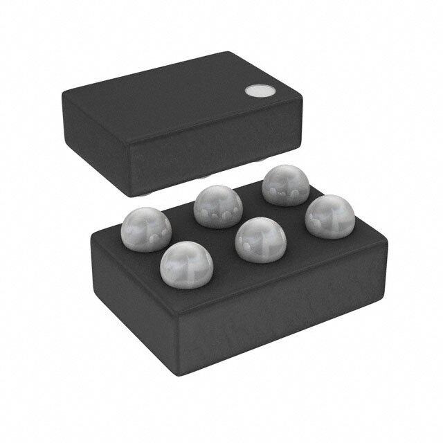
| 产品图片 |
|
| 产品型号 | LT1085IM#PBF |
| rohs | 无铅 / 符合限制有害物质指令(RoHS)规范要求 |
| 产品系列 | - |
| 产品培训模块 | http://www.digikey.cn/PTM/IndividualPTM.page?site=cn&lang=zhs&ptm=30565 |
| 供应商器件封装 | D2PAK-3 |
| 其它名称 | LT1085IMPBF |
| 包装 | 管件 |
| 安装类型 | 表面贴装 |
| 封装/外壳 | TO-263-4,D²Pak(3 引线+接片),TO-263AA |
| 工作温度 | -40°C ~ 125°C |
| 标准包装 | 50 |
| 电压-跌落(典型值) | 1.3V @ 3A |
| 电压-输入 | 2.55 V ~ 30 V |
| 电压-输出 | 1.25 V ~ 28.5 V |
| 电流-输出 | 3A |
| 电流-限制(最小值) | 3.2A |
| 稳压器拓扑 | 正,可调式 |
| 稳压器数 | 1 |


- 商务部:美国ITC正式对集成电路等产品启动337调查
- 曝三星4nm工艺存在良率问题 高通将骁龙8 Gen1或转产台积电
- 太阳诱电将投资9.5亿元在常州建新厂生产MLCC 预计2023年完工
- 英特尔发布欧洲新工厂建设计划 深化IDM 2.0 战略
- 台积电先进制程称霸业界 有大客户加持明年业绩稳了
- 达到5530亿美元!SIA预计今年全球半导体销售额将创下新高
- 英特尔拟将自动驾驶子公司Mobileye上市 估值或超500亿美元
- 三星加码芯片和SET,合并消费电子和移动部门,撤换高东真等 CEO
- 三星电子宣布重大人事变动 还合并消费电子和移动部门
- 海关总署:前11个月进口集成电路产品价值2.52万亿元 增长14.8%


PDF Datasheet 数据手册内容提取
LT1083/LT1084/LT1085 7.5A, 5A, 3A Low Dropout Positive Adjustable Regulators FeaTures DescripTion n 3-Terminal Adjustable The LT®1083 series of positive adjustable regulators are n Output Current of 3A, 5A or 7.5A designed to provide 7.5A, 5A and 3A with higher efficiency n Operates Down to 1V Dropout than currently available devices. All internal circuitry is n Guaranteed Dropout Voltage at Multiple Current Levels designed to operate down to 1V input-to-output differential n Line Regulation: 0.015% and the dropout voltage is fully specified as a function of n Load Regulation: 0.1% load current. Dropout is guaranteed at a maximum of 1.5V n 100% Thermal Limit Functional Test at maximum output current, decreasing at lower load cur- n Fixed Versions Available rents. On-chip trimming adjusts the reference voltage to n Available in 3-Lead Plastic TO-220 and DD Packages 1%. Current limit is also trimmed, minimizing the stress on both the regulator and power source circuitry under overload conditions. applicaTions The LT1083/LT1084/LT1085 devices are pin compatible n High Efficiency Linear Regulators with older 3-terminal regulators. A 10µF output capacitor n Post Regulators for Switching Supplies is required on these new devices. However, this is included n Constant Current Regulators in most regulator designs. n Battery Chargers Unlike PNP regulators, where up to 10% of the output cur- DEVICE OUTPUT CURRENT* rent is wasted as quiescent current, the LT1083 quiescent LT1083 7.5A current flows into the load, increasing efficiency. LT1084 5.0A LT1085 3.0A L, LT, LTC, LTM, Linear Technology and the Linear logo are registered trademarks and UltraFast and ThinSOT are trademarks of Linear Technology Corporation. All other trademarks *For a 1.5A low dropout regulator see the LT1086 data sheet. are the property of their respective owners. Typical applicaTion Dropout Voltage vs Output Current 2 5V, 7.5A Regulator V) L ( A TI N E R VIN ≥ 6.5V IN LT1083 OUT 5V AT 7.5A FE F + ADJ 112%1Ω + AGE DI 1 10µF 10µF* LT TANTALUM VO 365Ω UT 1% TP U *REQUIRED FOR STABILITY O 1083/4/5 ADJ TA01 T/ U P N I 0 0 IFULL LOAD OUTPUT CURRENT 1083/4/5 ADJ TA02 108345fh 1 For more information www.linear.com/LT1083
LT1083/LT1084/LT1085 absoluTe MaxiMuM raTings (Note 1) Power Dissipation ...............................Internally Limited M-Grades: (OBSOLETE) Input-to-Output Voltage Differential Control Section ...............–55°C to 150°C C-Grades ...............................................................30V Power Transistor .............–55°C to 200°C I-Grades ................................................................30V Storage Temperature Range ..................–65°C to 150°C M-Grades (OBSOLETE) ........................................35V Lead Temperature (Soldering, 10 sec) ...................300°C Operating Junction Temperature Range (Note 9) preconDiTioning C-Grades: Control Section ...................0°C to 125°C Power Transistor .................0°C to 150°C 100% thermal shutdown functional test. I-Grades: Control Section ...............–40°C to 125°C Power Transistor .............–40°C to 150°C pin conFiguraTion TAB IS FRONT VIEW FRONT VIEW OUTPUT TAB 3 VIN 3 VIN IS 2 VOUT 2 VOUT OUTPUT 1 ADJ 1 ADJ P PACKAGE T PACKAGE 3-LEAD PLASTIC TO-220 3-LEAD PLASTIC TO-3P θJA = 35°C/W θJA = 50°C/W OBSOLETE PACKAGE BOTTOM VIEW FRONT VIEW VIN CASE IS OUTPUT 33 VIN 2 TAB IS 22 VOUT OUTPUT 1 11 ADJ ADJ M PACKAGE 3-LEAD PLASTIC DD K PACKAGE 2-LEAD TO-3 METAL CAN θJA = 30°C/W* *WITH PACKAGE SOLDERED TO 0.5IN2 COPPER AREA OVER θJA = 35°C/W BACKSIDE GROUND PLANE OR INTERNAL POWER PLANE. θJA CAN VARY OBSOLETE PACKAGE FROM 20°C/W TO >40°C/W DEPENDING ON MOUNTING TECHNIQUE 108345fh 2 For more information www.linear.com/LT1083
LT1083/LT1084/LT1085 orDer inForMaTion LEAD FREE FINISH TAPE AND REEL PART MARKING PACKAGE DESCRIPTION TEMPERATURE RANGE LT1083CP#PBF NA LT1083CP 3-Lead Plastic TO-3P Control: 0°C to 125°C Power: 0°C to 150°C LT1084CP#PBF NA LT1084CP 3-Lead Plastic TO-3P Control: 0°C to 125°C Power: 0°C to 150°C OBSOLETE PACKAGE LT1084CT#PBF NA LT1084CT 3-Lead Plastic TO-220 Control: 0°C to 125°C Power: 0°C to 150°C LT1084IT#PBF NA LT1084IT 3-Lead Plastic TO-220 Control: –40°C to 125°C Power: –40°C to 150°C LT1085CT#PBF NA LT1085CT 3-Lead Plastic TO-220 Control: 0°C to 125°C Power: 0°C to 150°C LT1085IT#PBF NA LT1085IT 3-Lead Plastic TO-220 Control: –40°C to 125°C Power: –40°C to 150°C LT1085CM#PBF LT1085CM#TRPBF LT1085CM 3-Lead Plastic DD Control: 0°C to 125°C Power: 0°C to 150°C LT1085IM#PBF LT1085IM#TRPBF LT1085IM 3-Lead Plastic DD Control: –40°C to 125°C Power: –40°C to 150°C LEAD BASED FINISH TAPE AND REEL PART MARKING PACKAGE DESCRIPTION TEMPERATURE RANGE LT1083CP NA LT1083CP 3-Lead Plastic TO-3P Control: 0°C to 125°C Power: 0°C to 150°C LT1084CP NA LT1084CP 3-Lead Plastic TO-3P Control: 0°C to 125°C Power: 0°C to 150°C OBSOLETE PACKAGE LT1084CT NA LT1084CT 3-Lead Plastic TO-220 Control: 0°C to 125°C Power: 0°C to 150°C LT1084IT NA LT1084IT 3-Lead Plastic TO-220 Control: –40°C to 125°C Power: –40°C to 150°C LT1085CT NA LT1085CT 3-Lead Plastic TO-220 Control: 0°C to 125°C Power: 0°C to 150°C LT1085IT NA LT1085IT 3-Lead Plastic TO-220 Control: –40°C to 125°C Power: –40°C to 150°C LT1085CM LT1085CM#TR LT1085CM 3-Lead Plastic DD Control: 0°C to 125°C Power: 0°C to 150°C LT1085IM LT1085IM#TR LT1085IM 3-Lead Plastic DD Control: –40°C to 125°C Power: –40°C to 150°C 108345fh 3 For more information www.linear.com/LT1083
LT1083/LT1084/LT1085 orDer inForMaTion LEAD BASED FINISH TAPE AND REEL PART MARKING PACKAGE DESCRIPTION TEMPERATURE RANGE LT1083CK NA LT1083CK 2-Lead TO-3 Metal Can Control: 0°C to 125°C Power: 0°C to 150°C LT1083MK NA LT1083MK 2-Lead TO-3 Metal Can Control: –55°C to 150°C Power: –55°C to 200°C LT1084CK NA LT1084CK 2-Lead TO-3 Metal Can Control: 0°C to 125°C Power: 0°C to 150°C LT1084MK NA LT1084MK 2-Lead TO-3 Metal Can Control: –55°C to 150°C Power: –55°C to 200°C LT1085CK NA LT1085CK 2-Lead TO-3 Metal Can Control: 0°C to 125°C Power: 0°C to 150°C LT1085MK NA LT1085MK 2-Lead TO-3 Metal Can Control: –55°C to 150°C Power: –55°C to 200°C OBSOLETE PACKAGE Consult LTC Marketing for parts specified with wider operating temperature ranges. For more information on lead free part marking, go to: http://www.linear.com/leadfree/ For more information on tape and reel specifications, go to: http://www.linear.com/tapeandreel/ 108345fh 4 For more information www.linear.com/LT1083
LT1083/LT1084/LT1085 elecTrical characTerisTics The l denotes the specifications which apply over the full operating temperature range, otherwise specifications are at T = 25°C. A PARAMETER CONDITIONS MIN TYP MAX UNITS Reference Voltage I = 10mA, T = 25°C, OUT J (V – V ) = 3V 1.238 1.250 1.262 V IN OUT 10mA ≤ I ≤ I OUT FULL_LOAD l 1.5V ≤ (V –V ) ≤ 25V (Notes 4, 6, 7) 1.225 1.250 1.270 V IN OUT Line Regulation I = 10mA, 1.5V ≤ (V – V ) ≤ 15V, T = 25°C (Notes 2, 3) 0.015 0.2 % LOAD IN OUT J l 0.035 0.2 % M-Grade: 15V ≤ (V –V ) ≤ 35V (Notes 2, 3) l 0.05 0.5 % IN OUT C-, I-Grades: 15V ≤ (V –V ) ≤ 30V (Notes 2, 3) l 0.05 0.5 % IN OUT Load Regulation (V – V ) = 3V, 10mA ≤ I ≤ I ,T = 25°C 0.1 0.3 % IN OUT OUT FULL_LOAD J (Notes 2, 3, 4, 6) l 0.2 0.4 % Dropout Voltage ∆V = 1%, I = I (Notes 5, 6, 8) l 1.3 1.5 V REF OUT FULL_LOAD Current Limit LT1083 (V – V ) = 5V l 8.0 9.5 A IN OUT l (V – V ) = 25V 0.4 1.0 A IN OUT l LT1084 (V – V ) = 5V 5.5 6.5 A IN OUT l (V – V ) = 25V 0.3 0.6 A IN OUT l LT1085 (V – V ) = 5V 3.2 4.0 A IN OUT l (V – V ) = 25V 0.2 0.5 A IN OUT Minimum Load Current (V – V ) = 25V l 5 10 mA IN OUT Thermal Regulation T = 25°C, 30ms Pulse A LT1083 0.002 0.010 %/W LT1084 0.003 0.015 %/W LT1085 0.004 0.020 %/W Ripple Rejection f = 120Hz, C = 25µF, C = 25µF Tantalum l 60 75 dB ADJ OUT I = I , (V – V ) = 3V (Notes 6, 7, 8) OUT FULL_LOAD IN OUT Adjust Pin Current T = 25°C 55 µA J l 120 µA Adjust Pin Current Change 10mA ≤ I ≤ I ,1.5V ≤ (V – V ) ≤ 25V (Note 6) l 0.2 5 µA OUT FULL_LOAD IN OUT Temperature Stability l 0.5 % Long-Term Stability T = 125°C, 1000 Hrs 0.3 1 % A RMS Output Noise (% of V ) T = 25°C, 10Hz = ≤ f ≤ 10kHz 0.003 % OUT A Thermal Resistance Junction-to-Case Control Circuitry/Power Transistor LT1083 K Package 0.6/1.6 °C/W P Package 0.5/1.6 °C/W LT1084 K Package 0.75/2.3 °C/W P Package 0.65/2.3 °C/W T Package 0.65/2.7 °C/W LT1085 K Package 0.9/3.0 °C/W M, T Package 0.7/3.0 °C/W 108345fh 5 For more information www.linear.com/LT1083
LT1083/LT1084/LT1085 elecTrical characTerisTics Note 1: Stresses beyond those listed under Absolute Maximum Ratings Note 4: I is defined in the current limit curves. The I FULL_LOAD FULL_LOAD may cause permanent damage to the device. Exposure to any Absolute curve is defined as the minimum value of current limit as a function of Maximum Rating condition for extended periods may affect device input-to-output voltage. Note that the 60W power dissipation for the reliability and lifetime. LT1083 (45W for the LT1084 (K, P), 30W for the LT1084 (T), 30W for the Note 2: See thermal regulation specifications for changes in output voltage LT1085) is only achievable over a limited range of input-to-output voltage. due to heating effects. Load and line regulation are measured at a constant Note 5: Dropout voltage is specified over the full output current range of junction temperature by low duty cycle pulse testing. the device. Test points and limits are shown on the Dropout Voltage curve. Note 3: Line and load regulation are guaranteed up to the maximum power Note 6: For LT1083 I is 5A for –55°C ≤ T < –40°C and 7.5A for FULL_LOAD J dissipation (60W for the LT1083, 45W for the LT1084 (K, P), 30W for the T ≥ –40°C. J LT1084 (T) and 30W for the LT1085). Power dissipation is determined by Note 7: 1.7V ≤ (V – V ) ≤ 25V for LT1084 at –55°C ≤ T ≤ –40°C. IN OUT J the input/output differential and the output current. Guaranteed maximum Note 8: Dropout is 1.7V maximum for LT1084 at –55°C ≤ T ≤ –40°C. J power dissipation will not be available over the full input/output voltage Note 9: The LT1083/LT1084/LT1085 regulators are tested and specified range. under pulse load conditions such that TJ ≅ TA. The C-grade LT1083/ LT1084/LT1085 are 100% tested at 25°C.The I-grade LT1084/LT1085 are guaranteed over the full –40°C to 125°C operating ambient temperature range. 108345fh 6 For more information www.linear.com/LT1083
LT1083/LT1084/LT1085 Typical perForMance characTerisTics LT1083 LT1083 LT1083 Dropout Voltage Short-Circuit Current Load Regulation 2 12 0.10 L (V) INDICATES GUARANTEED TEST POINT ∆I = 7.5A DIFFERENTIA 0°C ≤ TJ –≤4 102°5C° ≤C TJ ≤ 150°C RRENT (A) 108 251°5C0°C VIATION (%) 0.005 NIMUM INPUT/OUTPUT 1 TJ = –T5J5 °=C 2T5J °=C 150°C SHORT-CIRCUIT CU 462 –5IF5U°LCL LOAD OUTPUT VOLTAGE DE–––000...011550 MI GUARANTEED 0 0 –0.20 0 1 2 3 4 5 6 7 8 9 10 0 5 10 15 20 25 30 35 –50 –25 0 25 50 75 100 125 150 OUTPUT CURRENT (A) INPUT/OUTPUT DIFFERENTIAL (V) TEMPERATURE (°C) LT1083/4/5 ADJ G01 LT1083/4/5 ADJ G02 LT1083/4/5 ADJ G03 LT1084 LT1084 LT1084 Dropout Voltage Short-Circuit Current Load Regulation 2 10 0.10 V) INDICATES GUARANTEED TEST POINT L ( 9 ∆I = 5A T/OUTPUT DIFFERENTIA 1 0°C ≤ TJ ≤ 12–55°5C°C ≤ TJ ≤ 15T0J° =C –55°C CIRCUIT CURRENT (A) 64578 150°C 25–°5C5°C OLTAGE DEVIATION (%)–00..00550 MINIMUN INPU TJ = 150°C TJ = 25°C SHORT- 321 GUAIFRUALNL TLEOEADD OUTPUT V––00..1150 0 0 –0.20 0 1 2 3 4 5 6 0 5 10 15 20 25 30 35 –50 –25 0 25 50 75 100 125 150 OUTPUT CURRENT (A) INPUT/OUTPUT DIFFERENTIAL (V) TEMPERATURE (°C) LT1083/4/5 ADJ G04 LT1083/4/5 ADJ G05 LT1083/4/5 ADJ G06 LT1085 LT1085 LT1085 Dropout Voltage Short-Circuit Current Load Regulation 2 6 0.10 V) INDICATES GUARANTEED TEST POINT L ( ∆I = 3A DIFFERENTIA 0°C ≤ TJ ≤ 1–2555°°CC ≤ TJ ≤ 150°C RRENT (A) 54 25°C VIATION (%) 0.005 MUM INPUT/OUTPUT 1 TJ = 150°C TJ = 25°C TJ = –55°C SHORT-CIRCUIT CU 231 GU–AI5FR5UA°LCNL TLEOEADD 150°C OUTPUT VOLTAGE DE –––000...110505 NI MI 0 0 –0.20 0 1 2 3 4 0 5 10 15 20 25 30 35 –50 –25 0 25 50 75 100 125 150 OUTPUT CURRENT (A) INPUT/OUTPUT DIFFERENTIAL (V) TEMPERATURE (°C) LT1083/4/5 ADJ G07 LT1083/4/5 ADJ G08 LT1083/4/5 ADJ G09 108345fh 7 For more information www.linear.com/LT1083
LT1083/LT1084/LT1085 Typical perForMance characTerisTics Minimum Operating Current Temperature Stability Adjust Pin Current 10 1.27 100 A) 9 90 m RRENT ( 78 GE (V) 1.26 NT (µA) 8700 CU 6 TA RE 60 MUM OPERATING 3452 TJ = 25°C TJ = 150°C REFERENCE VOL 11..2254 ADJUST PIN CUR 54320000 NI MI 1 TJ = –55°C 10 0 1.23 0 0 5 10 15 20 25 30 35 –50 –25 0 25 50 75 100 125 150 –50 –25 0 25 50 75 100 125 150 INPUT/OUTPUT DIFFERENTIAL (V) TEMPERATURE (°C) TEMPERATURE (°C) LT1083/4/5 ADJ G10 LT1083/4/5 ADJ G11 LT1083/4/5 ADJ G12 LT1083 LT1083 LT1083 Ripple Rejection Ripple Rejection vs Current Maximum Power Dissipation* 100 100 100 VRIPPLE ≤ 3VP-P VRIPPLE fR = 120Hz 90 ≤ 0.5VP-P 90 VRIPPLE ≤ 3VP-P 90 80 80 80 N (dB) 70 (VIN – VOUT) ≥ 3V N (dB) 70 VfRR =IP P2L0Ek H≤z 0.5VP-P 70 LT1083MK RIPPLE REJECTIO 65430000 (VIN – VOUT) ≥ VDROPOUT RIPPLE REJECTIO 65430000 POWER (W) 65430000 LT1083CP 20 CADJ = 200µF AT FREQUENCIES < 60Hz 20 VOUT = 5V 20 CADJ = 25µF AT FREQUENCIES > 60Hz CADJ = 25µF 10 IOUT = 7A 10 COUT = 25µF 10 LT1083CK 0 0 0 10 100 1k 10k 100k 0 1 2 3 4 5 6 7 8 50 60 70 80 90 100110120130140150 FREQUENCY (Hz) OUTPUT CURRENT (A) CASE TEMPERATURE (°C) 1083/4/5 ADJ G13 1083/4/5 ADJ G14 * AS LIMITED BY MAXIMUM JUNCTION TEMPERATURE LT1083/4/5 ADJ G15 LT1084 LT1084 LT1084 Ripple Rejection Ripple Rejection vs Current Maximum Power Dissipation* 100 100 60 90 VRIPPLE ≤ 3VP-P VRIPPLE ≤ 0.5VP-P 90 fR = 120Hz VRIPPLE ≤ 3VP-P 50 80 80 RIPPLE REJECTION (dB) 7654300000 (VIN – VOUT) ≥ VDROPOU(TVIN – VOUT) ≥ 3V RIPPLE REJECTION (dB) 7654300000 VfRR =IP P2L0Ek H≤z 0.5VP-P POWER (W) 432000 LT1084CT LLTT11008844MCKP 2100 CICOAAUDDTJJ === 522A050µµF FA ATT F RFREEQQUUEENNCCIEIESS > < 6 600HHzz 2100 CVCOAODUUJTT === 2525V5µµFF 10 LT1084CK 0 0 0 10 100 1k 10k 100k 0 1 2 3 4 5 50 60 70 80 90 100110120130140150 FREQUENCY (Hz) OUTPUT CURRENT (A) CASE TEMPERATURE (°C) 1083/4/5 ADJ G16 1083/4/5 ADJ G17 * AS LIMITED BY MAXIMUM JUNCTION TEMLTP10E83R/4A/5T ADUJ RG1E8 108345fh 8 For more information www.linear.com/LT1083
LT1083/LT1084/LT1085 Typical perForMance characTerisTics LT1085 LT1085 LT1085 Ripple Rejection Ripple Rejection vs Current Maximum Power Dissipation* 100 100 50 VRIPPLE ≤ 3VP-P VRIPPLE 90 ≤ 0.5VP-P 90 RIPPLE REJECTION (dB) 876543000000 (VIN – VOUT) ≥ VDROPOU(TVIN – VOUT) ≥ 3V RIPPLE REJECTION (dB) 876543000000 VfVfRRRR =I=IPP P1P2L2L0E0Ek H≤H≤ zz 30V.5PV-PP-P POWER (W) 432000 LT1085MKLT1085CT 20 CADJ = 200µF AT FREQUENCIES < 60Hz 20 VOUT = 5V 10 10 CIOAUDTJ == 32A5µF AT FREQUENCIES > 60Hz 10 CCAODUJT == 2255µµFF LT1085CK 0 0 0 10 100 1k 10k 100k 0 0.5 1.0 1.5 2.0 2.5 3.0 50 60 70 80 90 100110120130140150 FREQUENCY (Hz) OUTPUT CURRENT (A) CASE TEMPERATURE (°C) 1083/4/5 ADJ G19 1083/4/5 ADJ G20 * AS LIMITED BY MAXIMUM JUNCTION TEMLTP10E83R/4A/5T ADUJ RG2E1 LT1083 LT1084 LT1085 Load Transient Response Load Transient Response Load Transient Response 0.6 0.6 0.3 OUTPUT VOLTAGEDEVIATION (V)–000...4202 CIN C=A 1DµJF = 0 CADJ = 1µF UTPUT VOLTAGEDEVIATION (V)–000...4202 CADJ = 0 CADJ = 1µF UTPUT VOLTAGEDEVIATION (V)–000...2101 CADJ = 0 CADJ = 1µF –0.4 COUT = 10µF TANTALUM O –0.4 CIN = 1µF O –0.2 CIN = 1µF COUT = 10µF TANTALUM COUT = 10µF TANTALUM A) 8 –0.6 –0.3 D CURRENT ( 642 VVPROINUE=TL1=O31AV0DV=100mA CURRENT (A) 642 VVPOIRNUE=TL1=O31AV0DV=100mA CURRENT (A) 321 VVPOIRNUE=TL1=O31AV0DV=100mA LOA 0 OAD 0 OAD 0 0 50 100 L 0 50 100 L 0 50 100 TIME (µs) TIME (µs) TIME (µs) 1083/4/5 ADJ G22 1083/4/5 ADJ G23 1083/4/5 ADJ G24 LT1083 LT1084 LT1085 Line Transient Response Line Transient Response Line Transient Response 150 60 60 OLTAGEN (mV)10500 CADJ = 0 CADJ = 1µF OLTAGEN (mV) 4200 CADJ = 0 CADJ = 1µF OLTAGEN (mV) 4200 CADJ = 0 CADJ = 1µF UT VATIO 0 UT VATIO 0 UT VATIO 0 OUTPDEVI––15000 OUTPDEVI––2400 OUTPDEVI––2400 –150 VIINO U=T 0 =. 21A0V –60 VIINO U=T 0 =. 21A0V –60 VIINO U=T =0 .120AV V) 14 CIN = 1µF TANTALUM V) 14 CIN = 1µF TANTALUM V) 14 CIN = 1µF TANTALUM INPUTVIATION ( 1132 COUT = 10µF TANTALUM INPUTVIATION ( 1132 COUT = 10µF TANTALUM INPUTVIATION ( 1132 COUT = 10µF TANTALUM DE DE DE 0 100 200 0 100 200 0 100 200 TIME (µs) TIME (µs) TIME (µs) 1083/4/5 ADJ G25 1083/4/5 ADJ G26 1083/4/5 ADJ G27 108345fh 9 For more information www.linear.com/LT1083
LT1083/LT1084/LT1085 block DiagraM VIN + – THERMAL LIMIT VOUT 1083/4/5 ADJ BD VADJ applicaTions inForMaTion The LT1083 family of 3-terminal adjustable regulators is on the output will ensure stability. Normally, capacitors easy to use and has all the protection features that are much smaller than this can be used with the LT1083. Many expected in high performance voltage regulators. They are different types of capacitors with widely varying charac- short-circuit protected, and have safe area protection as teristics are available. These capacitors differ in capacitor well as thermal shutdown to turn off the regulator should tolerance (sometimes ranging up to ±100%), equivalent the junction temperature exceed about 165°C. series resistance, and capacitance temperature coefficient. The 150µF or 22µF values given will ensure stability. These regulators are pin compatible with older 3-terminal adjustable devices, offer lower dropout voltage and more When the adjustment terminal is bypassed to improve the precise reference tolerance. Further, the reference stability ripple rejection, the requirement for an output capacitor with temperature is improved over older types of regula- increases. The value of 22µF tantalum or 150µF aluminum tors. The only circuit difference between using the LT1083 covers all cases of bypassing the adjustment terminal. family and older regulators is that this new family requires Without bypassing the adjustment terminal, smaller an output capacitor for stability. capacitors can be used with equally good results and the table below shows approximately what size capacitors are Stability needed to ensure stability. The circuit design used in the LT1083 family requires the Recommended Capacitor Values use of an output capacitor as part of the device frequency INPUT OUTPUT ADJUSTMENT compensation. For all operating conditions, the addition of 10µF 10µF Tantalum, 50µF Aluminum None a 150µF aluminium electrolytic or a 22µF solid tantalum 10µF 22µF Tantalum, 150µF Aluminum 20µF 108345fh 10 For more information www.linear.com/LT1083
LT1083/LT1084/LT1085 applicaTions inForMaTion Normally, capacitor values on the order of 100µF are used pin instantaneously shorted to ground, can damage occur. in the output of many regulators to ensure good transient A crowbar circuit at the input of the LT1083 can generate response with heavy load current changes. Output capaci- those kinds of currents, and a diode from output to input is tance can be increased without limit and larger values of then recommended. Normal power supply cycling or even output capacitor further improve stability and transient plugging and unplugging in the system will not generate response of the LT1083 regulators. current large enough to do any damage. Another possible stability problem that can occur in mono- The adjustment pin can be driven on a transient basis lithic IC regulators is current limit oscillations. These can ±25V, with respect to the output without any device deg- occur because, in current limit, the safe area protection radation. Of course, as with any IC regulator, exceeding exhibits a negative impedance. The safe area protection the maximum input to output voltage differential causes decreases the current limit as the input-to-output volt- the internal transistors to break down and none of the age increases. That is the equivalent of having a negative protection circuitry is functional. resistance since increasing voltage causes current to D1 decrease. Negative resistance during current limit is not 1N4002 (OPTIONAL) unique to the LT1083 series and has been present on all power IC regulators. The value of the negative resistance is a function of how fast the current limit is folded back as input-to-output voltage increases. This negative resis- VIN IN LT1083 OUT VOUT + tance can react with capacitors or inductors on the input ADJ R1 COUT 150µF to cause oscillation during current limiting. Depending + on the value of series resistance, the overall circuitry may CADJ R2 10µF end up unstable. Since this is a system problem, it is not 1083/4/5 ADJ F00 necessarily easy to solve; however, it does not cause any problems with the IC regulator and can usually be ignored. Overload Recovery Like any of the IC power regulators, the LT1083 has safe Protection Diodes area protection. The safe area protection decreases the In normal operation, the LT1083 family does not need current limit as input-to-output voltage increases and any protection diodes. Older adjustable regulators re- keeps the power transistor inside a safe operating region quired protection diodes between the adjustment pin and for all values of input-to-output voltage. The LT1083 the output and from the output to the input to prevent protection is designed to provide some output current overstressing the die. The internal current paths on the at all values of input-to-output voltage up to the device LT1083 adjustment pin are limited by internal resistors. breakdown. Therefore, even with capacitors on the adjustment pin, no When power is first turned on, as the input voltage rises, protection diode is needed to ensure device safety under the output follows the input, allowing the regulator to start short-circuit conditions. up into very heavy loads. During the start-up, as the input Diodes between input and output are usually not needed. voltage is rising, the input-to-output voltage differential The internal diode between the input and the output pins remains small, allowing the regulator to supply large of the LT1083 family can handle microsecond surge cur- output currents. With high input voltage, a problem can rents of 50A to 100A. Even with large output capacitances, occur wherein removal of an output short will not allow it is very difficult to get those values of surge currents the output voltage to recover. Older regulators, such as in normal operations. Only with a high value of output the 7800 series, also exhibited this phenomenon, so it is capacitors, such as 1000µF to 5000µF and with the input not unique to the LT1083. 108345fh 11 For more information www.linear.com/LT1083
LT1083/LT1084/LT1085 applicaTions inForMaTion The problem occurs with a heavy output load when the input voltage is high and the output voltage is low, such VIN IN LT1083 OUT VOUT as immediately after removal of a short. The load line for ADJ VREF R1 such a load may intersect the output current curve at two IADJ points. If this happens, there are two stable output operat- 50µA R2 ing points for the regulator. With this double intersection, ( ) R2 the power supply may need to be cycled down to zero and VOUT = VREF 1 + R 1 + IADJ R2 1083/4/5 ADJ F01 brought up again to make the output recover. Figure 1. Basic Adjustable Regulator Ripple Rejection Load Regulation The typical curves for ripple rejection reflect values for a Because the LT1083 is a 3-terminal device, it is not pos- bypassed adjustment pin. This curve will be true for all sible to provide true remote load sensing. Load regulation values of output voltage. For proper bypassing and ripple will be limited by the resistance of the wire connecting rejection approaching the values shown, the impedance the regulator to the load. The data sheet specification for of the adjust pin capacitor at the ripple frequency should load regulation is measured at the bottom of the package. be less than the value of R1, (normally 100Ω to 120Ω). Negative side sensing is a true Kelvin connection, with the The size of the required adjust pin capacitor is a function bottom of the output divider returned to the negative side of the input ripple frequency. At 120Hz the adjust pin of the load. Although it may not be immediately obvious, capacitor should be 25µF if R1 = 100Ω. At 10kHz only best load regulation is obtained when the top of the resis- 0.22µF is needed. tor divider R1 is connected directly to the case not to the For circuits without an adjust pin bypass capacitor, the load. This is illustrated in Figure 2. If R1 were connected ripple rejection will be a function of output voltage. The to the load, the effective resistance between the regulator output ripple will increase directly as a ratio of the output and the load would be: voltage to the reference voltage (V /V ). For example, OUT REF with the output voltage equal to 5V and no adjust pin capaci- ⎛R2+R1⎞ R •⎜ ⎟,R =Parasitic Line Resistance P P tor, the output ripple will be higher by the ratio of 5V/1.25V ⎝ R1 ⎠ or four times larger. Ripple rejection will be degraded by 12dB from the value shown on the typical curve. RP PARASITIC Output Voltage LINE RESISTANCE VIN IN LT1083 OUT The LT1083 develops a 1.25V reference voltage between ADJ the output and the adjust terminal (see Figure 1). By R1* placing a resistor R1 between these two terminals, a RL constant current is caused to flow through R1 and down R2* through R2 to set the overall output voltage. Normally this current is the specified minimum load current of 10mA. *CONNECT R1 TO CASE Because I is very small and constant when compared CONNECT R2 TO LOAD ADJ 1083/4/5 ADJ F02 with the current through R1, it represents a small error and can usually be ignored. Figure 2. Connections for Best Load Regulation 108345fh 12 For more information www.linear.com/LT1083
LT1083/LT1084/LT1085 applicaTions inForMaTion Connected as shown, R is not multiplied by the divider compound at the case-to-heat sink interface is strongly P ratio. R is about 0.004Ω per foot using 16-gauge wire. This recommended. If the case of the device must be electri- P translates to 4mV/ft at 1A load current, so it is important cally isolated, a thermally conductive spacer can be used, to keep the positive lead between regulator and load as as long as its added contribution to thermal resistance is short as possible and use large wire or PC board traces. considered. Note that the case of all devices in this series is electrically connected to the output. Thermal Considerations For example, using an LT1083CK (TO-3, Commercial) The LT1083 series of regulators have internal power and and assuming: thermal limiting circuitry designed to protect the device V (Max Continuous) = 9V, V = 5V, I = 6A, under overload conditions. For continuous normal load IN OUT OUT conditions however, maximum junction temperature rat- T = 75°C, θ = 1°C/W, A HEAT SINK ings must not be exceeded. It is important to give careful θ = 0.2°C/W for K package with CASE-TO-HEAT SINK consideration to all sources of thermal resistance from thermal compound. junction to ambient. This includes junction-to-case, case- to-heat sink interface, and heat sink resistance itself. New Power dissipation under these conditions is equal to: thermal resistance specifications have been developed to P = (V – V )(I ) = 24W D IN OUT OUT more accurately reflect device temperature and ensure Junction temperature will be equal to: safe operating temperatures. The data section for these new regulators provides a separate thermal resistance and T = T + P (θ + θ + θ ) J A D HEAT SINK CASE-TO-HEAT SINK JC maximum junction temperature for both the Control Section For the Control Section: and the Power Transistor. Previous regulators, with a single junction-to-case thermal resistance specification, used T = 75°C + 24W (1°C/W + 0.2°C/W + 0.6°C/W) = 118°C J an average of the two values provided here and therefore 118°C < 125°C = T (Control Section JMAX could allow excessive junction temperatures under certain Commercial Range) conditions of ambient temperature and heat sink resistance. For the Power Transistor: To avoid this possibility, calculations should be made for both sections to ensure that both thermal limits are met. TJ = 75°C + 24W (1°C/W + 0.2°C/W + 1.6°C/W) = 142°C 142°C < 150°C = T (Power Transistor JMAX Junction-to-case thermal resistance is specified from the Commercial Range) IC junction to the bottom of the case directly below the die. This is the lowest resistance path for heat flow. Proper In both cases the junction temperature is below the maxi- mounting is required to ensure the best possible thermal mum rating for the respective sections, ensuring reliable flow from this area of the package to the heat sink. Thermal operation. 108345fh 13 For more information www.linear.com/LT1083
LT1083/LT1084/LT1085 Typical applicaTion 7.5A Variable Regulator T1 L TRIAD C30B 1mH F-269U 0V TO 35V IINN LT1083 OOUUTT + OA TO 7.5A 20Ω 3 T2 + ADJ 750Ω* 1.5k 100µF 110VAC 1N4003 C1 LT1004-1.2 50,000µF 20Ω 1 2 C30B 1N914 2k 1N4003 1N4003 OUTPUT ADJUST 16k* 1µF 560Ω 15V LT1004-1.2 82k 15k 8 –15V 16k* 2.7k 200k 11k* 2 + 4 7 –15V LT1011 3 – 0.1µF 10k 1 1N4148 NC 15V 100pF –15V 8 2N3904 3 4 – 1 7 LT1011 8 + 3 2 10k 6 + LM301A * 1L%: D FAILLEM T ROE-5S ITSYTPOER 1 15K 7 – 2 T2: STANCOR 11Z-2003 15V 4 GENERAL PURPOSE REGULATOR WITH SCR PREREGULATOR –15V 11k* TO LOWER POWER DISSIPATION. ABOUT 1.7V DIFFERENTIAL 15V IS MAINTAINED ACROSS THE LT1083 INDEPENDENT OF OUTPUT VOLTAGE AND LOAD CURRENT 1µF LT1083/4/5 ADJ TA05 108345fh 14 For more information www.linear.com/LT1083
LT1083/LT1084/LT1085 Typical applicaTion Paralleling Regulators 2 FEET #18 WIRE* VIN IN LT1083 OUT ADJ ( ) R2 VOUT = 1.25V 1 + R1 IOUT = 0A TO 15A 0.015Ω IN LT1083 OUT *THE #18 WIRE ACTS ADJ AS BALLAST RESISTANCE R1 INSURING CURRENT SHARING 120Ω BETWEEN BOTH DEVICES LT1083/4/5 ADJ TA03 R2 Improving Ripple Rejection VIN IN LT1083 OUT R1 V5VOUT ADJ 121Ω + 1% + 10µF 150µF R2 + C1 365Ω 25µF* 1% *C1 IMPROVES RIPPLE REJECTION. XC SHOULD BE < R1 AT RIPPLE FREQUENCY 1083/4/5 ADJ TA04 Remote Sensing RP (MAX DROP 300mV) VIN IN LT1083 OUT V5VOUT + ADJ 100µF VIN 7 – 2 25Ω 6 LM301A + 1 + 3 1k 10µF 121Ω 8 RL 4 5µF 365Ω 100pF + RETURN 25Ω RETURN 1083/4/5 ADJ TA07 108345fh 15 For more information www.linear.com/LT1083
LT1083/LT1084/LT1085 Typical applicaTion High Efficiency Regulator with Switching Preregulator 1mH 2V8IVN + IN LT1083 OUT VOUT MR1122 10,000µF ADJ 240Ω 10k 470Ω 1N914 2k 28V 1k 1M 4N28 10k + 1083/4/5 ADJ TA06 LT1011 10k – 28V 1N914 1.2V to 15V Adjustable Regulator VIN IN LT1083 OUT VOUT† ADJ R1 + 90.9Ω + C1* C2 10µF R2 100µF 1k *NEEDED IF DEVICE IS FAR FROM FILTER CAPACITORS ( ) †VOUT = 1.25V 1 + RR21 1083/4/5 ADJ TA08 5V Regulator with Shutdown* VIN IN LT1083 OUT VOUT 5V ADJ 121Ω + 1% 10µF + 100µF 1k TTL 2N3904 365Ω 1% 1k 1083/4/5 ADJ TA09 *OUTPUT SHUTS DOWN TO 1.3V 108345fh 16 For more information www.linear.com/LT1083
LT1083/LT1084/LT1085 package DescripTion Please refer to http://www.linear.com/designtools/packaging/ for the most recent package drawings. K Package 2-Lead TO-3 Metal Can (Reference LTC DWG # 05-08-1310) 1.177 – 1.197 (29.90 – 30.40) .760 – .775 .320 – .350 .655 – .675 (19.30 – 19.69) (8.13 – 8.89) (16.64 – 17.15) .060 – .135 .210 – .220 (1.524 – 3.429) (5.33 – 5.59) .151 – .161 (3.86 – 4.09) DIA, 2PLCS .420 – .480 .167 – .177 (10.67 – 12.19) (4.24 – 4.49) .425 – .435 R (10.80 – 11.05) .038 – .043 .067 – .077 .490 – .510 (0.965 – 1.09) (1.70 – 1.96) (12.45 – 12.95) R K2 (TO-3) 0801 OBSOLETE PACKAGE 108345fh 17 For more information www.linear.com/LT1083
LT1083/LT1084/LT1085 package DescripTion Please refer to http://www.linear.com/designtools/packaging/ for the most recent package drawings. M PMac Pkaacgkeage 3-Le3a-dL ePalda sPtliacs DtiDc DPDa kPak (Refe(rRenefceer eLnTcCe LDTWC GD W# G0 5#- 0085--1084-6104 6R0e vR eFv) F) .060 (1.524) .390 – .415 .256 .060 TYP (9.906 – 10.541) .165 – .180 (6.502) (1.524) (4.191 – 4.572) .045 – .055 (1.143 – 1.397) 15° +.008 .004 (1.0.56204) (4.1.68438) .330 – .370 .059 ( +–0.0.20043) (8.382 – 9.398) 0.102 (1.499) –0.102 .095 – .115 (2.413 – 2.921) .075 (1.905) DETAIL A .100 .050 ±.012 (7.3.60200) (.143++–0..00.3120205) .050 (2B.S5C4) (0..031330 –– .00.25384) (1.270 ±0.305) BOTTOM VIEW OF DD PAK 3.632 (1.270) –0.508 HATCHED AREA IS SOLDER PLATED COPPER HEAT SINK DETAIL A 0° – 7° TYP 0° – 7° TYP .420 .080 .420 .276 .350 .325 .205 .585 .585 .320 .090 .090 M (DD3) 0212 REV F .100 .070 .100 .070 RECOMMENDED SOLDER PAD LAYOUT RECOMMENDED SOLDER PAD LAYOUT FOR THICKER SOLDER PASTE APPLICATIONS NOTE: 1. DIMENSIONS IN INCH/(MILLIMETER) 2. DRAWING NOT TO SCALE 108345fh 18 For more information www.linear.com/LT1083
LT1083/LT1084/LT1085 package DescripTion Please refer to http://www.linear.com/designtools/packaging/ for the most recent package drawings. P Package 3-Lead Plastic TPO -P3aPc (kSaigmeilar to TO-247) 3-(LReefaedre Pnclaes LtTicC TDOW-G3P # (0S5i-m08il-a1r4 5to0 RTOev- 2A4)7)) (Reference LTC DWG # 05-08-1450 Rev A) .515 – .580 (13.08 – 14.73) .187 – .207 .620 – .640 (4.75 – 5.26) .305 – .370 .265 – .293 (15.75 – 16.26) (7.75 – 9.40) (6.73 – 7.44) MOUNTING HOLE .060 – .081 .115 – .145 18° – 22° (1.52 – 2.06) (2.92 – 3.68) DIA .560 – .620 .819 – .870 (14.22 – 15.75) (20.80 – 22.10) .170 – .215 .635 – .720 (4.32 – 5.46) (16.13 – 18.29) EJECTOR PIN MARKS .580 – .600 .105 – .125 (14.73 – 15.24) (2.67 – 3.18) DIA .104 – .145 3° – 7° (2.64 – 3.68) .170 (4.32) MAX .780 – .800 (19.81 – 20.32) BOTTOM VIEW OF TO-3P .042 – .052 .215 .087 – .102 HATCHED AREA IS SOLDER PLATED (1.07 – 1.32) (5.46) (2.21 – 2.59) COPPER HEAT SINK BSC .020 – .040 NOTE: .074 – .084 .113 – .123 (0.51 – 1.02) (1.88 – 2.13) (2.87 – 3.12) 1. DIMENSIONS IN INCH/(MILLIMETER) P3 0512 REV A 2. DRAWING NOT TO SCALE 3. DIMENSIONS ARE INCLUSIVE OF PLATING 4. DIMENSIONS ARE EXCLUSIVE OF MOLD FLASH AND METAL BURR 5. MOLD FLASH SHALL NOT EXCEED .030" (.762mm) OBSOLETE PACKAGE 108345fh 19 For more information www.linear.com/LT1083
LT1083/LT1084/LT1085 package DescripTion Please refer to http://www.linear.com/designtools/packaging/ for the most recent package drawings. T Package 3-LeaTd P Palcaksatigc eTO-220 (Ref3e-rLenecaed L TPCl aDsWtiGc #T O05--20280-1420) (Reference LTC DWG # 05-08-1420) .147 – .155 .165 – .180 .390 – .415 (3.734 – 3.937) (4.191 – 4.572) (9.906 – 10.541) DIA .045 – .055 (1.143 – 1.397) .230 – .270 (5.842 – 6.858) .570 – .620 .460 – .500 (14.478 – 15.748) (11.684 – 12.700) .330 – .370 (8.382 – 9.398) .980 – 1.070 (24.892 – 27.178) .520 – .570 (13.208 – 14.478) .218 – .252 (5.537 – 6.401) .013 – .023 .100 (0.330 – 0.584) .095 – .115 (2.540) .050 BSC .028 – .038 (1.270) (2.413 – 2.921) T3 (TO-220) 0801 (0.711 – 0.965) TYP 108345fh 20 For more information www.linear.com/LT1083
LT1083/LT1084/LT1085 revision hisTory (Revision history begins at Rev H) REV DATE DESCRIPTION PAGE NUMBER H 06/15 Obsolete TO-3P package. 2, 19 108345fh Information furnished by Linear Technology Corporation is believed to be accurate and reliable. 21 However, no responsibility is assumed for its use. Linear Technology Corporation makes no representa- tion that the interconnecFtioorn mof oitrse c iirncfuoitrsm asa dtieosncr wibewdw h.elrineiena wr.icll onmot /inLTfr1in0g8e 3on existing patent rights.
LT1083/LT1084/LT1085 Typical applicaTions Automatic Light Control Protected High Current Lamp Driver 12V 5A VIN IN LT1083 OUT OUT LT1083 IN 15V + ADJ 1.2k TTL OR ADJ CMOS 10µF 100µF 1083/4/5 ADJ TA11 10k 1083/4/5 ADJ TA10 relaTeD parTs PART NUMBER DESCRIPTION COMMENTS LT1129 700mA Micropower Low Dropout Regulator 50µA Quiescent Current LT1175 500mA Negative Low Dropout Micropower Regulator 45µA I , 0.26V Dropout Voltage, SOT-223 Package Q LT1185 3A Negative Low Dropout Regulator V : –4.5V to –35V, 0.8V Dropout Voltage, DD-Pak and TO-220 Packages IN LT1529 3A Low Dropout Regulator with 50µA I 500mV Dropout Voltage Q LT1580 7A, Very Low Dropout Regulator 0.54V Dropout at 7A, Fixed 2.5V and Adjustable OUT LT1581 10A, Very Low Dropout Regulator 0.63V Dropout at 10A, Fixed 2.5V and Adjustable OUT LT1584/ 7A/4.6A/3A Fast Response LDOs Fast Transient Response for Microprocessor Applications LT1585/ LT1587 LT1761 Series 100mA, Low Noise, Low Dropout Micropower Regulators 20µA Quiescent Current, 20µV Noise, SOT-23 Package RMS in SOT-23 LT1762 Series 150mA, Low Noise, LDO Micropower Regulators 25µA Quiescent Current, 20µV Noise, MSOP Package RMS LT1763 Series 500mA, Low Noise LDO Micropower Regulators 30µA Quiescent Current, 20µV Noise, SO-8 Package RMS LT1764 3A Low Noise Fast Transient Response LDO 40µV Noise, 5-Lead DD Package RMS LT1962 300mA, Low Noise LDO Micropower Regulator 20µV Noise, MSOP Package RMS LT1963 1.5A, Low Noise, Fast Transient Response LDO 40µV Noise, SOT-223 Package RMS LT1964 200mA, Low Noise, Negative LDO 340mV Dropout Voltage, Low Noise 30µV , V = –1.8V to –20V, RMS IN ThinSOT™ and 3mm × 3mm DFN-8 Packages LT3015 1.5A, Low Noise, Negative Linear Regulator with Precision V : –1.8V to –30V, V : –1.22V to –29.5V, Dropout Voltage: 310mV, IN OUT Current Limit Precision Current Limit with Foldback, Low Output Noise: 60μV (10Hz RMS to 100kHz), TO-220, DD-Pak, DFN and MSOP Packages LT3080/ 1.1A, Parallelable, Low Noise, Low Dropout Linear Regulator 300mV Dropout Voltage (2-Supply Operation), Low Noise: 40µV , RMS LT3080-1 V : 1.2V to 36V, V : 0V to 35.7V, Stable with Ceramic Caps, TO-220, IN OUT DD-Pak, SOT-223, MS8E and 3mm × 3mm DFN-8 Packages; "-1" Version Has Integrated Internal Ballast Resistor LT3090 600mA Low Noise Negative LDO with Programmable I 300mV Dropout Voltage, 18µV Output Voltage Noise, Parallelable LIMIT RMS 50μA SET Pin Current: ±1% Initial Accuracy, Positive/Negative Current Monitors Wide Input Voltage Range: –1.5V to –36V, Rail-to-Rail Output Voltage Range: 0V to –32V 108345fh 22 Linear Technology Corporation LT 0615 REV H • PRINTED IN USA 1630 McCarthy Blvd., Milpitas, CA 95035-7417 For more information www.linear.com/LT1083 (408) 432-1900 ● FAX: (408) 434-0507 ● www.linear.com/LT1083 LINEAR TECHNOLOGY CORPORATION 1994