ICGOO在线商城 > 集成电路(IC) > PMIC - 稳压器 - 线性 > MC78LC50HT1G
 Datasheet下载
- 型号: MC78LC50HT1G
- 制造商: ON Semiconductor
- 库位|库存: xxxx|xxxx
- 要求:
| 数量阶梯 | 香港交货 | 国内含税 |
| +xxxx | $xxxx | ¥xxxx |
查看当月历史价格
查看今年历史价格
MC78LC50HT1G产品简介:
ICGOO电子元器件商城为您提供MC78LC50HT1G由ON Semiconductor设计生产,在icgoo商城现货销售,并且可以通过原厂、代理商等渠道进行代购。 MC78LC50HT1G价格参考。ON SemiconductorMC78LC50HT1G封装/规格:PMIC - 稳压器 - 线性, Linear Voltage Regulator IC Positive Fixed 1 Output 80mA SOT-89-3。您可以下载MC78LC50HT1G参考资料、Datasheet数据手册功能说明书,资料中有MC78LC50HT1G 详细功能的应用电路图电压和使用方法及教程。
ON Semiconductor(安森美)的MC78LC50HT1G是一款低压差线性稳压器(LDO),属于PMIC中的线性稳压器类别。该器件可提供稳定的5.0V输出电压,具有较高的电压精度和良好的负载/线路调整能力,适用于对电源稳定性要求较高的场合。

MC78LC50HT1G广泛应用于消费类电子、工业控制、通信设备及家用电器等领域。典型应用场景包括微控制器(MCU)、传感器模块、小型数字电路、嵌入式系统等需要干净、稳定直流电源的设备。其封装形式为SOT-223,具有较好的散热性能,适合在有限空间内实现高效稳压。

此外,该稳压器具备过热保护和短路保护功能,提升了系统运行的可靠性,特别适用于电源噪声敏感或电池供电的系统中。由于其低静态电流和良好的瞬态响应特性,也常用于便携式设备和待机电源管理模块。

总之,MC78LC50HT1G是一款高可靠、高性能的线性稳压器,适用于需要稳定5V电源的多种中低功耗电子系统,尤其适合注重电源质量和长期稳定性的工业与消费类应用。
| 参数 | 数值 |
| 产品目录 | 集成电路 (IC)半导体 |
| 描述 | IC REG LDO 5V 80MA SOT89-3低压差稳压器 5.0V 80mA CMOS LDO |
| 产品分类 | |
| 品牌 | ON Semiconductor |
| 产品手册 | |
| 产品图片 |
|
| rohs | 符合RoHS无铅 / 符合限制有害物质指令(RoHS)规范要求 |
| 产品系列 | 电源管理 IC,低压差稳压器,ON Semiconductor MC78LC50HT1G- |
| 数据手册 | |
| 产品型号 | MC78LC50HT1G |
| 产品目录页面 | |
| 产品种类 | 低压差稳压器 |
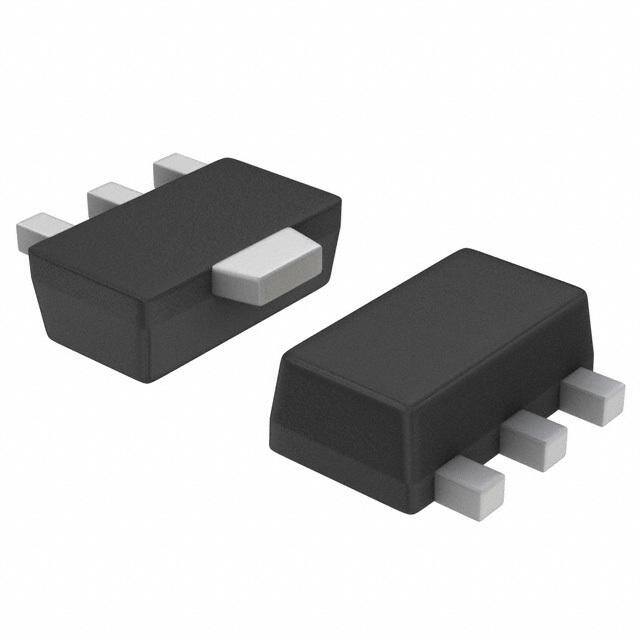
| 供应商器件封装 | SOT-89-3 |
| 其它名称 | MC78LC50HT1GOSDKR |
| 包装 | Digi-Reel® |
| 商标 | ON Semiconductor |
| 回动电压—最大值 | 38 mV at 1 mA |
| 安装类型 | 表面贴装 |
| 安装风格 | SMD/SMT |
| 封装 | Reel |
| 封装/外壳 | TO-243AA |
| 封装/箱体 | SOT-89-3 |
| 工作温度 | -40°C ~ 85°C |
| 工厂包装数量 | 1000 |
| 最大功率耗散 | 0.3 W |
| 最大工作温度 | + 85 C |
| 最大输入电压 | 12 V |
| 最小工作温度 | - 40 C |
| 标准包装 | 1 |
| 电压-跌落(典型值) | 0.03V @ 1mA |
| 电压-输入 | 最高 12V |
| 电压-输出 | 5V |
| 电压调节准确度 | 2.5 % |
| 电流-输出 | 80mA |
| 电流-限制(最小值) | - |
| 稳压器拓扑 | 正,固定式 |
| 稳压器数 | 1 |
| 系列 | MC78LC |
| 线路调整率 | 0.2 % / V |
| 负载调节 | 90 mV |
| 输入偏压电流—最大 | 0.001 mA |
| 输出电压 | 5 V |
| 输出电流 | 80 mA |
| 输出端数量 | 1 Output |
| 输出类型 | Fixed |

.jpg)


PDF Datasheet 数据手册内容提取
MC78LC00 Series Micropower Voltage Regulator The MC78LC00 series of fixed output low dropout linear regulators are designed for handheld communication equipment and portable battery powered applications which require low quiescent current. The MC78LC00 series features an ultra−low quiescent current of 1.1 (cid:2)A. www.onsemi.com Each device contains a voltage reference unit, an error amplifier, a PMOS power transistor, and resistors for setting output voltage. MARKING DIAGRAMS AND The MC78LC00 has been designed to be used with low cost ceramic PIN CONNECTIONS capacitors and requires a minimum output capacitor of 0.1 (cid:2)F. The device is housed in the micro−miniature Thin SOT23−5 surface mount package and SOT−89, 3 pin. Standard voltage versions are 1.5, 1.8, 5 GND 1 5 N/C X 2.5, 2.7, 2.8, 3.0, 3.3, 4.0, and 5.0 V. Other voltages are available in X X 100 mV steps. 1 Vin 2 (cid:2)AY TSOP−5 W Features NTR SUFFIX Vout 3 (cid:2) 4 N/C CASE 483 • Low Quiescent Current of 1.1 (cid:2)A Typical (Top View) • Excellent Line and Load Regulation • XXX= Specific Device Code Maximum Operating Voltage of 12 V A = Assembly Location • Low Output Voltage Option Y = Year • W = Work Week High Accuracy Output Voltage of 2.5% (cid:2) = Pb−Free Package • Industrial Temperature Range of −40°C to 85°C (Note: Microdot may be in either location) • Two Surface Mount Packages (SOT−89, 3 Pin, or SOT−23, 5 Pin) • These are Pb−Free Devices TAB GND 1 Typical Applications 1 XX • Vin 2 DD Tab Battery Powered Instruments SOT−89 • Hand−Held Instruments H SUFFIX Vout 3 CASE 1213 • Camcorders and Cameras (Top View) (Tab is connected to Pin 2) XX = Specific Device Code DD = Date Code 2 3 Vin VO ORDERING INFORMATION See detailed ordering and shipping information in the package dimensions section on page 10 of this data sheet. Vref 1 GND This device contains 8 active transistors. Figure 1. Representative Block Diagram © Semiconductor Components Industries, LLC, 2016 1 Publication Order Number: August, 2016 − Rev. 11 MC78LC00/D
MC78LC00 Series ÁÁÁÁÁÁÁÁÁÁÁÁÁÁÁÁÁÁÁÁÁÁÁÁÁÁÁÁÁÁÁÁÁ PIN FUNCTION DESCRIPTION ÁÁÁÁÁÁÁÁÁÁÁÁÁÁÁÁÁÁÁÁÁÁÁÁÁÁÁÁÁÁÁÁÁÁÁÁÁÁÁÁÁÁÁÁÁÁÁÁÁÁÁÁÁÁÁÁÁÁÁÁÁÁÁÁÁÁÁÁ ÁÁÁÁPÁÁin NÁÁo. ÁÁÁÁÁÁPÁÁin NÁÁameÁÁÁÁÁÁÁÁÁÁÁÁÁÁÁÁÁÁÁÁÁÁÁÁÁÁDÁÁescrÁÁiptioÁÁn ÁÁÁÁÁÁÁÁÁÁÁÁÁÁÁÁÁÁÁÁ 1 GND Power supply ground ÁÁÁÁÁÁÁÁÁÁÁÁÁÁÁÁÁÁÁÁÁÁÁÁÁÁÁÁÁÁÁÁÁÁÁÁÁÁÁÁÁÁÁÁÁÁÁÁÁÁÁÁÁÁÁÁÁÁÁÁÁÁÁÁÁÁÁÁÁÁ ÁÁÁÁÁÁ2ÁÁÁÁÁÁÁÁÁÁVÁÁin ÁÁÁÁÁÁPÁÁositiÁÁve pÁÁowerÁÁ supÁÁply iÁÁnputÁÁ voltÁÁageÁÁÁÁÁÁÁÁÁÁÁÁÁÁÁÁÁÁÁÁÁÁÁÁÁÁÁÁÁÁ ÁÁÁÁÁÁ3ÁÁÁÁÁÁÁÁÁÁVoÁÁut ÁÁÁÁÁÁRÁÁeguÁÁlatedÁÁ OutÁÁputÁÁÁÁÁÁÁÁÁÁÁÁÁÁÁÁÁÁÁÁÁÁÁÁÁÁÁÁÁÁÁÁÁÁÁÁÁÁ 4 N/C No Internal Connection ÁÁÁÁÁÁÁÁÁÁÁÁÁÁÁÁÁÁÁÁÁÁÁÁÁÁÁÁÁÁÁÁÁÁÁÁÁÁÁÁÁÁÁÁÁÁÁÁÁÁÁÁÁÁÁÁÁÁÁÁÁÁÁÁÁÁÁÁÁÁ 5 N/C No Internal Connection ÁÁÁÁÁÁÁÁÁÁÁÁÁÁÁÁÁÁÁÁÁÁÁÁÁÁÁÁÁÁÁÁÁÁÁ MAXIMUM RATINGS ÁÁÁÁÁÁÁÁÁRÁatingÁÁÁÁÁÁÁÁÁÁÁSyÁmboÁl ÁÁÁÁÁVaÁlue ÁÁÁÁÁUÁnit Á ÁÁÁÁInpuÁÁt VoÁÁltageÁÁÁÁÁÁÁÁÁÁÁÁÁÁÁÁÁÁÁÁÁÁÁÁÁÁÁÁÁÁÁÁÁÁÁÁVin ÁÁÁÁÁÁÁÁÁÁÁÁ1ÁÁ2 ÁÁÁÁÁÁÁÁÁÁÁÁV ÁÁ ÁÁOutÁput VÁoltaÁge ÁÁÁÁÁÁÁÁÁÁÁÁÁÁÁÁVÁoutÁÁÁÁÁ−0.Á3 to ÁVin +Á0.3ÁÁÁÁÁV Á Power Dissipation and Thermal Characteristics Case 483−01 (Thin SOT23−5) NTR Suffix Power Dissipation @ TA = 85°C PD 140 mW Thermal Resistance, Junction−to−Ambient R(cid:3)JA 280 °C/W Case 1213 (SOT−89) H Suffix Power Dissipation @ TA = 25°C PD 900 mW Thermal Resistance, Junction−to−Ambient R(cid:3)JA 111 °C/W ÁÁÁÁÁÁÁÁÁÁÁÁÁÁÁÁÁÁÁÁÁÁÁÁÁÁÁÁÁÁÁÁÁÁÁÁ Operating Junction Temperature TJ +125 °C ÁÁÁÁÁÁÁÁÁÁÁÁÁÁÁÁÁÁÁÁÁÁÁÁÁÁÁÁÁÁÁÁÁÁÁÁÁÁÁÁÁÁÁÁÁÁÁÁÁÁÁÁÁÁÁÁÁÁÁÁÁÁÁÁÁÁÁÁÁÁÁÁ Operating Ambient Temperature TA −40 to +85 °C ÁÁÁÁÁÁÁÁÁÁÁÁÁÁÁÁÁÁÁÁÁÁÁÁÁÁÁÁÁÁÁÁÁÁÁÁÁÁÁÁÁÁÁÁÁÁÁÁÁÁÁÁÁÁÁÁÁÁÁÁÁÁÁÁÁÁÁÁÁÁÁÁ Storage Temperature Tstg −55 to +150 °C ÁÁÁÁÁÁÁÁÁÁÁÁÁÁÁÁÁÁÁÁÁÁÁÁÁÁÁÁÁÁÁÁÁÁÁÁÁÁÁÁÁÁÁÁÁÁÁÁÁÁÁÁÁÁÁÁÁÁÁÁÁÁÁÁÁÁÁÁÁÁÁÁ Lead Soldering Temperature @ 260°C Tsolder 10 sec ÁÁÁÁÁÁÁÁÁÁÁÁÁÁÁÁÁÁÁÁÁÁÁÁÁÁÁÁÁÁÁÁÁÁÁÁ Stresses exceeding those listed in the Maximum Ratings table may damage the device. If any of these limits are exceeded, device functionality should not be assumed, damage may occur and reliability may be affected. www.onsemi.com 2
MC78LC00 Series ELECTRICAL CHARACTERISTICS (Vin = Vout(nom.) + 1.0 V, Cin = 1.0 (cid:2)F, Cout = 1.0 (cid:2)F, TJ = 25°C, unless otherwise noted.) (Note 5) NTR SUFFIX Characteristic Symbol Min Typ Max Unit Output Voltage (T = 25°C, I = 1.0 mA) V V A out out 1.5 V 1.455 1.5 1.545 1.8 V 1.746 1.8 1.854 2.5 V 2.425 2.5 2.575 2.7 V 2.646 2.7 2.754 2.8 V 2.744 2.8 2.856 3.0 V 2.94 3.0 3.06 3.3 V 3.234 3.3 3.366 4.0 V 3.9 4.0 4.1 5.0 V 4.90 5.0 5.10 Output Voltage (T = −40°C to 85°C) V V A out 1.5 V 1.455 1.5 1.545 1.8 V 1.746 1.8 1.854 2.5 V 2.425 2.5 2.575 2.7 V 2.619 2.7 2.781 2.8 V 2.716 2.8 2.884 3.0 V 2.910 3.0 3.09 3.3 V 3.201 3.3 3.399 4.0 V 3.9 4.0 4.1 5.0 V 4.90 5.0 5.10 Line Regulation (Vin = VO(nom.) + 1.0 V to 12 V, Iout = 1.0 mA) Regline − 0.05 0.2 %/V Load Regulation (I = 1.0 mA to 10 mA) Reg − 40 60 mV out load Output Current (Note 6) Iout mA 1.5 V, 1.8 V (Vin = 4.0 V) 35 50 − 2.5 V, 2.7 V, 2.8 V, 3.0 V (Vin = 5.0 V) 50 80 − 3.3 V (Vin = 6.0 V) 50 80 − 4.0 V (Vin = 7.0 V) 80 80 − 5.0 V (Vin = 8.0 V) 80 100 − Dropout Voltage (Iout = 1.0 mA, Measured at Vout −3.0%) Vin−Vout mV 1.5 V − 35 70 1.6 V−3.2 V − 30 60 3.3 V−3.9 V − 30 53 4.0 V−5.0 V − 30 38 Quiescent Current (Iout = 1.0 mA to IO(nom.)) IQ − 1.1 3.6 (cid:2)A Output Voltage Temperature Coefficient Tc − (cid:2)100 − ppm/°C Output Noise Voltage (f = 1.0 kHz to 100 kHz) V − 89 − (cid:2)Vrms n 1. This device series contains ESD protection and exceeds the following tests: Human Body Model 2000 V per MIL−STD−883, Method 3015 Machine Model Method 200 V 2. Latch up capability (85°C) (cid:2)100 mA 3. Maximum package power dissipation limits must be observed. TJ(max)(cid:4)TA PD(cid:3) R(cid:3)JA 4. Low duty cycle pulse techniques are used during testing to maintain the junction temperature as close to ambient as possible. 5. Low duty pulse techniques are used during test to maintain junction temperature as close to ambient as possible. 6. Output Current is measured when Vout = VO1 − 3% where VO1 = Vout at Iout = 0 mA. www.onsemi.com 3
MC78LC00 Series ELECTRICAL CHARACTERISTICS (Vin = Vout(nom.) + 1.0 V, Cin = 1.0 (cid:2)F, Cout = 1.0 (cid:2)F, TJ = 25°C, unless otherwise noted.) (Note 11) HT SUFFIX Characteristic Symbol Min Typ Max Unit Output Voltage V 30HT1 Suffix (Vin = 5.0 V) 2.950 3.0 3.075 33HT1 Suffix (Vin = 5.0 V) 3.218 3.3 3.382 40HT1 Suffix (Vin = 6.0 V) 3.900 4.0 4.100 ÁÁ5Á0HTÁ1 SÁuffix Á(Vin Á= 7.0Á V)ÁÁÁÁÁÁÁÁÁÁÁÁÁÁÁÁ4.87Á5 ÁÁÁÁ5.0 ÁÁÁÁ5.12Á5 ÁÁÁÁ Line Regulation Regline − 0.05 0.2 %/V ÁÁÁÁVÁÁin =ÁÁ [VOÁÁ + 1.ÁÁ0] VÁÁ to 1ÁÁ0 V, ÁÁIO = ÁÁ1.0 mÁÁA ÁÁÁÁÁÁÁÁÁÁÁÁÁÁÁÁÁÁÁÁÁÁÁÁÁÁÁÁÁÁÁÁÁÁÁÁÁÁÁÁÁÁÁÁÁÁÁÁÁÁÁÁÁÁ ÁÁLoaÁd ReÁgulaÁtion Á(IO =Á 1.0Á to 1Á0 mAÁ) ÁÁÁÁÁÁÁÁÁRÁegloÁad ÁÁÁÁÁÁÁÁÁÁÁÁÁÁÁÁmVÁ ÁÁ3Á0HTÁ1 SÁuffix Á(Vin Á= 5.0Á V)ÁÁÁÁÁÁÁÁÁÁÁÁÁÁÁÁ−ÁÁÁÁÁ40 ÁÁÁÁ60ÁÁÁÁÁ 33HT1 Suffix (Vin = 6.0 V) − 40 60 ÁÁ4Á0HTÁ1 SÁuffix Á(Vin Á= 7.0Á V)ÁÁÁÁÁÁÁÁÁÁÁÁÁÁÁÁ−ÁÁÁÁÁ50 ÁÁÁÁ70ÁÁÁÁÁ 50HT1 Suffix (Vin = 8.0 V) − 60 90 ÁÁÁÁÁÁÁÁÁÁÁÁÁÁÁÁÁÁÁÁÁÁÁÁÁÁÁÁÁÁÁÁÁÁÁÁÁÁÁÁÁÁÁÁÁÁÁÁÁÁÁÁÁÁÁÁÁÁÁÁÁÁÁÁÁÁÁÁÁÁÁÁÁÁÁÁ Output Current (Note 12) IO mA ÁÁ3Á0HTÁ1 SÁuffix Á(Vin Á= 5.0Á V)ÁÁÁÁÁÁÁÁÁÁÁÁÁÁÁÁ35ÁÁÁÁÁ50 ÁÁÁÁ−ÁÁÁÁÁ 33HT1 Suffix (Vin = 6.0 V) 35 50 − ÁÁ4Á0HTÁ1 SÁuffix Á(Vin Á= 7.0Á V)ÁÁÁÁÁÁÁÁÁÁÁÁÁÁÁÁ45ÁÁÁÁÁ65 ÁÁÁÁ−ÁÁÁÁÁ ÁÁÁÁ5ÁÁ0HTÁÁ1 SÁÁuffix ÁÁ(Vin ÁÁ= 8.0ÁÁ V)ÁÁÁÁÁÁÁÁÁÁÁÁÁÁÁÁÁÁÁÁÁÁÁÁÁÁÁÁÁÁÁÁ55ÁÁÁÁÁÁÁÁÁÁ80 ÁÁÁÁÁÁÁÁ−ÁÁÁÁÁÁÁÁÁÁ Dropout Voltage Vin − VO mV ÁÁ3Á0HTÁ1 SÁuffix Á(IO =Á 1.0Á mAÁ) ÁÁÁÁÁÁÁÁÁÁÁÁÁÁÁ−ÁÁÁÁÁ40 ÁÁÁÁ60ÁÁÁÁÁ ÁÁ3Á3HTÁ1 SÁuffix Á(IO =Á 1.0Á mAÁ) ÁÁÁÁÁÁÁÁÁÁÁÁÁÁÁ−ÁÁÁÁÁ35 ÁÁÁÁ53ÁÁÁÁÁ 40HT1 Suffix (IO = 1.0 mA) − 25 38 ÁÁÁÁ5ÁÁ0HTÁÁ1 SÁÁuffix ÁÁ(IO =ÁÁ 1.0ÁÁ mAÁÁ) ÁÁÁÁÁÁÁÁÁÁÁÁÁÁÁÁÁÁÁÁÁÁÁÁÁÁÁÁÁÁ−ÁÁÁÁÁÁÁÁÁÁ25 ÁÁÁÁÁÁÁÁ38ÁÁÁÁÁÁÁÁÁÁ ÁÁQuiÁesceÁnt CÁurrenÁt ÁÁÁÁÁÁÁÁÁÁÁÁÁÁICCÁÁÁÁÁÁÁÁÁÁÁÁÁÁÁÁÁ(cid:2)AÁ 30HT1 Suffix (Vin = 5.0 V) − 1.1 3.3 ÁÁ3Á3HTÁ1 SÁuffix Á(Vin Á= 5.0Á V)ÁÁÁÁÁÁÁÁÁÁÁÁÁÁÁÁ−ÁÁÁÁÁ1.1 ÁÁÁÁ3.3ÁÁÁÁÁ 40HT1 Suffix (Vin = 6.0 V) − 1.2 3.6 ÁÁÁÁ5ÁÁ0HTÁÁ1 SÁÁuffix ÁÁ(Vin ÁÁ= 7.0ÁÁ V)ÁÁÁÁÁÁÁÁÁÁÁÁÁÁÁÁÁÁÁÁÁÁÁÁÁÁÁÁÁÁÁÁ−ÁÁÁÁÁÁÁÁÁÁ1.3 ÁÁÁÁÁÁÁÁ3.9ÁÁÁÁÁÁÁÁÁÁ ÁÁOutÁput VÁoltaÁge TÁempÁeratuÁre CÁoeffÁicienÁt ÁÁÁÁÁÁÁÁÁTCÁÁÁÁ−ÁÁÁÁ±Á100ÁÁÁÁ−ÁÁÁpÁpm/Á°C 7. This device series contains ESD protection and exceeds the following tests: Human Body Model 2000 V per MIL−STD−883, Method 3015 Machine Model Method 200 V 8. Latch up capability (85°C) (cid:2)100 mA 9. Maximum package power dissipation limits must be observed. TJ(max)(cid:4)TA PD(cid:3) R(cid:3)JA 10.Low duty cycle pulse techniques are used during testing to maintain the junction temperature as close to ambient as possible. 11.Low duty pulse techniques are used during test to maintain junction temperature as close to ambient as possible. 12.Output Current is measured when Vout = VO1 − 3% where VO1 = Vout at Iout = 0 mA. DEFINITIONS Load Regulation difference between the input current (measured through the The change in output voltage for a change in output current LDO input pin) and the output current. at a constant temperature. Line Regulation Dropout Voltage The change in output voltage for a change in input voltage. The input/output differential at which the regulator output The measurement is made under conditions of low dissipation no longer maintains regulation against further reductions in or by using pulse technique such that the average chip input voltage. Measured when the output drops 3% below its temperature is not significantly affected. nominal. The junction temperature, load current, and Line Transient Response minimum input supply requirements affect the dropout level. Typical over and undershoot response when input voltage is Maximum Power Dissipation excited with a given slope. The maximum total dissipation for which the regulator will Maximum Package Power Dissipation operate within its specifications. The maximum power package dissipation is the power Quiescent Current dissipation level at which the junction temperature reaches its The quiescent current is the current which flows through the maximum operating value, i.e. 125°C. Depending on the ground when the LDO operates without a load on its output: ambient power dissipation and thus the maximum available internal IC operation, bias, etc. When the LDO becomes output current. loaded, this term is called the Ground current. It is actually the www.onsemi.com 4
MC78LC00 Series 3.2 3.2 TA = 25°C NTR Series 3.1 GE (V) 2.93 IO = 1 mA AGE (V)3.0 IO = 1.0 mA LTA 2.8 IO = 10 mA OLT2.8 PUT VO 22..67 IO = 5 mA TPUT V2.6 IO = 5.0 mA T U U 2.5 O , OO 2.4 V, O2.4 MC78LC30HT1 V 2.3 TA = 25°C IO = 10 mA 2.2 2.2 2.5 2.7 2.9 3.1 3.3 3.5 2.5 2.7 2.9 3.1 3.3 3.5 Vin, Input Voltage (V) Vin, Input Voltage (V) Figure 2. Output Voltage versus Input Voltage Figure 3. Output Voltage versus Input Voltage 3.05 3.2 NTR Series 3 −40°C 3.1 GE (V)22.9.95 80°C AGE (V) 3.0 TA = −30°C A T T L L2.85 O T VO 2.8 UT V 2.9 TPU2.75 25°C UTP 2.8 TA = 25°C U O V, OO22.6.75 V, O2.7 MC78LC30HT1 TA = 80°C 2.6 0 0 20 40 60 80 100 120 0 20 40 60 80 100 120 IO, Output Current (mA) IO, Output Current (mA) Figure 4. Output Voltage versus Output Current Figure 5. Output Voltage versus Output Current 2 2.0 V) 1.8 MC78LC30NTR V) GE ( 1.6 TA = 25°C GE ( 1.6 A A LT 1.4 LT O O V 1.2 V T T 1.2 U 1 U O O P P O 0.8 O R R 0.8 D 0.6 D , O , O V 0.4 V MC78LC30HT1 − − 0.4 V in 0.2 V in TA = 25°C 0 0 0 10 20 30 40 50 0 10 20 30 40 50 IO, Output Current (mA) IO, Output Current (mA) Figure 6. Dropout Voltage versus Output Current Figure 7. Dropout Voltage versus Output Current www.onsemi.com 5
MC78LC00 Series 3.1 3.10 MC78LC30NTR Vin = 5.0 V V) 3.06 Vin = 4.0 V V) 3.06 IO = 10 mA E ( IO = 10 mA E ( G G A A LT3.02 LT 3.02 O O V V T T PU2.98 PU 2.98 T T U U O O MC78LC30HT1 , O2.94 , O2.94 V V 2.9 2.90 −40 −20 0 20 40 60 80 −40 −20 0 20 40 60 80 TA, Ambient Temperature (°C) TA, Ambient Temperature (°C) Figure 8. Output Voltage versus Temperature Figure 9. Output Voltage versus Temperature 1.4 1.4 MC78LC30NTR TA = 25°C (cid:2)A) 1.3 TA = 25°C (cid:2)A) 1.3 T ( IO = 0 mA T ( N N RE 1.2 RE 1.2 R R U U C C T 1.1 T 1.1 N N E E C C S 1 S 1.0 E E UI UI MC78LC30HT1 , QQ 0.9 , QQ 0.9 I I 0.8 0.8 3 4 5 6 7 8 9 10 11 12 3.0 4.0 5.0 6.0 7.0 8.0 9.0 10 Vin, Input Voltage (V) Vin, Input Voltage (V) Figure 10. Quiescent Current versus Input Voltage Figure 11. Quiescent Current versus Input Voltage 1.75 1.2 MC78LC30NTR Vin = 5.0 V (cid:2)A) 1.5 Vin = 4.0 V (cid:2)A) 1.1 T ( IO = 0 mA T ( N N E E 1.0 R R R1.25 R U U C C 0.9 T T EN 1 EN C C 0.8 S S E E QUI0.75 QUI 0.7 MC78LC30HT1 , Q , Q I I 0.5 0.6 −20 0 20 40 60 80 −40 −20 0 20 40 60 80 TA, Ambient Temperature (°C) TA, Ambient Temperature (°C) Figure 12. Quiescent Current versus Temperature Figure 13. Quiescent Current versus Temperature www.onsemi.com 6
MC78LC00 Series 0.8 0.8 V) 0.7 NTR Series V)0.7 HT1 Series E ( E ( IO = 10 mA G G A 0.6 A0.6 T T L L O 0.5 O0.5 V V T T U 0.4 U0.4 O O P P O 0.3 O0.3 R R D D ut, 0.2 ut,0.2 − Vo 0.1 − Vo0.1 IO = 1.0 mA n n Vi Vi 0 0 0.0 1.0 2.0 3.0 4.0 5.0 6.0 0 1.0 2.0 3.0 4.0 5.0 6.0 VO, Set Output Voltage (V) VO, Set Output Voltage (V) Figure 14. Dropout Voltage versus Set Output Voltage Figure 15. Dropout Voltage versus Set Output Voltage age (V) 6.0 NTR Series AGE (V) 87..05 olt 5.0 LT Input Voltage V O 7.0 put T V n 4.0 U 6.5 I P 300 Vin = 4.5 V to 5.5 V RL = 3 k OUT 6.0 geV) 200 Vout = 3.0 V Cout = 0.1 (cid:2)F E/ ut Voltaation (m 1000 OLTAG 55..50 HT1 Series Output Voltage OutpDevi−−120000 PUT V 4.5 CIOO = = 1 0.0.1 m (cid:2)AF N −300 I 4.0 0 0.5 1.0 1.5 2.0 2.5 0 2.0 4.0 6.0 Time (mS) t, Time (ms) Figure 16. Line Transient Figure 17. Line Transient Response 3.5 1.5 GE (V) 32..05 TA = 25°C NTR Series (cid:2)T (A) 1.0 TIOA == 02 5m°AC NTR Series 50 (cid:2)A TA EN 0.8 200 (cid:2)A L R O 2.0 R T V CU 0.6 50 (cid:2)A OUTPU 11..50 IO = 50 (cid:2)A OUND 0.4 100 (cid:2)A , ut 100 (cid:2)A GR Vo0.5 I g 0.2 200 (cid:2)A 200 (cid:2)A 0 0 0 0.5 1.0 1.5 2.0 2.5 0 0.5 1.0 1.5 2.0 2.5 Vin, Input Voltage (V) Vin, Input Voltage (V) Figure 18. Output Voltage versus Input Voltage Figure 19. Ground Current versus Input Voltage www.onsemi.com 7
MC78LC00 Series APPLICATIONS INFORMATION A typical application circuit for the MC78LC00 series is Thermal shown in Figure 20. As power across the MC78LC00 increases, it might become necessary to provide some thermal relief. The Input Decoupling (C1) maximum power dissipation supported by the device is A 0.1 (cid:2)F capacitor either ceramic or tantalum is dependent upon board design and layout. Mounting pad recommended and should be connected close to the configuration on the PCB, the board material, and also the MC78LC00 package. Higher values and lower ESR will ambient temperature effect the rate of temperature rise for improve the overall line transient response. the part. This is stating that when the MC78LC00 has good thermal conductivity through the PCB, the junction Output Decoupling (C2) temperature will be relatively low with high power The MC78LC00 is a stable component and does not dissipation applications. require any specific Equivalent Series Resistance (ESR) or The maximum dissipation the package can handle is a minimum output current. Capacitors exhibiting ESRs given by: ranging from a few m(cid:4) up to 3.0 (cid:4) can thus safely be used. The minimum decoupling value is 0.1 (cid:2)F and can be TJ(max)(cid:4)TA PD(cid:3) augmented to fulfill stringent load transient requirements. R(cid:3)JA The regulator accepts ceramic chip capacitors as well as If junction temperature is not allowed above the tantalum devices. Larger values improve noise rejection and maximum 125°C, then the MC78LC00NTR can dissipate load regulation transient response. up to 357 mW @ 25°C. The power dissipated by the MC78LC00NTR can be Hints calculated from the following equation: Please be sure the Vin and GND lines are sufficiently wide. When the impedance of these lines is high, there is a Ptot(cid:3)(cid:5)Vin*Ignd(Iout)(cid:6)(cid:7)[Vin(cid:4)Vout]*Iout chance to pick up noise or cause the regulator to or malfunction. as Scelot seex atesr pnoals sciobmle ptoo nthene tcsi, recsupite,c ainaldl ym tahkee o luetapdust acsa sphaocritt oars, VinMAX(cid:3)PtoItg(cid:7)ndV(cid:7)ouIto*uItout possible. If an 80 mA output current is needed then the ground current from the data sheet is 1.1 (cid:2)A. For an MC78LC30NTR (3.0 V), the maximum input voltage will then be 7.4 V. Battery or Unregulated Voltage + C1 + Vout C2 Figure 20. Basic Application Circuit for NTR Suffixes www.onsemi.com 8
MC78LC00 Series MJD32C 0.033 (cid:2)F 2 3 100 2 3 Vin MC78LC00 VO Vin MC78LC00 VO R1 C2 1 0.1 (cid:2)F 1 0.1 (cid:2)F C1 ICC GND R2 GND GND Figure 21. Current Boost Circuit Figure 22. Adjustable V O MJD32C R2 Q1 Q2 0.033 (cid:2)F MMBT2907 ALT1 2 3 Vin MC78LC00 VO R1 1 0.1 (cid:2)F 0.1 (cid:2)F GND GND Figure 23. Current Boost Circuit with Overcurrent Limit Circuit (cid:9) (cid:10) VO (cid:3) VO(Reg) 1 (cid:7) RR21 (cid:7) ICCR2 IO(shortcircuit) (cid:8) VRBE22 (cid:7) VBE1R(cid:7)1VBE2 www.onsemi.com 9
MC78LC00 Series ORDERING INFORMATION Nominal Device Output Voltage Marking Package Shipping† MC78LC15NTRG 1.5 LAG MC78LC18NTRG 1.8 LAH MC78LC25NTRG 2.5 LAI MC78LC27NTRG 2.7 LAJ Thin SOT23−5 MC78LC28NTRG 2.8 LAK 3000 Units/7″ Tape & Reel (Pb−Free) MC78LC30NTRG 3.0 LAL MC78LC33NTRG 3.3 LAM MC78LC40NTRG 4.0 LEC MC78LC50NTRG 5.0 LAN MC78LC30HT1G 3.0 0C MC78LC33HT1G 3.3 3C SOT−89 1000 Units Tape & Reel (Pb−Free) MC78LC40HT1G 4.0 0D MC78LC50HT1G 5.0 0E †For information on tape and reel specifications, including part orientation and tape sizes, please refer to our Tape and Reel Packaging Specifications Brochure, BRD8011/D. Additional voltages in 100 mV steps are available upon request by contacting your ON Semiconductor representative. www.onsemi.com 10
MC78LC00 Series PACKAGE DIMENSIONS TSOP−5 (SOT23−5) NTR SUFFIX CASE 483 ISSUE M NOTES: 1. DIMENSIONING AND TOLERANCING PER ASME NOTE 5 D5X Y14.5M, 1994. 2. CONTROLLING DIMENSION: MILLIMETERS. 0.20 C A B 3. MAXIMUM LEAD THICKNESS INCLUDES LEAD FINISH 2X 0.10 T THICKNESS. MINIMUM LEAD THICKNESS IS THE MINIMUM THICKNESS OF BASE MATERIAL. M 4. DIMENSIONS A AND B DO NOT INCLUDE MOLD 2X 0.20 T B 5 4 S FFLLAASSHH,, PPRROOTTRRUUSSIIOONNSS,, OORR GGAATTEE BBUURRRRSS. SMHOALLDL NOT 1 2 3 EXCEED 0.15 PER SIDE. DIMENSION A. K 5. OPTIONAL CONSTRUCTION: AN ADDITIONAL B G DETAIL Z TTRRIIMMMMEEDD LLEEAADD INSO ATL TLOO WEXETDE INND T HMIOS RLEO CTHATAINO N0..2 A A FROM BODY. MILLIMETERS TOP VIEW DIM MIN MAX A 2.85 3.15 B 1.35 1.65 DETAIL Z C 0.90 1.10 J D 0.25 0.50 C G 0.95 BSC H 0.01 0.10 0.05 J 0.10 0.26 H C SPELAATNIENG END VIEW MK 0.02 0(cid:3) 010.6 (cid:3) 0 SIDE VIEW S 2.50 3.00 SOLDERING FOOTPRINT* 1.9 0.074 0.95 0.037 2.4 0.094 1.0 0.039 0.7 (cid:9) (cid:10) 0.028 SCALE 10:1 mm inches *For additional information on our Pb−Free strategy and soldering details, please download the ON Semiconductor Soldering and Mounting Techniques Reference Manual, SOLDERRM/D. www.onsemi.com 11
MC78LC00 Series PACKAGE DIMENSIONS SOT−89 H SUFFIX CASE 1213−02 ISSUE C NOTES: −A− C 1. DIMENSIONING AND TOLERANCING PER ANSI J Y14.5M, 1982. F 2. CONTROLLING DIMENSION: MILLIMETERS 3. 1213-01 OBSOLETE, NEW STANDARD 1213-02. MILLIMETERS INCHES DIM MIN MAX MIN MAX L −B− A 4.40 4.60 0.173 0.181 B 2.40 2.60 0.094 0.102 C 1.40 1.60 0.055 0.063 K D 0.37 0.57 0.015 0.022 E 0.32 0.52 0.013 0.020 D F 1.50 1.83 0.059 0.072 0.10 M T B S A S −T− SPELAATNIENG G 1.50 BSC 0.059 BSC H 3.00 BSC 0.118 BSC E 2 PL KJ 00..3800 0-.-5-0 00..001321 0.0-2-0- G 0.10 M T B S A S L --- 4.25 --- 0.167 H ON Semiconductor and are trademarks of Semiconductor Components Industries, LLC dba ON Semiconductor or its subsidiaries in the United States and/or other countries. ON Semiconductor owns the rights to a number of patents, trademarks, copyrights, trade secrets, and other intellectual property. A listing of ON Semiconductor’s product/patent coverage may be accessed at www.onsemi.com/site/pdf/Patent−Marking.pdf. ON Semiconductor reserves the right to make changes without further notice to any products herein. ON Semiconductor makes no warranty, representation or guarantee regarding the suitability of its products for any particular purpose, nor does ON Semiconductor assume any liability arising out of the application or use of any product or circuit, and specifically disclaims any and all liability, including without limitation special, consequential or incidental damages. Buyer is responsible for its products and applications using ON Semiconductor products, including compliance with all laws, regulations and safety requirements or standards, regardless of any support or applications information provided by ON Semiconductor. “Typical” parameters which may be provided in ON Semiconductor data sheets and/or specifications can and do vary in different applications and actual performance may vary over time. All operating parameters, including “Typicals” must be validated for each customer application by customer’s technical experts. ON Semiconductor does not convey any license under its patent rights nor the rights of others. ON Semiconductor products are not designed, intended, or authorized for use as a critical component in life support systems or any FDA Class 3 medical devices or medical devices with a same or similar classification in a foreign jurisdiction or any devices intended for implantation in the human body. Should Buyer purchase or use ON Semiconductor products for any such unintended or unauthorized application, Buyer shall indemnify and hold ON Semiconductor and its officers, employees, subsidiaries, affiliates, and distributors harmless against all claims, costs, damages, and expenses, and reasonable attorney fees arising out of, directly or indirectly, any claim of personal injury or death associated with such unintended or unauthorized use, even if such claim alleges that ON Semiconductor was negligent regarding the design or manufacture of the part. ON Semiconductor is an Equal Opportunity/Affirmative Action Employer. This literature is subject to all applicable copyright laws and is not for resale in any manner. PUBLICATION ORDERING INFORMATION LITERATURE FULFILLMENT: N. American Technical Support: 800−282−9855 Toll Free ON Semiconductor Website: www.onsemi.com Literature Distribution Center for ON Semiconductor USA/Canada 19521 E. 32nd Pkwy, Aurora, Colorado 80011 USA Europe, Middle East and Africa Technical Support: Order Literature: http://www.onsemi.com/orderlit Phone: 303−675−2175 or 800−344−3860 Toll Free USA/Canada Phone: 421 33 790 2910 Fax: 303−675−2176 or 800−344−3867 Toll Free USA/Canada Japan Customer Focus Center For additional information, please contact your local Email: orderlit@onsemi.com Phone: 81−3−5817−1050 Sales Representative www.onsemi.com MC78LC00/D 12
Mouser Electronics Authorized Distributor Click to View Pricing, Inventory, Delivery & Lifecycle Information: O N Semiconductor: MC78LC15NTR MC78LC15NTRG MC78LC18NTR MC78LC18NTRG MC78LC25NTR MC78LC25NTRG MC78LC27NTR MC78LC27NTRG MC78LC28NTR MC78LC28NTRG MC78LC30HT1 MC78LC30HT1G MC78LC30NTR MC78LC30NTRG MC78LC33HT1 MC78LC33HT1G MC78LC33NTR MC78LC33NTRG MC78LC40HT1 MC78LC40HT1G MC78LC40NTR MC78LC40NTRG MC78LC50HT1 MC78LC50HT1G MC78LC50NTR MC78LC50NTRG NCP78LC33NTRG NCP78LC27NTRG NCP78LC25NTRG NCP78LC50NTRG NCP78LC40NTRG NCP78LC30NTRG NCP78LC28NTRG