ICGOO在线商城 > 集成电路(IC) > PMIC - 稳压器 - 线性 > MC78L05ABDG

 Datasheet下载
- 型号: MC78L05ABDG
- 制造商: ON Semiconductor
- 库位|库存: xxxx|xxxx
- 要求:
| 数量阶梯 | 香港交货 | 国内含税 |
| +xxxx | $xxxx | ¥xxxx |
查看当月历史价格
查看今年历史价格
MC78L05ABDG产品简介:
ICGOO电子元器件商城为您提供MC78L05ABDG由ON Semiconductor设计生产,在icgoo商城现货销售,并且可以通过原厂、代理商等渠道进行代购。 MC78L05ABDG价格参考。ON SemiconductorMC78L05ABDG封装/规格:PMIC - 稳压器 - 线性, Linear Voltage Regulator IC Positive Fixed 1 Output 5V 100mA 8-SOIC。您可以下载MC78L05ABDG参考资料、Datasheet数据手册功能说明书,资料中有MC78L05ABDG 详细功能的应用电路图电压和使用方法及教程。
ON Semiconductor的MC78L05ABDG是一款低功耗、三端线性稳压器,属于PMIC(电源管理集成电路)中的线性稳压器类别。它具有固定的输出电压为5V,最大输出电流为100mA,并且具备过热保护和短路保护功能。这款器件广泛应用于各种需要稳定5V电源的低功耗场景中。

 应用场景:

1. 消费电子:
   - 便携式设备:如MP3播放器、智能手表、蓝牙耳机等。这些设备通常对功耗要求较高,MC78L05ABDG能够提供稳定的5V电源,同时保持低功耗,延长电池寿命。
   - 智能家居设备:如智能音箱、智能插座等。这些设备可能需要长时间工作,MC78L05ABDG的低功耗特性和稳定性可以确保设备在长时间运行时不会因电源问题而出现故障。

2. 工业控制:
   - 传感器模块:许多工业传感器(如温度传感器、湿度传感器)需要稳定的5V电源供电,MC78L05ABDG可以为这些传感器提供可靠的电源支持,确保数据采集的准确性。
   - PLC(可编程逻辑控制器):在工业自动化系统中,PLC需要稳定的电源来保证其正常工作,MC78L05ABDG可以为其内部电路提供稳定的5V电源。

3. 通信设备:
   - 无线模块:如Wi-Fi模块、Zigbee模块等,这些模块通常需要5V电源供电,MC78L05ABDG可以为这些模块提供稳定的电源,确保通信的可靠性和稳定性。
   - 路由器和交换机:这些网络设备中的某些子模块(如接口芯片、处理器等)可能需要5V电源,MC78L05ABDG可以为这些模块提供稳定的电源支持。

4. 医疗设备:
   - 便携式医疗设备:如血糖仪、血氧仪等,这些设备通常体积小、功耗低,MC78L05ABDG可以为这些设备提供稳定的5V电源,确保测量结果的准确性。
   - 监护设备:如心率监测仪、血压计等,这些设备需要长时间工作,MC78L05ABDG的低功耗特性和稳定性可以确保设备在长时间使用过程中不会因为电源问题而影响性能。

总的来说,MC78L05ABDG适用于各种需要稳定5V电源的低功耗应用场景,特别是在便携式设备、工业控制、通信设备和医疗设备等领域表现出色。
| 参数 | 数值 |
| 产品目录 | 集成电路 (IC)半导体 |
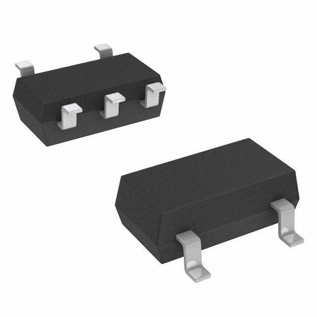
| 描述 | IC REG LDO 5V 0.1A 8SOIC线性稳压器 5V 100mA Postive |
| 产品分类 | |
| 品牌 | ON Semiconductor |
| 产品手册 | |
| 产品图片 |
|
| rohs | 符合RoHS无铅 / 符合限制有害物质指令(RoHS)规范要求 |
| 产品系列 | 电源管理 IC,线性稳压器,ON Semiconductor MC78L05ABDG- |
| 数据手册 | |
| 产品型号 | MC78L05ABDG |
| PCN组件/产地 | |
| PSRR/纹波抑制—典型值 | 49 dB |
| 产品目录页面 | |
| 产品种类 | 线性稳压器 |
| 供应商器件封装 | 8-SOIC N |
| 其它名称 | MC78L05ABDG-ND |
| 包装 | 管件 |
| 商标 | ON Semiconductor |
| 安装类型 | 表面贴装 |
| 安装风格 | SMD/SMT |
| 封装 | Tube |
| 封装/外壳 | 8-SOIC(0.154",3.90mm 宽) |
| 封装/箱体 | SOIC-8 |
| 工作温度 | -40°C ~ 125°C |
| 工厂包装数量 | 98 |
| 最大工作温度 | + 125 C |
| 最大输入电压 | 30 V |
| 最小工作温度 | - 40 C |
| 最小输入电压 | 7 V |
| 极性 | Positive |
| 标准包装 | 98 |
| 电压-跌落(典型值) | 1.7V @ 40mA |
| 电压-输入 | 最高 30V |
| 电压-输出 | 5V |
| 电流-输出 | 100mA |
| 电流-限制(最小值) | - |
| 稳压器拓扑 | 正,固定式 |
| 稳压器数 | 1 |
| 系列 | MC78L05A |
| 线路调整率 | 150 mV |
| 负载调节 | 60 mV |
| 输出电压 | 5 V |
| 输出电流 | 0.1 A |
| 输出端数量 | 1 |
| 输出类型 | Fixed |


PDF Datasheet 数据手册内容提取
MC78L00A Series, NCV78L00A 100 mA Positive Voltage Regulators The MC78L00A Series of positive voltage regulators are inexpensive, easy−to−use devices suitable for a multitude of www.onsemi.com applications that require a regulated supply of up to 100 mA. Like their higher powered MC7800 and MC78M00 Series cousins, these regulators feature internal current limiting and thermal shutdown making them remarkably rugged. No external components are required with the MC78L00 devices in many applications. These devices offer a substantial performance advantage over the traditional zener diode−resistor combination, as output impedance 1 and quiescent current are substantially reduced. 12 2 3 3 Features STRAIGHT LEAD BENT LEAD • BULK PACK TAPE & REEL Wide Range of Available, Fixed Output Voltages AMMO PACK • Low Cost TO−92 Pin: 1. Output • Internal Short Circuit Current Limiting P SUFFIX 2. Ground • CASE 029 3. Input Internal Thermal Overload Protection • No External Components Required • Complementary Negative Regulators Offered (MC79L00A Series) • NCV Prefix for Automotive and Other Applications Requiring SOIC−8* Unique Site and Control Change Requirements; AEC−Q100 D SUFFIX SOT−89 Qualified and PPAP Capable CASE 751 CASE 528AG • These are Pb−Free Devices *SOIC−8 is an internally modified SO−8 package. Pins 2, 3, 6, and 7 are electrically common to the die attach flag. This internal lead frame modification decreases Input package thermal resistance and increases power 15k Q3 Q5 Q11 dissipation capability when appropriately mounted on a printed circuit board. SOIC−8 conforms to all ex- Q12 ternal dimensions of the standard SO−8 package. Q1 Q10 PIN CONNECTIONS 3.8k 5.0k 3.0 Output Q4 Q6 VOUT 1 8 VIN 0-25k GND 2 7 GND GND 3 6 GND 1.9k 19k 2.2k 1.2k NC 4 5 NC Q9 C (Top View) Q8 Z1 Q2 2.85k TAB Q7 420 1.0k Ground 1 2 3 VOUTGND VIN (Top View) Figure 1. Representative Schematic Diagram ORDERING INFORMATION See detailed ordering and shipping information in the package dimensions section on page 9 of this data sheet. DEVICE MARKING INFORMATION See general marking information in the device marking section on page 12 of this data sheet. © Semiconductor Components Industries, LLC, 1999 1 Publication Order Number: October, 2016 − Rev. 18 MC78L00A/D
MC78L00A Series, NCV78L00A Input MC78LXXA Output 0.33C (cid:2)inF* C0.O1* (cid:2)*F Figure 2. Standard Application A common ground is required between the input and the output voltages. The input voltage must remain typically 2.0 V above the output voltage even during the low point on the input ripple voltage. * Cin is required if regulator is located an appreciable distance from power supply filter. **CO is not needed for stability; however, it does improve transient response. ABSOLUTE MAXIMUM RATINGS Rating Symbol Value Unit Input Voltage (5.0 V−9.0 V) VI 30 Vdc Input Voltage (12 V−18 V) 35 Input Voltage (24 V) 40 Storage Temperature Range Tstg −65 to +150 °C Maximum Junction Temperature TJ 150 °C Moisture Sensitivity Level MSL 1 − ESD Capability, Human Body Model (Note 1) ESDHBM 2000 V ESD Capability, Machine Model (Note 1) ESDMM 200 V ESD Capability, Charged Device Model (Note 1) ESDCDM 2000 V Stresses exceeding those listed in the Maximum Ratings table may damage the device. If any of these limits are exceeded, device functionality should not be assumed, damage may occur and reliability may be affected. 1. This device series incorporates ESD protection and is tested by the following methods: ESD Human Body Model tested per AEC−Q100−002 (EIA/JESD22−A114) ESD Machine Model tested per AEC−Q100−003 (EIA/JESD22−A115) ESD Charged Device Model tested per EIA/JES D22/C101, Field Induced Charge Model. THERMAL CHARACTERISTICS Rating Symbol Value Unit Package Dissipation PD Internally Limited W Thermal Characteristics, TO−92 R(cid:3)JA 200 °C/W Thermal Resistance, Junction−to−Ambient Thermal Characteristics, SOIC8 R(cid:3)JA Refer to Figure 8 °C/W Thermal Resistance, Junction−to−Ambient Thermal Characteristics, SOT−89 R(cid:3)JA 55 °C/W Thermal Resistance, Junction−to−Ambient 2. Thermal Resistance, Junction−to−Ambient depends on P.C.B. Copper area. See details in Figure 8. Thermal Resistance, Junction−to−Case is not defined. SOIC 8 lead and TO-92 packages that do not have a heat sink like other packages may have. This is the reason that a Theta JC is never specified. A little heat transfer will occur through the package but since it is plastic, it is minimal. The majority of the heat that is transferred is through the leads where they connect to the circuit board. www.onsemi.com 2
MC78L00A Series, NCV78L00A ELECTRICAL CHARACTERISTICS (VI = 10 V, IO = 40 mA, CI = 0.33 (cid:2)F, CO = 0.1 (cid:2)F, −40°C < TJ < +125°C (for MC78LXXAB, NCV78L05A), 0°C < TJ < +125°C (for MC78LXXAC), unless otherwise noted.) MC78L05AC, AB, NCV78L05A Characteristics Symbol Min Typ Max Unit Output Voltage (TJ = +25°C) VO 4.8 5.0 5.2 Vdc Line Regulation Regline mV (TJ = +25°C, IO = 40 mA) 7.0 Vdc ≤ VI ≤ 20 Vdc − 55 150 8.0 Vdc ≤ VI ≤ 20 Vdc − 45 100 Load Regulation Regload mV (TJ = +25°C, 1.0 mA ≤ IO ≤ 100 mA) − 11 60 (TJ = +25°C, 1.0 mA ≤ IO ≤ 40 mA) − 5.0 30 Output Voltage VO Vdc (7.0 Vdc ≤ VI ≤ 20 Vdc, 1.0 mA ≤ IO ≤ 40 mA) 4.75 − 5.25 (VI = 10 V, 1.0 mA ≤ IO ≤ 70 mA) 4.75 − 5.25 Input Bias Current IIB mA (TJ = +25°C) − 3.8 6.0 (TJ = +125°C) − − 5.5 Input Bias Current Change (cid:4)IIB mA (8.0 Vdc ≤ VI ≤ 20 Vdc) − − 1.5 (1.0 mA ≤ IO ≤ 40 mA) − − 0.1 Output Noise Voltage Vn − 40 − (cid:2)V (TA = +25°C, 10 Hz ≤ f≤ 100 kHz) Ripple Rejection (IO = 40 mA, RR 41 49 − dB f = 120 Hz, 8.0 Vdc ≤ VI ≤ 18 V, TJ = +25°C) Dropout Voltage (TJ = +25°C) VI − VO − 1.7 − Vdc NOTE: NCV78L05A: Tlow = −40°C, Thigh = +125°C. Guaranteed by design. NCV prefix is for automotive and other applications requiring site and change control. ELECTRICAL CHARACTERISTICS (VI = 14 V, IO = 40 mA, CI = 0.33 (cid:2)F, CO = 0.1 (cid:2)F, −40°C < TJ < +125°C (for MC78LXXAB), 0°C < TJ < +125°C (for MC78LXXAC), unless otherwise noted.) MC78L08AC, AB Characteristics Symbol Min Typ Max Unit Output Voltage (TJ = +25°C) VO 7.7 8.0 8.3 Vdc Line Regulation Regline mV (TJ = +25°C, IO = 40 mA) 10.5 Vdc ≤ VI ≤ 23 Vdc − 20 175 11 Vdc ≤ VI ≤ 23 Vdc − 12 125 Load Regulation Regload mV (TJ = +25°C, 1.0 mA ≤ IO ≤ 100 mA) − 15 80 (TJ = +25°C, 1.0 mA ≤ IO ≤ 40 mA) − 8.0 40 Output Voltage VO Vdc (10.5 Vdc ≤ VI ≤ 23 Vdc, 1.0 mA ≤ IO ≤ 40 mA) 7.6 − 8.4 (VI = 14 V, 1.0 mA ≤ IO ≤ 70 mA) 7.6 − 8.4 Input Bias Current IIB mA (TJ = +25°C) − 3.0 6.0 (TJ = +125°C) − − 5.5 Input Bias Current Change (cid:4)IIB mA (11 Vdc ≤ VI ≤ 23 Vdc) − − 1.5 (1.0 mA ≤ IO ≤ 40 mA) − − 0.1 Output Noise Voltage Vn − 60 − (cid:2)V (TA = +25°C, 10 Hz ≤ f≤ 100 kHz) Ripple Rejection (IO = 40 mA, RR 37 57 − dB f = 120 Hz, 12 V ≤ VI ≤ 23 V, TJ = +25°C) Dropout Voltage (TJ = +25°C) VI − VO − 1.7 − Vdc www.onsemi.com 3
MC78L00A Series, NCV78L00A ELECTRICAL CHARACTERISTICS (VI = 15 V, IO = 40 mA, CI = 0.33 (cid:2)F, CO = 0.1 (cid:2)F, −40°C < TJ < +125°C (for MC78LXXAB), 0°C < TJ < +125°C (for MC78LXXAC), unless otherwise noted.) MC78L09AC, AB Characteristics Symbol Min Typ Max Unit Output Voltage (TJ = +25°C) VO 8.6 9.0 9.4 Vdc Line Regulation Regline mV (TJ = +25°C, IO = 40 mA) 11.5 Vdc ≤ VI ≤ 24 Vdc − 20 175 12 Vdc ≤ VI ≤ 24 Vdc − 12 125 Load Regulation Regload mV (TJ = +25°C, 1.0 mA ≤ IO ≤ 100 mA) − 15 90 (TJ = +25°C, 1.0 mA ≤ IO ≤ 40 mA) − 8.0 40 Output Voltage VO Vdc (11.5 Vdc ≤ VI ≤ 24 Vdc, 1.0 mA ≤ IO ≤ 40 mA) 8.5 − 9.5 (VI = 15 V, 1.0 mA ≤ IO ≤ 70 mA) 8.5 − 9.5 Input Bias Current IIB mA (TJ = +25°C) − 3.0 6.0 (TJ = +125°C) − − 5.5 Input Bias Current Change (cid:4)IIB mA (11 Vdc ≤ VI ≤ 23 Vdc) − − 1.5 (1.0 mA ≤ IO ≤ 40 mA) − − 0.1 Output Noise Voltage Vn − 60 − (cid:2)V (TA = +25°C, 10 Hz ≤ f≤ 100 kHz) Ripple Rejection (IO = 40 mA, RR 37 57 − dB f = 120 Hz, 13 V ≤ VI ≤ 24 V, TJ = +25°C) Dropout Voltage VI − VO − 1.7 − Vdc (TJ = +25°C) ELECTRICAL CHARACTERISTICS (VI = 19 V, IO = 40 mA, CI = 0.33 (cid:2)F, CO = 0.1 (cid:2)F, −40°C < TJ < +125°C (for MC78LXXAB), 0°C < TJ < +125°C (for MC78LXXAC), unless otherwise noted.) MC78L12AC, AB Characteristics Symbol Min Typ Max Unit Output Voltage (TJ = +25°C) VO 11.5 12 12.5 Vdc Line Regulation Regline mV (TJ = +25°C, IO = 40 Ma) 14.5 Vdc ≤ VI ≤ 27 Vdc − 120 250 16 Vdc ≤ VI ≤ 27 Vdc − 100 200 Load Regulation Regload mV (TJ = +25°C, 1.0 mA ≤ IO ≤ 100 mA) − 20 100 (TJ = +25°C, 1.0 mA ≤ IO ≤ 40 mA) − 10 50 Output Voltage VO Vdc (14.5 Vdc ≤ VI ≤ 27 Vdc, 1.0 mA ≤ IO ≤ 40 mA) 11.4 − 12.6 (VI = 19 V, 1.0 mA ≤ IO ≤ 70 mA) 11.4 − 12.6 Input Bias Current IIB mA (TJ = +25°C) − 4.2 6.5 (TJ = +125°C) − − 6.0 Input Bias Current Change (cid:4)IIB mA (16 Vdc ≤ VI ≤ 27 Vdc) − − 1.5 (1.0 mA ≤ IO ≤ 40 mA) − − 0.1 Output Noise Voltage Vn − 80 − (cid:2)V (TA = +25°C, 10 Hz ≤ f≤ 100 kHz) Ripple Rejection RR 37 42 − dB (IO = 40 mA, f = 120 Hz, 15 V ≤VI ≤ 25 V, TJ = +25°C) Dropout Voltage VI − VO − 1.7 − Vdc (TJ = +25°C) www.onsemi.com 4
MC78L00A Series, NCV78L00A ELECTRICAL CHARACTERISTICS (VI = 23 V, IO = 40 mA, CI = 0.33 (cid:2)F, CO = 0.1 (cid:2)F, −40°C < TJ < +125°C (for MC78LXXAB), 0°C < TJ < +125°C (for MC78LXXAC), unless otherwise noted.) MC78L15AC, AB / NCV78L15A Characteristics Symbol Min Typ Max Unit Output Voltage (TJ = +25°C) VO 14.4 15 15.6 Vdc Line Regulation Regline mV (TJ = +25°C, IO = 40 mA) 17.5 Vdc ≤ VI ≤ 30 Vdc − 130 300 20 Vdc ≤ VI ≤ 30 Vdc − 110 250 Load Regulation Regload mV (TJ = +25°C, 1.0 mA ≤ IO ≤ 100 mA) − 25 150 (TJ = +25°C, 1.0 mA ≤ IO ≤ 40 mA) − 12 75 Output Voltage VO Vdc (17.5 Vdc ≤ VI ≤ 30 Vdc, 1.0 mA ≤ IO ≤ 40 mA) 14.25 − 15.75 (VI = 23 V, 1.0 mA ≤ IO ≤ 70 mA) 14.25 − 15.75 Input Bias Current IIB mA (TJ = +25°C) − 4.4 6.5 (TJ = +125°C) − − 6.0 Input Bias Current Change (cid:4)IIB mA (20 Vdc ≤ VI ≤ 30 Vdc) − − 1.5 (1.0 mA ≤ IO ≤ 40 mA) − − 0.1 Output Noise Voltage Vn − 90 − (cid:2)V (TA = +25°C, 10 Hz ≤ f≤ 100 kHz) Ripple Rejection RR 34 39 − dB (IO = 40 mA, f = 120 Hz, 18.5 V ≤ VI ≤ 28.5 V, TJ = +25°C) Dropout Voltage VI − VO − 1.7 − Vdc (TJ = +25°C) ELECTRICAL CHARACTERISTICS (VI = 27 V, IO = 40 mA, CI = 0.33 (cid:2)F, CO = 0.1 (cid:2)F, 0°C < TJ < +125°C, unless otherwise noted.) MC78L18AC Characteristics Symbol Min Typ Max Unit Output Voltage (TJ = +25°C) VO 17.3 18 18.7 Vdc Line Regulation Regline mV (TJ = +25°C, IO = 40 mA) 21.4 Vdc ≤ VI ≤ 33 Vdc 20.7 Vdc ≤ VI ≤ 33 Vdc − 45 325 22 Vdc ≤ VI ≤ 33 Vdc 21 Vdc ≤ VI ≤ 33 Vdc − 35 275 Load Regulation Regload mV (TJ = +25°C, 1.0 mA ≤ IO ≤ 100 mA) − 30 170 (TJ = +25°C, 1.0 mA ≤ IO ≤ 40 mA) − 15 85 Output Voltage VO Vdc (21.4 Vdc ≤ VI ≤ 33 Vdc, 1.0 mA ≤ IO ≤ 40 mA) (20.7 Vdc ≤ VI ≤ 33 Vdc, 1.0 mA ≤ IO ≤ 40 mA) 17.1 − 18.9 (VI = 27 V, 1.0 mA ≤ IO ≤ 70 mA) (VI = 27 V, 1.0 mA ≤ IO ≤ 70 mA) 17.1 − 18.9 Input Bias Current IIB mA (TJ = +25°C) − 3.1 6.5 (TJ = +125°C) − − 6.0 Input Bias Current Change (cid:4)IIB mA (22 Vdc ≤ VI ≤ 33 Vdc) (21 Vdc ≤ VI ≤ 33 Vdc) − − 1.5 (1.0 mA ≤ IO ≤ 40 mA) − − 0.1 Output Noise Voltage Vn − 150 − (cid:2)V (TA = +25°C, 10 Hz ≤ f≤ 100 kHz) Ripple Rejection RR 33 48 − dB (IO = 40 mA, f = 120 Hz, 23 V ≤ VI ≤ 33 V, TJ = +25°C) Dropout Voltage VI − VO − 1.7 − Vdc (TJ = +25°C) www.onsemi.com 5
MC78L00A Series, NCV78L00A ELECTRICAL CHARACTERISTICS (VI = 33 V, IO = 40 mA, CI = 0.33 (cid:2)F, CO = 0.1 (cid:2)F, 0°C < TJ < +125°C, unless otherwise noted.) MC78L24AC Characteristics Symbol Min Typ Max Unit Output Voltage (TJ = +25°C) VO 23 24 25 Vdc Line Regulation Regline mV (TJ = +25°C, IO = 40 mA) 27.5 Vdc ≤ VI ≤ 38 Vdc − − − 28 Vdc ≤ VI ≤ 80 Vdc − 50 300 27 Vdc ≤ VI ≤ 38 Vdc − 60 350 Load Regulation Regload mV (TJ = +25°C, 1.0 mA ≤ IO ≤ 100 mA) − 40 200 (TJ = +25°C, 1.0 mA ≤ IO ≤ 40 mA) − 20 100 Output Voltage VO Vdc (28 Vdc ≤ VI ≤ 38 Vdc, 1.0 mA ≤ IO ≤ 40 mA) (27 Vdc ≤ VI ≤ 38 Vdc, 1.0 mA ≤ IO ≤ 40 mA) 22.8 − 25.2 (28 Vdc ≤ VI = 33 Vdc, 1.0 mA ≤ IO ≤ 70 mA) (27 Vdc ≤ VI ≤ 33 Vdc, 1.0 mA ≤ IO ≤ 70 mA) 22.8 − 25.2 Input Bias Current IIB mA (TJ = +25°C) − 3.1 6.5 (TJ = +125°C) − − 6.0 Input Bias Current Change (cid:4)IIB mA (28 Vdc ≤ VI ≤ 38 Vdc) − − 1.5 (1.0 mA ≤ IO ≤ 40 mA) − − 0.1 Output Noise Voltage Vn − 200 − (cid:2)V (TA = +25°C, 10 Hz ≤ f≤ 100 kHz) Ripple Rejection RR 31 45 − dB (IO = 40 mA, f = 120 Hz, 29 V ≤ VI ≤ 35 V, TJ = +25°C) Dropout Voltage VI − VO − 1.7 − Vdc (TJ = +25°C) Product parametric performance is indicated in the Electrical Characteristics for the listed test conditions, unless otherwise noted. Product performance may not be indicated by the Electrical Characteristics if operated under different conditions. www.onsemi.com 6
MC78L00A Series, NCV78L00A 8.0 V) 2.5 E ( MC78L05AC AG IO = 70 mA V) Vout = 5.0 V LT 2.0 E ( 6.0 TJ = 25°C VO LTAG TIAL 1.5 VO IO = 1.0 mA EN UT 4.0 ER , OUTPO2.0 IO = 40 mA IO = 100 mA PUT DIFF 1.0 DropoutI Oo f= R 4e0g umlaAtion is IO = 1.0 mA V T 0.5 U defined as when O T/ (cid:2)(cid:2)(cid:2)(cid:2)VO = 2% of VO U 0 NP 0 0 2.0 4.0 6.0 8.0 10 , I 0 25 50 75 100 125 VI, INPUT VOLTAGE (V) VO TJ, JUNCTION TEMPERATURE (°C) - Figure 3. Dropout Characteristics VI Figure 4. Dropout Voltage versus Junction Temperature 4.2 5.0 mA) 4.0 mA) T ( T ( 4.0 EN 3.8 EN R R R R U U 3.0 MC78L05AC C 3.6 C S S Vout = 5.0 V T BIA 3.4 T BIA 2.0 ITOJ == 4205 °mCA U U P P N 3.2 MC78L05AC N , IB VI = 10 V , IB1.0 II3.0 VO= 5.0 V II IO = 40 mA 0 0 0 25 50 75 100 125 0 5.0 10 15 20 25 30 35 40 TA, AMBIENT TEMPERATURE (°C) VI, INPUT VOLTAGE (V) Figure 5. Input Bias Current versus Figure 6. Input Bias Current Ambient Temperature versus Input Voltage W) C/ 10,000 °R ( 170 3.2W) mW) N‐TO‐AI150 PD(max) for TA = 50°C 2.8ATION ( ON (1000 No Heatsink CTIO130 2.4SSIP POWER DISSIPATI 100 RESISTANCEJUN1179000 GÎÎÎLraphC2 ÎÎÎr.oe0pLp oprezeÎÎÎÎÎ.srentsÎÎ symmÎÎÎÎÎetricÎÎÎa3l .l0a yÎÎÎmoumt 112...260XIMUM POWER DI P, D RPD(cid:3)(JmAa =x) 2to0 02°5C°/CW = 625 mW ERMAL 50 R(cid:3)JA 0.8P, MAD 10 H 30 0.4 25 50 75 100 125 150 , TA 0 10 20 30 40 50 TA, AMBIENT TEMPERATURE (°C) θJ L, LENGTH OF COPPER (mm) R Figure 7. Maximum Average Power Dissipation versus Figure 8. SOIC−8 Thermal Resistance and Maximum Ambient Temperature − TO−92 Type Package Power Dissipation versus P.C.B. Copper Length www.onsemi.com 7
MC78L00A Series, NCV78L00A APPLICATIONS INFORMATION Design Considerations input bypass capacitor should be selected to provide good The MC78L00A Series of fixed voltage regulators are high−frequency characteristics to insure stable operation designed with Thermal Overload Protection that shuts under all load conditions. A 0.33 (cid:2)F or larger tantalum, down the circuit when subjected to an excessive power mylar, or other capacitor having low internal impedance at overload condition. Internal Short Circuit Protection limits high frequencies should be chosen. The bypass capacitor the maximum current the circuit will pass. should be mounted with the shortest possible leads directly In many low current applications, compensation across the regulators input terminals. Good construction capacitors are not required. However, it is recommended techniques should be used to minimize ground loops and that the regulator input be bypassed with a capacitor if the lead resistance drops since the regulator has no external regulator is connected to the power supply filter with long sense lead. Bypassing the output is also recommended. wire lengths, or if the output load capacitance is large. The +20V MC78L15A +VO 0.33(cid:2)F 10k Input MC78L05A 7 - 2 6 R MC1741 0.33(cid:2)F Constant + 3 Current to 4 10k Grounded Load IO 0.33(cid:2)F MPS A70 6.5 The MC78L00 regulators can also be used as a current source 20V MPS U55 -VO when connected as above. In order to minimize dissipation the MC78L05C is chosen in this application. Resistor R determines Figure 10. (cid:2)15 V Tracking Voltage Regulator the current as follows: 5.0 V IO = R + IB +VI MC78LXXA +VO 0.33(cid:2)F 0.1(cid:2)F IIB = 3.8 mA over line and load changes -VI MC79LXXA F50o(cid:4)r(cid:5) e,x 1a/m2 pWle ,r eas i1s0to0r manAd cthuerr eonutt psuotu vrocleta wgeo uclodm repqliaunircee R w otou lbde b ae 0.33(cid:2)F 0.1(cid:2)F the input voltage less 7 V. -VO Figure 9. Current Regulator Figure 11. Positive and Negative Regulator www.onsemi.com 8
MC78L00A Series, NCV78L00A ORDERING INFORMATION Operating Device Output Voltage Temperature Range Package Shipping† MC78L05ABDG 5.0 V TJ = −40° to +125°C SOIC−8 98 Units / Rail (Pb−Free) NCV78L05ABDG* 5.0 V TJ = −40° to +125°C SOIC−8 98 Units / Rail (Pb−Free) MC78L05ABDR2G 5.0 V TJ = −40° to +125°C SOIC−8 2500 / Tape & Reel (Pb−Free) NCV78L05ABDR2G* 5.0 V TJ = −40° to +125°C SOIC−8 2500 / Tape & Reel (Pb−Free) MC78L05ABPG 5.0 V TJ = −40° to +125°C TO−92 2000 Units / Bag (Pb−Free) NCV78L05ABPG* 5.0 V TJ = −40° to +125°C TO−92 2000 Units / Bag (Pb−Free) MC78L05ABPRAG 5.0 V TJ = −40° to +125°C TO−92 2000 / Tape & Reel (Pb−Free) NCV78L05ABPRAG* 5.0 V TJ = −40° to +125°C TO−92 2000 / Tape & Reel (Pb−Free) MC78L05ABPREG 5.0 V TJ = −40° to +125°C TO−92 2000 / Tape & Reel (Pb−Free) NCV78L05ABPREG* 5.0 V TJ = −40° to +125°C TO−92 2000 / Tape & Reel (Pb−Free) MC78L05ABPRMG 5.0 V TJ = −40° to +125°C TO−92 2000 / Ammo Pack (Pb−Free) NCV78L05ABPRMG* 5.0 V TJ = −40° to +125°C TO−92 2000 / Ammo Pack (Pb−Free) NCV78L05ABPRPG* 5.0 V TJ = −40° to +125°C TO−92 2000 / Ammo Pack (Pb−Free) MC78L05ACDG 5.0 V TJ = 0° to +125°C SOIC−8 98 Units / Rail (Pb−Free) MC78L05ACDR2G 5.0 V TJ = 0° to +125°C SOIC−8 2500 / Tape & Reel (Pb−Free) MC78L05ACPG 5.0 V TJ = 0° to +125°C TO−92 2000 Units / Bag (Pb−Free) MC78L05ACPRAG 5.0 V TJ = 0° to +125°C TO−92 2000 / Tape & Reel (Pb−Free) MC78L05ACPREG 5.0 V TJ = 0° to +125°C TO−92 2000 / Tape & Reel (Pb−Free) MC78L05ACPRMG 5.0 V TJ = 0° to +125°C TO−92 2000 / Ammo Pack (Pb−Free) MC78L05ACPRPG 5.0 V TJ = 0° to +125°C TO−92 2000 / Ammo Pack (Pb−Free) MC78L05ACHT1G 5.0 V TJ = 0° to +125°C SOT−89 2500 / Tape & Reel (Pb−Free) MC78L08ABDG 8.0 V TJ = −40° to +125°C SOIC−8 98 Units / Rail (Pb−Free) *NCV78L05A, NCV78L12A, NCV78L15A: Tlow = −40°C, Thigh = +125°C. Guaranteed by design. NCV Prefix for Automotive and Other Applications Requiring Unique Site and Control Change Requirements; AEC−Q100 Qualified and PPAP Capable. †For information on tape and reel specifications, including part orientation and tape sizes, please refer to our Tape and Reel Packaging Specifica- tions Brochure, BRD8011/D. www.onsemi.com 9
MC78L00A Series, NCV78L00A ORDERING INFORMATION (continued) Operating Device Output Voltage Temperature Range Package Shipping† MC78L08ABDR2G 8.0 V TJ = −40° to +125°C SOIC−8 2500 / Tape & Reel (Pb−Free) NCV78L08ABDR2G* 8.0 V TJ = −40° to +125°C SOIC−8 2500 / Tape & Reel (Pb−Free) MC78L08ABPG 8.0 V TJ = −40° to +125°C TO−92 2000 Units / Bag (Pb−Free) MC78L08ABPRAG 8.0 V TJ = −40° to +125°C TO−92 2000 / Tape & Reel (Pb−Free) MC78L08ABPRPG 8.0 V TJ = −40° to +125°C TO−92 2000 / Ammo Pack (Pb−Free) MC78L08ACDG 8.0 V TJ = 0° to +125°C SOIC−8 98 Units / Rail (Pb−Free) MC78L08ACDR2G 8.0 V TJ = 0° to +125°C SOIC−8 2500 / Tape & Reel (Pb−Free) MC78L08ACPG 8.0 V TJ = 0° to +125°C TO−92 2000 Units / Bag (Pb−Free) MC78L08ACPRAG 8.0 V TJ = 0° to +125°C TO−92 2000 / Tape & Reel (Pb−Free) MC78L08ACPREG 8.0 V TJ = 0° to +125°C TO−92 2000 / Tape & Reel (Pb−Free) MC78L08ACPRPG 8.0 V TJ = 0° to +125°C TO−92 2000 / Ammo Pack (Pb−Free) MC78L09ABDG 9.0 V TJ = −40° to +125°C SOIC−8 98 Units / Rail (Pb−Free) MC78L09ABDR2G 9.0 V TJ = −40° to +125°C SOIC−8 2500 / Tape & Reel (Pb−Free) MC78L09ABPRAG 9.0 V TJ = −40° to +125°C TO−92 2000 / Tape & Reel (Pb−Free) MC78L09ABPRPG 9.0 V TJ = −40° to +125°C TO−92 2000 / Ammo Pack (Pb−Free) MC78L09ACDG 9.0 V TJ = 0° to +125°C SOIC−8 98 Units / Rail (Pb−Free) MC78L09ACDR2G 9.0 V TJ = 0° to +125°C SOIC−8 2500 / Tape & Reel (Pb−Free) MC78L09ACPG 9.0 V TJ = 0° to +125°C TO−92 2000 Units / Bag (Pb−Free) MC78L12ABDG 12 V TJ = −40° to +125°C SOIC−8 98 Units / Rail (Pb−Free) MC78L12ABDR2G 12 V TJ = −40° to +125°C SOIC−8 2500 / Tape & Reel (Pb−Free) NCV78L12ABDG* 12 V TJ = −40° to +125°C SOIC−8 98 Units / Rail (Pb−Free) NCV78L12ABDR2G* 12 V TJ = −40° to +125°C SOIC−8 2500 / Tape & Reel (Pb−Free) MC78L12ABPG 12 V TJ = −40° to +125°C TO−92 2000 Units / Bag (Pb−Free) *NCV78L05A, NCV78L12A, NCV78L15A: Tlow = −40°C, Thigh = +125°C. Guaranteed by design. NCV Prefix for Automotive and Other Applications Requiring Unique Site and Control Change Requirements; AEC−Q100 Qualified and PPAP Capable. †For information on tape and reel specifications, including part orientation and tape sizes, please refer to our Tape and Reel Packaging Specifica- tions Brochure, BRD8011/D. www.onsemi.com 10
MC78L00A Series, NCV78L00A ORDERING INFORMATION (continued) Operating Device Output Voltage Temperature Range Package Shipping† MC78L12ABPRPG 12 V TJ = −40° to +125°C TO−92 2000 / Ammo Pack (Pb−Free) NCV78L12ABPG* 12 V TJ = −40° to +125°C TO−92 2000 Units / Bag (Pb−Free) MC78L12ACDG 12 V TJ = 0° to +125°C SOIC−8 98 Units / Rail (Pb−Free) MC78L12ACDR2G 12 V TJ = 0° to +125°C SOIC−8 2500 / Tape & Reel (Pb−Free) MC78L12ACPG 12 V TJ = 0° to +125°C TO−92 2000 Units / Bag (Pb−Free) MC78L12ACPRAG 12 V TJ = 0° to +125°C TO−92 2000 / Tape & Reel (Pb−Free) MC78L12ACPREG 12 V TJ = 0° to +125°C TO−92 2000 / Tape & Reel (Pb−Free) MC78L12ACPRMG 12 V TJ = 0° to +125°C TO−92 2000 / Ammo Pack (Pb−Free) MC78L12ACPRPG 12 V TJ = 0° to +125°C TO−92 2000 / Ammo Pack (Pb−Free) MC78L15ABDG 15 V TJ = −40° to +125°C SOIC−8 98 Units / Rail (Pb−Free) MC78L15ABDR2G 15 V TJ = −40° to +125°C SOIC−8 2500 / Tape & Reel (Pb−Free) NCV78L15ABDR2G* 15 V TJ = −40° to +125°C SOIC−8 2500 / Tape & Reel (Pb−Free) MC78L15ABPG 15 V TJ = −40° to +125°C TO−92 2000 Units / Bag (Pb−Free) MC78L15ABPRAG 15 V TJ = −40° to +125°C TO−92 2000 / Tape & Reel (Pb−Free) MC78L15ABPRPG 15 V TJ = −40° to +125°C TO−92 2000 / Ammo Pack (Pb−Free) MC78L15ACDG 15 V TJ = 0° to +125°C SOIC−8 98 Units / Rail (Pb−Free) MC78L15ACDR2G 15 V TJ = 0° to +125°C SOIC−8 2500 / Tape & Reel (Pb−Free) MC78L15ACPG 15 V TJ = 0° to +125°C TO−92 2000 Units / Bag (Pb−Free) MC78L15ACPRAG 15 V TJ = 0° to +125°C TO−92 2000 / Tape & Reel (Pb−Free) MC78L15ACPRPG 15 V TJ = 0° to +125°C TO−92 2000 / Ammo Pack (Pb−Free) MC78L18ABPG 18 V TJ = −40° to +125°C TO−92 2000 Units / Bag (Pb−Free) MC78L18ACPG 18 V TJ = 0° to +125°C TO−92 2000 Units / Bag (Pb−Free) MC78L18ACPRAG 18 V TJ = 0° to +125°C TO−92 2000 / Tape & Reel (Pb−Free) *NCV78L05A, NCV78L12A, NCV78L15A: Tlow = −40°C, Thigh = +125°C. Guaranteed by design. NCV Prefix for Automotive and Other Applications Requiring Unique Site and Control Change Requirements; AEC−Q100 Qualified and PPAP Capable. †For information on tape and reel specifications, including part orientation and tape sizes, please refer to our Tape and Reel Packaging Specifica- tions Brochure, BRD8011/D. www.onsemi.com 11
MC78L00A Series, NCV78L00A ORDERING INFORMATION (continued) Operating Device Output Voltage Temperature Range Package Shipping† MC78L18ACPRMG 18 V TJ = 0° to +125°C TO−92 2000 / Ammo Pack (Pb−Free) MC78L18ACPRPG 18 V TJ = 0° to +125°C TO−92 2000 / Ammo Pack (Pb−Free) MC78L24ABPG 24 V TJ = −40° to +125°C TO−92 2000 Units / Bag (Pb−Free) NCV78L24ABPRPG* 24 V TJ = −40° to +125°C TO−92 2000 Units / Bag (Pb−Free) MC78L24ACPG 24 V TJ = 0° to +125°C TO−92 2000 Units / Bag (Pb−Free) MC78L24ACPRAG 24 V TJ = 0° to +125°C TO−92 2000 / Tape & Reel (Pb−Free) MC78L24ACPRPG 24 V TJ = 0° to +125°C TO−92 2000 / Ammo Pack (Pb−Free) *NCV78L05A, NCV78L12A, NCV78L15A: Tlow = −40°C, Thigh = +125°C. Guaranteed by design. NCV Prefix for Automotive and Other Applications Requiring Unique Site and Control Change Requirements; AEC−Q100 Qualified and PPAP Capable. †For information on tape and reel specifications, including part orientation and tape sizes, please refer to our Tape and Reel Packaging Specifica- tions Brochure, BRD8011/D. MARKING DIAGRAMS SOIC−8 TO−92 D SUFFIX P SUFFIX CASE 751 CASE 029 MC78L MC78L 8 8 zzABP zzACP 8LxxA 8LxxA ALYW(cid:2) ALYW(cid:2) ALYWB ALYWC (cid:2) (cid:2) (cid:2) (cid:2) 1 1 xx = 05, 08, 09, 12, or 15 A = Assembly Location L = Wafer Lot Y = Year 1 2 3 1 2 3 W = Work Week B, C= Temperature Range zz = 05, 08, 09, 12, 15, 18 or 24 (cid:2) = Pb−Free Package A = Assembly Location L = Wafer Lot Y = Year SOT−89 W = Work Week CASE 528AG (cid:2) = Pb−Free Package (Note: Microdot may be in either location) Y W X X Y = Year W = Work Week XX = Specific Device Code www.onsemi.com 12
MC78L00A Series, NCV78L00A PACKAGE DIMENSIONS SOIC−8 NB CASE 751−07 ISSUE AK NOTES: −X− 1. DIMENSIONING AND TOLERANCING PER ANSI Y14.5M, 1982. A 2. CONTROLLING DIMENSION: MILLIMETER. 3. DIMENSION A AND B DO NOT INCLUDE MOLD PROTRUSION. 4. MAXIMUM MOLD PROTRUSION 0.15 (0.006) 8 5 PER SIDE. 5. DIMENSION D DOES NOT INCLUDE DAMBAR B S 0.25 (0.010) M Y M PROTRUSION. ALLOWABLE DAMBAR PROTRUSION SHALL BE 0.127 (0.005) TOTAL 1 IN EXCESS OF THE D DIMENSION AT −Y− 4 K 6. M75A1X−I0M1U TMH RMUA T7E51R−IA06L CAROEN DOIBTSIOONL.ETE. NEW STANDARD IS 751−07. G MILLIMETERS INCHES DIM MIN MAX MIN MAX A 4.80 5.00 0.189 0.197 C NX 45(cid:3) B 3.80 4.00 0.150 0.157 SEATING C 1.35 1.75 0.053 0.069 PLANE D 0.33 0.51 0.013 0.020 −Z− G 1.27 BSC 0.050 BSC H 0.10 0.25 0.004 0.010 0.10 (0.004) J 0.19 0.25 0.007 0.010 H D M J K 0.40 1.27 0.016 0.050 M 0 (cid:3) 8 (cid:3) 0 (cid:3) 8 (cid:3) N 0.25 0.50 0.010 0.020 0.25 (0.010)M Z Y S X S S 5.80 6.20 0.228 0.244 SOLDERING FOOTPRINT* 1.52 0.060 7.0 4.0 0.275 0.155 0.6 1.270 0.024 0.050 (cid:2) (cid:3) mm SCALE 6:1 inches *For additional information on our Pb−Free strategy and soldering details, please download the ON Semiconductor Soldering and Mounting Techniques Reference Manual, SOLDERRM/D. www.onsemi.com 13
MC78L00A Series, NCV78L00A PACKAGE DIMENSIONS TO−92 (TO−226) CASE 029−11 ISSUE AM A NOTES: B STRAIGHT LEAD 1. DIMENSIONING AND TOLERANCING PER ANSI BULK PACK Y14.5M, 1982. 2. CONTROLLING DIMENSION: INCH. R 3. CONTOUR OF PACKAGE BEYOND DIMENSION R IS UNCONTROLLED. P 4. LEAD DIMENSION IS UNCONTROLLED IN P AND BEYOND DIMENSION K MINIMUM. L SEATING INCHES MILLIMETERS PLANE K DIM MIN MAX MIN MAX A 0.175 0.205 4.45 5.20 B 0.170 0.210 4.32 5.33 C 0.125 0.165 3.18 4.19 D 0.016 0.021 0.407 0.533 X X D G 0.045 0.055 1.15 1.39 G H 0.095 0.105 2.42 2.66 J 0.015 0.020 0.39 0.50 H J K 0.500 --- 12.70 --- L 0.250 --- 6.35 --- V C N 0.080 0.105 2.04 2.66 P --- 0.100 --- 2.54 SECTION X−X R 0.115 --- 2.93 --- 1 N V 0.135 --- 3.43 --- N R A B BENT LEAD N1O.TEDSIM:ENSIONING AND TOLERANCING PER TAPE & REEL ASME Y14.5M, 1994. 2. CONTROLLING DIMENSION: AMMO PACK MILLIMETERS. 3. CONTOUR OF PACKAGE BEYOND P DIMENSION R IS UNCONTROLLED. 4. LEAD DIMENSION IS UNCONTROLLED IN T P AND BEYOND DIMENSION K MINIMUM. SPELAATNIENG K MILLIMETERS DIM MIN MAX A 4.45 5.20 B 4.32 5.33 C 3.18 4.19 X X D D 0.40 0.54 G G 2.40 2.80 J 0.39 0.50 J K 12.70 --- V N 2.04 2.66 C P 1.50 4.00 SECTION X−X R 2.93 --- 1 N V 3.43 --- www.onsemi.com 14
MC78L00A Series, NCV78L00A PACKAGE DIMENSIONS SOT−89, 3 LEAD CASE 528AG ISSUE O A D NOTES: 1. DIMENSIONING AND TOLERANCING PER ASME Y14.5M, 1994. 2. CONTROLLING DIMENSION: MILLIMETERS. 3. LEAD THICKNESS INCLUDES LEAD FINISH. 4. DIMENSIONS D AND E DO NOT INCLUDE MOLD FLASH, PROTRUSIONS, OR GATE BURRS. E H 5. DIMENSIONS L, L2, D2, AND H ARE MEASURED AT DATUM PLANE C. 6. CENTER LEAD CONTOUR MAY VARY WITHIN THE REGION DEFINED BY DIMENSION E. 1 2 3 7. DIMENSION D2 IS DEFINED AT ITS WIDEST POINT. MILLIMETERS DIM MIN MAX TOP VIEW A 1.40 1.60 b 0.38 0.47 b1 0.46 0.55 c 0.40 0.44 D 4.40 4.60 c A D2 1.60 1.90 E 2.40 2.60 e 1.50 BSC 0.10 C H 4.05 4.25 C SIDE VIEW L 0.89 1.20 RECOMMENDED e e MOUNTING FOOTPRINT* b1 b L2 PACKAGE 2.00 OUTLINE 1 2 3 L 4.45 1.57 0.86 1 B D2 2X0.50 BOTTOM VIEW 0.58 2X1.50 DIMENSIONS: MILLIMETERS *For additional information on our Pb−Free strategy and soldering details, please download the ON Semiconductor Soldering and Mounting Techniques Reference Manual, SOLDERRM/D. ON Semiconductor and are trademarks of Semiconductor Components Industries, LLC dba ON Semiconductor or its subsidiaries in the United States and/or other countries. ON Semiconductor owns the rights to a number of patents, trademarks, copyrights, trade secrets, and other intellectual property. A listing of ON Semiconductor’s product/patent coverage may be accessed at www.onsemi.com/site/pdf/Patent−Marking.pdf. ON Semiconductor reserves the right to make changes without further notice to any products herein. ON Semiconductor makes no warranty, representation or guarantee regarding the suitability of its products for any particular purpose, nor does ON Semiconductor assume any liability arising out of the application or use of any product or circuit, and specifically disclaims any and all liability, including without limitation special, consequential or incidental damages. Buyer is responsible for its products and applications using ON Semiconductor products, including compliance with all laws, regulations and safety requirements or standards, regardless of any support or applications information provided by ON Semiconductor. “Typical” parameters which may be provided in ON Semiconductor data sheets and/or specifications can and do vary in different applications and actual performance may vary over time. All operating parameters, including “Typicals” must be validated for each customer application by customer’s technical experts. ON Semiconductor does not convey any license under its patent rights nor the rights of others. ON Semiconductor products are not designed, intended, or authorized for use as a critical component in life support systems or any FDA Class 3 medical devices or medical devices with a same or similar classification in a foreign jurisdiction or any devices intended for implantation in the human body. Should Buyer purchase or use ON Semiconductor products for any such unintended or unauthorized application, Buyer shall indemnify and hold ON Semiconductor and its officers, employees, subsidiaries, affiliates, and distributors harmless against all claims, costs, damages, and expenses, and reasonable attorney fees arising out of, directly or indirectly, any claim of personal injury or death associated with such unintended or unauthorized use, even if such claim alleges that ON Semiconductor was negligent regarding the design or manufacture of the part. ON Semiconductor is an Equal Opportunity/Affirmative Action Employer. This literature is subject to all applicable copyright laws and is not for resale in any manner. PUBLICATION ORDERING INFORMATION LITERATURE FULFILLMENT: N. American Technical Support: 800−282−9855 Toll Free ON Semiconductor Website: www.onsemi.com Literature Distribution Center for ON Semiconductor USA/Canada 19521 E. 32nd Pkwy, Aurora, Colorado 80011 USA Europe, Middle East and Africa Technical Support: Order Literature: http://www.onsemi.com/orderlit Phone: 303−675−2175 or 800−344−3860 Toll Free USA/Canada Phone: 421 33 790 2910 Fax: 303−675−2176 or 800−344−3867 Toll Free USA/Canada Japan Customer Focus Center For additional information, please contact your local Email: orderlit@onsemi.com Phone: 81−3−5817−1050 Sales Representative ◊ www.onsemi.com MC78L00A/D 15
Mouser Electronics Authorized Distributor Click to View Pricing, Inventory, Delivery & Lifecycle Information: O N Semiconductor: NCV78L05ABDR2G NCV78L12ABDR2G MC78L05ABDG MC78L05ABDR2G MC78L05ABPG MC78L05ABPRAG MC78L05ABPREG MC78L05ABPRMG MC78L05ACDG MC78L05ACDR2G MC78L05ACPG MC78L05ACPRAG MC78L05ACPREG MC78L05ACPRMG MC78L05ACPRPG MC78L08ABDG MC78L08ABDR2G MC78L08ABPG MC78L08ABPRAG MC78L08ABPRPG MC78L08ACDG MC78L08ACDR2G MC78L08ACPG MC78L08ACPRAG MC78L08ACPREG MC78L08ACPRPG MC78L09ABDG MC78L09ABDR2G MC78L09ABPRAG MC78L09ABPRPG MC78L09ACDG MC78L09ACDR2G MC78L09ACPG MC78L12ABDG MC78L12ABDR2G MC78L12ABPG MC78L12ABPRPG MC78L12ACDG MC78L12ACDR2G MC78L12ACPG MC78L12ACPRAG MC78L12ACPREG MC78L12ACPRMG MC78L12ACPRPG MC78L15ABDG MC78L15ABDR2G MC78L15ABPG MC78L15ABPRAG MC78L15ABPRPG MC78L15ACDG MC78L15ACDR2G MC78L15ACPG MC78L15ACPRAG MC78L15ACPRPG MC78L18ABPG MC78L18ACPG MC78L18ACPRAG MC78L18ACPRMG MC78L18ACPRPG MC78L24ABPG MC78L24ACPG MC78L24ACPRAG MC78L24ACPRPG NCV78L05ABDG NCV78L15ABDR2G NCV78L05ABPRAG NCV78L05ABPREG NCV78L05ABPG NCV78L05ABPRMG NCV78L05ABPRPG NCV78L08ABDR2G NCV78L12ABDG NCV78L12ABPG NCV78L24ABPRPG