ICGOO在线商城 > 集成电路(IC) > PMIC - 稳压器 - 线性 > MC7812CDTRKG
 Datasheet下载
- 型号: MC7812CDTRKG
- 制造商: ON Semiconductor
- 库位|库存: xxxx|xxxx
- 要求:
| 数量阶梯 | 香港交货 | 国内含税 |
| +xxxx | $xxxx | ¥xxxx |
查看当月历史价格
查看今年历史价格
MC7812CDTRKG产品简介:
ICGOO电子元器件商城为您提供MC7812CDTRKG由ON Semiconductor设计生产,在icgoo商城现货销售,并且可以通过原厂、代理商等渠道进行代购。 MC7812CDTRKG价格参考¥2.27-¥2.27。ON SemiconductorMC7812CDTRKG封装/规格:PMIC - 稳压器 - 线性, Linear Voltage Regulator IC Positive Fixed 1 Output 1A DPAK。您可以下载MC7812CDTRKG参考资料、Datasheet数据手册功能说明书,资料中有MC7812CDTRKG 详细功能的应用电路图电压和使用方法及教程。
ON Semiconductor(安森美)的MC7812CDTRKG是一款三端正电压稳压器,属于线性稳压器(LDO)类PMIC,输出电压为+12V,最大输出电流可达1.5A。该器件采用DPAK封装,具有热过载保护和短路电流限制功能,可靠性高,适用于多种中等功率的直流电源场景。

典型应用场景包括:工业控制设备中的板级电源管理,如PLC模块、传感器供电单元;家用电器中的辅助电源系统,如冰箱、洗衣机的控制电路供电;通信设备中的低噪声电源模块,为运放、逻辑电路等提供稳定电压;以及嵌入式系统、路由器、小型电机驱动器等需要将较高直流电压(如15V–24V)稳压至12V的场合。

MC7812CDTRKG因其稳定的性能和良好的抗干扰能力,也常用于汽车电子中的非安全关键系统,如车载信息娱乐系统的次级电源调节。此外,在各类开发板、实验电源模块中也被广泛用作标准12V稳压解决方案。其固定输出设计简化了外围电路,适合对成本和设计复杂度敏感的应用。
| 参数 | 数值 |
| 产品目录 | 集成电路 (IC)半导体 |
| 描述 | IC REG LDO 12V 1A DPAK线性稳压器 12V 1A Postive |
| 产品分类 | |
| 品牌 | ON Semiconductor |
| 产品手册 | |
| 产品图片 |
|
| rohs | 符合RoHS无铅 / 符合限制有害物质指令(RoHS)规范要求 |
| 产品系列 | 电源管理 IC,线性稳压器,ON Semiconductor MC7812CDTRKG- |
| 数据手册 | |
| 产品型号 | MC7812CDTRKG |
| PSRR/纹波抑制—典型值 | 60 dB |
| 产品种类 | |
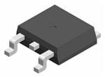
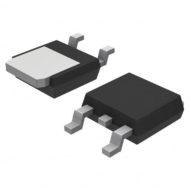
| 供应商器件封装 | DPAK-3 |
| 其它名称 | MC7812CDTRKGOSCT |
| 包装 | 剪切带 (CT) |
| 商标 | ON Semiconductor |
| 安装类型 | 表面贴装 |
| 安装风格 | SMD/SMT |
| 封装 | Reel |
| 封装/外壳 | TO-252-3,DPak(2 引线+接片),SC-63 |
| 封装/箱体 | TO-252-3 (DPAK) |
| 工作温度 | 0°C ~ 125°C |
| 工厂包装数量 | 2500 |
| 最大工作温度 | + 125 C |
| 最大输入电压 | 35 V |
| 最小工作温度 | 0 C |
| 最小输入电压 | 14 V |
| 极性 | Positive |
| 标准包装 | 1 |
| 电压-跌落(典型值) | 2V @ 1A |
| 电压-输入 | 最高 35V |
| 电压-输出 | 12V |
| 电流-输出 | 1A |
| 电流-限制(最小值) | - |
| 稳压器拓扑 | 正,固定式 |
| 稳压器数 | 1 |
| 系列 | MC7812 |
| 线路调整率 | 48 mV |
| 负载调节 | 60 mV |
| 输出电压 | 12 V |
| 输出电流 | 1 A |
| 输出端数量 | 1 |
| 输出类型 | Fixed |


- 商务部:美国ITC正式对集成电路等产品启动337调查
- 曝三星4nm工艺存在良率问题 高通将骁龙8 Gen1或转产台积电
- 太阳诱电将投资9.5亿元在常州建新厂生产MLCC 预计2023年完工
- 英特尔发布欧洲新工厂建设计划 深化IDM 2.0 战略
- 台积电先进制程称霸业界 有大客户加持明年业绩稳了
- 达到5530亿美元!SIA预计今年全球半导体销售额将创下新高
- 英特尔拟将自动驾驶子公司Mobileye上市 估值或超500亿美元
- 三星加码芯片和SET,合并消费电子和移动部门,撤换高东真等 CEO
- 三星电子宣布重大人事变动 还合并消费电子和移动部门
- 海关总署:前11个月进口集成电路产品价值2.52万亿元 增长14.8%


PDF Datasheet 数据手册内容提取
MC7800, MC7800A, MC7800AE, NCV7800 1.0 A Positive Voltage Regulators These voltage regulators are monolithic integrated circuits designed as fixed−voltage regulators for a wide variety of applications http://onsemi.com including local, on−card regulation. These regulators employ internal current limiting, thermal shutdown, and safe−area compensation. With adequate heatsinking they can deliver output currents in excess of TO−220 1.0 A. Although designed primarily as a fixed voltage regulator, these T SUFFIX devices can be used with external components to obtain adjustable CASE 221AB voltages and currents. Heatsink surface 1 connected to Pin 2. Features 2 3 • Output Current in Excess of 1.0 A • No External Components Required Pin 1.Input D2PAK−3 • 2.Ground D2T SUFFIX Internal Thermal Overload Protection 1 3.Output CASE 936 • Internal Short Circuit Current Limiting 3 • Output Transistor Safe−Area Compensation Heatsink surface (shown as terminal 4 in • case outline drawing) is connected to Pin 2. Output Voltage Offered in 1.5%, 2% and 4% Tolerance • Available in Surface Mount D2PAK−3, DPAK−3 and Standard 4 DPAK−3 3−Lead Transistor Packages DT SUFFIX • 1 2 CASE 369C NCV Prefix for Automotive and Other Applications Requiring 3 Unique Site and Control Change Requirements; AEC−Q100 Qualified and PPAP Capable STANDARD APPLICATION • These are Pb−Free Devices Input MC78XX Output MAXIMUM RATINGS (TA = 25°C, unless otherwise noted) 0.33C (cid:3)inF* CO** Value Unit Rating Symbol 369C 221A 936 A common ground is required between the Input Voltage (5.0 − 18 V) VI 35 Vdc input and the output voltages. The input voltage (24 V) 40 must remain typically 2.0 V above the output Power Dissipation PD Internally Limited W voltage even during the low point on the input ripple voltage. Thermal Resistance, R(cid:2)JA 92 65 Figure °C/W Junction−to−Ambient 15 XX, These two digits of the type number indicate nominal voltage. Thermal Resistance, R(cid:2)JC 5.0 5.0 5.0 °C/W Junction−to−Case * Cin is required if regulator is located an appreciable distance from power supply Storage Junction Temperature Tstg −65 to +150 °C filter. Range ** CO is not needed for stability; however, Operating Junction Temperature TJ +150 °C iot fd leosess tihmapnr o0v.1e (cid:3)trFa ncsoieunldt creasupsoen isnes.t aVbailluitye.s Stresses exceeding those listed in the Maximum Ratings table may damage the device. If any of these limits are exceeded, device functionality should not be assumed, damage may occur and reliability may be affected. ORDERING INFORMATION *This device series contains ESD protection and exceeds the following tests: See detailed ordering and shipping information in the package Human Body Model 2000 V per MIL_STD_883, Method 3015. dimensions section on page 23 of this data sheet. Machine Model Method 200 V. DEVICE MARKING INFORMATION See general marking information in the device marking section on page 28 of this data sheet. © Semiconductor Components Industries, LLC, 2014 1 Publication Order Number: November, 2014 − Rev. 27 MC7800/D
MC7800, MC7800A, MC7800AE, NCV7800 Vin MC7800 R24 50 D2 Zener LAT LAT 3 A Q17 Q18 R19 27.5 k Q19 QNPN Q20 QNPN C3 1.0 P R14 1.0 k Q10 QNPN R15 R18 R21 680 R23 100 k R22 600 0.2 100 Vout Q7 5.01 QNPN Q5 QNPN 2 R30 R17 Q12 18 k 9.0 k Q9 QNPN Sense QNPN 2 R12 R29 DZe1ner R1 QQ6NPN R151 1k QNQP1N5 3R.02 5k R9.208 k 10.66 k R16 R10 6.0 k 9.0 k R1725000 600 3340-(3316ACT) R26 R27 Q8 3.0 k 9.0 k QNPN R2 1.56 k R9 R5 3.0 k R13 4.5 k SUB 11660 QNQP1N4 Q1 C1 Q11 2 C2 N+ 30 P 3.0 P QNPN 6 Q4 QNPN Q13 Q3 QNPN Q2 Q16 QNPN R6 QNPN 4 1.0 k Diode R7 R3 R8 14 k 1.8 k 5.0 k This device contains 22 active transistors. Figure 1. Representative Schematic Diagram http://onsemi.com 2
MC7800, MC7800A, MC7800AE, NCV7800 ELECTRICAL CHARACTERISTICS (Vin = 10 V, IO = 500 mA, TJ = Tlow to 125°C (Note 1), unless otherwise noted) MC7805B, NCV7805B MC7805C Characteristic Symbol Min Typ Max Min Typ Max Unit Output Voltage (TJ = 25°C) VO 4.8 5.0 5.2 4.8 5.0 5.2 Vdc Output Voltage (5.0 mA ≤ IO ≤ 1.0 A, PD ≤ 15 W) VO Vdc 7.0 Vdc ≤ Vin ≤ 20 Vdc − − − 4.75 5.0 5.25 8.0 Vdc ≤ Vin ≤ 20 Vdc 4.75 5.0 5.25 − − − Line Regulation (Note 4) Regline mV 7.5 Vdc ≤ Vin ≤ 20 Vdc, 1.0 A − 5.0 100 − 0.5 20 8.0 Vdc ≤ Vin ≤ 12 Vdc − 1.3 50 − 0.8 10 Load Regulation (Note 4) Regload mV 5.0 mA ≤ IO ≤ 1.0 A − 1.3 100 − 1.3 25 5.0 mA ≤ IO ≤ 1.5 A (TA = 25°C) − 0.15 50 − 1.3 25 Quiescent Current IB − 3.2 8.0 − 3.2 6.5 mA Quiescent Current Change (cid:4)IB mA 7.0 Vdc ≤ Vin ≤ 25 Vdc − − − − 0.3 1.0 5.0 mA ≤ IO ≤ 1.0 A (TA = 25°C) − − 0.5 − 0.08 0.8 Ripple Rejection RR dB 8.0 Vdc ≤ Vin ≤ 18 Vdc, f = 120 Hz − 68 − 62 83 − Dropout Voltage (IO = 1.0 A, TJ = 25°C) VI − VO − 2.0 − − 2.0 − Vdc Output Noise Voltage (TA = 25°C) Vn (cid:3)V/VO 10 Hz ≤ f ≤ 100 kHz − 10 − − 10 − Output Resistance f = 1.0 kHz rO − 0.9 − − 0.9 − m(cid:5) Short Circuit Current Limit (TA = 25°C) ISC A Vin = 35 Vdc − 0.2 − − 0.6 − Peak Output Current (TJ = 25°C) Imax − 2.2 − − 2.2 − A Average Temperature Coefficient of Output Voltage TCVO − −0.3 − − −0.3 − mV/°C 1. Tlow = 0°C for MC78XXC, MC78XXAC, = (cid:2)40°C for NCV78XX, MC78XXB, MC78XXAB, and MC78XXAEB 2. Load and line regulation are specified at constant junction temperature. Changes in VO due to heating effects must be taken into account separately. Pulse testing with low duty cycle is used. http://onsemi.com 3
MC7800, MC7800A, MC7800AE, NCV7800 ELECTRICAL CHARACTERISTICS (Vin = 10 V, IO = 1.0 A, TJ = Tlow to 125°C (Note 3), unless otherwise noted) MC7805AB/MC7805AC/NCV7805AB Characteristic Symbol Min Typ Max Unit Output Voltage (TJ = 25°C) VO 4.9 5.0 5.1 Vdc Output Voltage (5.0 mA ≤ IO ≤ 1.0 A, PD ≤ 15 W) VO Vdc 7.5 Vdc ≤ Vin ≤ 20 Vdc 4.8 5.0 5.2 Line Regulation (Note 4) Regline mV 7.5 Vdc ≤ Vin ≤ 25 Vdc, IO = 500 mA − 0.5 10 8.0 Vdc ≤ Vin ≤ 12 Vdc, IO = 1.0 A − 0.8 12 8.0 Vdc ≤ Vin ≤ 12 Vdc, IO = 1.0 A, TJ = 25°C − 1.3 4.0 7.3 Vdc ≤ Vin ≤ 20 Vdc, IO = 1.0 A, TJ = 25°C − 4.5 10 Load Regulation (Note 4) Regload mV 5.0 mA ≤ IO ≤ 1.5 A, TJ = 25°C − 1.3 25 5.0 mA ≤ IO ≤ 1.0 A − 0.8 25 250 mA ≤ IO ≤ 750 mA − 0.53 15 Quiescent Current IB − 3.2 6.0 mA Quiescent Current Change (cid:4)IB mA 8.0 Vdc ≤ Vin ≤ 25 Vdc, IO = 500 mA − 0.3 0.8 7.5 Vdc ≤ Vin ≤ 20 Vdc, TJ = 25°C − − 0.8 5.0 mA ≤ IO ≤ 1.0 A − 0.08 0.5 Ripple Rejection RR dB 8.0 Vdc ≤ Vin ≤ 18 Vdc, f = 120 Hz, IO = 500 mA 68 83 − Dropout Voltage (IO = 1.0 A, TJ = 25°C) VI − VO − 2.0 − Vdc Output Noise Voltage (TA = 25°C) Vn (cid:3)V/VO 10 Hz ≤ f ≤ 100 kHz − 10 − Output Resistance (f = 1.0 kHz) rO − 0.9 − m(cid:5) Short Circuit Current Limit (TA = 25°C) ISC A Vin = 35 Vdc − 0.2 − Peak Output Current (TJ = 25°C) Imax − 2.2 − A Average Temperature Coefficient of Output Voltage TCVO − −0.3 − mV/°C 3. Tlow = 0°C for MC78XXC, MC78XXAC, = (cid:2)40°C for NCV78XX, MC78XXB, MC78XXAB, and MC78XXAEB 4. Load and line regulation are specified at constant junction temperature. Changes in VO due to heating effects must be taken into account separately. Pulse testing with low duty cycle is used. http://onsemi.com 4
MC7800, MC7800A, MC7800AE, NCV7800 ELECTRICAL CHARACTERISTICS (Vin = 11 V, IO = 500 mA, TJ = Tlow to 125°C (Note 5), unless otherwise noted) MC7806B/NCV7806B MC7806C Characteristic Symbol Min Typ Max Min Typ Max Unit Output Voltage (TJ = 25°C) VO 5.75 6.0 6.25 5.75 6.0 6.25 Vdc Output Voltage (5.0 mA ≤ IO ≤ 1.0 A, PD ≤ 15 W) VO Vdc 8.0 Vdc ≤ Vin ≤ 21 Vdc − − − 5.7 6.0 6.3 9.0 Vdc ≤ Vin ≤ 21 Vdc 5.7 6.0 6.3 − − − Line Regulation, TJ = 25°C (Note 6) Regline mV 8.0 Vdc ≤ Vin ≤ 25 Vdc − 5.5 120 − 0.5 24 9.0 Vdc ≤ Vin ≤ 13 Vdc − 1.4 60 − 0.8 12 Load Regulation, TJ = 25°C (Note 6) Regload mV 5.0 mA ≤ IO ≤ 1.5 A − 1.3 120 − 1.3 30 Quiescent Current (TJ = 25°C) IB − 3.3 8.0 − 3.3 8.0 mA Quiescent Current Change (cid:4)IB mA 8.0 Vdc ≤ Vin ≤ 25 Vdc − − − − 0.3 1.3 5.0 mA ≤ IO ≤ 1.0 A − − 0.5 − 0.08 0.5 Ripple Rejection RR dB 9.0 Vdc ≤ Vin ≤ 19 Vdc, f = 120 Hz − 65 − 58 65 − Dropout Voltage (IO = 1.0 A, TJ = 25°C) VI − VO − 2.0 − − 2.0 − Vdc Output Noise Voltage (TA = 25°C) Vn (cid:3)V/VO 10 Hz ≤ f ≤ 100 kHz − 10 − − 10 − Output Resistance f = 1.0 kHz rO − 0.9 − − 0.9 − m(cid:5) Short Circuit Current Limit (TA = 25°C) ISC A Vin = 35 Vdc − 0.2 − − 0.2 − Peak Output Current (TJ = 25°C) Imax − 2.2 − − 2.2 − A Average Temperature Coefficient of Output Voltage TCVO − −0.3 − − −0.3 − mV/°C 5. Tlow = 0°C for MC78XXC, MC78XXAC, = (cid:2)40°C for NCV78XX, MC78XXB, MC78XXAB, and MC78XXAEB 6. Load and line regulation are specified at constant junction temperature. Changes in VO due to heating effects must be taken into account separately. Pulse testing with low duty cycle is used. http://onsemi.com 5
MC7800, MC7800A, MC7800AE, NCV7800 ELECTRICAL CHARACTERISTICS (Vin = 11 V, IO = 1.0 A, TJ = Tlow to 125°C (Note 7), unless otherwise noted) MC7806AC Characteristic Symbol Min Typ Max Unit Output Voltage (TJ = 25°C) VO 5.88 6.0 6.12 Vdc Output Voltage (5.0 mA ≤ IO ≤ 1.0 A, PD ≤ 15 W) VO Vdc 8.6 Vdc ≤ Vin ≤ 21 Vdc 5.76 6.0 6.24 Line Regulation (Note 8) Regline mV 8.6 Vdc ≤ Vin ≤ 25 Vdc, IO = 500 mA − 5.0 12 9.0 Vdc ≤ Vin ≤ 13 Vdc, IO = 1.0 A − 1.4 15 Load Regulation (Note 8) Regload mV 5.0 mA ≤ IO ≤ 1.5 A, TJ = 25°C − 1.3 25 5.0 mA ≤ IO ≤ 1.0 A − 0.9 25 250 mA ≤ IO ≤ 750 mA − 0.2 15 Quiescent Current IB − 3.3 6.0 mA Quiescent Current Change (cid:4)IB mA 9.0 Vdc ≤ Vin ≤ 25 Vdc, IO = 500 mA − − 0.8 9.0 Vdc ≤ Vin ≤ 21 Vdc, IO = 1.0 A, TJ = 25°C − − 0.8 5.0 mA ≤ IO ≤ 1.0 A − − 0.5 Ripple Rejection RR dB 9.0 Vdc ≤ Vin ≤ 19 Vdc, f = 120 Hz, IO = 500 mA 58 65 − Dropout Voltage (IO = 1.0 A, TJ = 25°C) VI − VO − 2.0 − Vdc Output Noise Voltage (TA = 25°C) Vn (cid:3)V/VO 10 Hz ≤ f ≤ 100 kHz − 10 − Output Resistance (f = 1.0 kHz) rO − 0.9 − m(cid:5) Short Circuit Current Limit (TA = 25°C) ISC A Vin = 35 Vdc − 0.2 − Peak Output Current (TJ = 25°C) Imax − 2.2 − A Average Temperature Coefficient of Output Voltage TCVO − −0.3 − mV/°C 7. Tlow = 0°C for MC78XXC, MC78XXAC, = (cid:2)40°C for NCV78XX, MC78XXB, MC78XXAB, and MC78XXAEB 8. Load and line regulation are specified at constant junction temperature. Changes in VO due to heating effects must be taken into account separately. Pulse testing with low duty cycle is used. http://onsemi.com 6
MC7800, MC7800A, MC7800AE, NCV7800 ELECTRICAL CHARACTERISTICS (Vin = 14 V, IO = 500 mA, TJ = Tlow to 125°C (Note 9), unless otherwise noted) MC7808B/NCV7808B MC7808C Characteristic Symbol Min Typ Max Min Typ Max Unit Output Voltage (TJ = 25°C) VO 7.7 8.0 8.3 7.7 8.0 8.3 Vdc Output Voltage (5.0 mA ≤ IO ≤ 1.0 A, PD ≤ 15 W) VO Vdc 10.5 Vdc ≤ Vin ≤ 23 Vdc − − − 7.6 8.0 8.4 11.5 Vdc ≤ Vin ≤ 23 Vdc 7.6 8.0 8.4 − − − Line Regulation, TJ = 25°C, (Note 10) Regline mV 10.5 Vdc ≤ Vin ≤ 25 Vdc − 6.0 160 − 6.0 32 11 Vdc ≤ Vin ≤ 17 Vdc − 1.7 80 − 1.7 16 Load Regulation, TJ = 25°C (Note 10) Regload mV 5.0 mA ≤ IO ≤ 1.5 A − 1.4 160 − 1.4 35 Quiescent Current IB − 3.3 8.0 − 3.3 8.0 mA Quiescent Current Change (cid:4)IB mA 10.5 Vdc ≤ Vin ≤ 25 Vdc − − − − − 1.0 5.0 mA ≤ IO ≤ 1.0 A − − 0.5 − − 0.5 Ripple Rejection RR dB 11.5 Vdc ≤ Vin ≤ 18 Vdc, f = 120 Hz − 62 − 56 62 − Dropout Voltage (IO = 1.0 A, TJ = 25°C) VI − VO − 2.0 − − 2.0 − Vdc Output Noise Voltage (TA = 25°C) Vn (cid:3)V/VO 10 Hz ≤ f ≤ 100 kHz − 10 − − 10 − Output Resistance f = 1.0 kHz rO − 0.9 − − 0.9 − m(cid:5) Short Circuit Current Limit (TA = 25°C) ISC A Vin = 35 Vdc − 0.2 − − 0.2 − Peak Output Current (TJ = 25°C) Imax − 2.2 − − 2.2 − A Average Temperature Coefficient of Output Voltage TCVO − −0.4 − − −0.4 − mV/°C 9. Tlow = 0°C for MC78XXC, MC78XXAC, = (cid:2)40°C for NCV78XX, MC78XXB, MC78XXAB, and MC78XXAEB 10.Load and line regulation are specified at constant junction temperature. Changes in VO due to heating effects must be taken into account separately. Pulse testing with low duty cycle is used. http://onsemi.com 7
MC7800, MC7800A, MC7800AE, NCV7800 ELECTRICAL CHARACTERISTICS (Vin = 14 V, IO = 1.0 A, TJ = Tlow to 125°C (Note 11), unless otherwise noted) MC7808AB/MC7808AC/NCV7808AB Characteristic Symbol Min Typ Max Unit Output Voltage (TJ = 25°C) VO 7.84 8.0 8.16 Vdc Output Voltage (5.0 mA ≤ IO ≤ 1.0 A, PD ≤ 15 W) VO Vdc 10.6 Vdc ≤ Vin ≤ 23 Vdc 7.7 8.0 8.3 Line Regulation (Note 12) Regline mV 10.6 Vdc ≤ Vin ≤ 25 Vdc, IO = 500 mA − 6.0 15 11 Vdc ≤ Vin ≤ 17 Vdc, IO = 1.0 A − 1.7 18 10.4 Vdc ≤ Vin ≤ 23 Vdc, TJ = 25°C − 5.0 15 Load Regulation (Note 12) Regload mV 5.0 mA ≤ IO ≤ 1.5 A, TJ = 25°C − 1.4 25 5.0 mA ≤ IO ≤ 1.0 A − 1.0 25 250 mA ≤ IO ≤ 750 mA − 0.22 15 Quiescent Current IB − 3.3 6.0 mA Quiescent Current Change (cid:4)IB mA 11 Vdc ≤ Vin ≤ 25 Vdc, IO = 500 mA − − 0.8 10.6 Vdc ≤ Vin ≤ 23 Vdc, IO = 1.0 A, TJ = 25°C − − 0.8 5.0 mA ≤ IO ≤ 1.0 A − − 0.5 Ripple Rejection RR dB 11.5 Vdc ≤ Vin ≤ 21.5 Vdc, f = 120 Hz, IO = 500 mA 56 62 − Dropout Voltage (IO = 1.0 A, TJ = 25°C) VI − VO − 2.0 − Vdc Output Noise Voltage (TA = 25°C) Vn (cid:3)V/VO 10 Hz ≤ f ≤ 100 kHz − 10 − Output Resistance f = 1.0 kHz rO − 0.9 − m(cid:5) Short Circuit Current Limit (TA = 25°C) ISC A Vin = 35 Vdc − 0.2 − Peak Output Current (TJ = 25°C) Imax − 2.2 − A Average Temperature Coefficient of Output Voltage TCVO − −0.4 − mV/°C 11.Tlow = 0°C for MC78XXC, MC78XXAC, = (cid:2)40°C for NCV78XX, MC78XXB, MC78XXAB, and MC78XXAEB 12.Load and line regulation are specified at constant junction temperature. Changes in VO due to heating effects must be taken into account separately. Pulse testing with low duty cycle is used. http://onsemi.com 8
MC7800, MC7800A, MC7800AE, NCV7800 ELECTRICAL CHARACTERISTICS (Vin = 15 V, IO = 500 mA, TJ = Tlow to 125°C (Note 13), unless otherwise noted) MC7809B/NCV7809B MC7809C Characteristic Symbol Min Typ Max Min Typ Max Unit Output Voltage (TJ = 25°C) VO 8.65 9.0 9.35 8.65 9.0 9.35 Vdc Output Voltage (5.0 mA ≤ IO ≤ 1.0 A, PD ≤ 15 W) VO Vdc 11.5 Vdc ≤ Vin ≤ 24 Vdc 8.55 9.0 9.45 8.55 9.0 9.45 Line Regulation, TJ = 25°C (Note 14) Regline mV 11 Vdc ≤ Vin ≤ 26 Vdc − 6.2 32 − 6.2 32 11.5 Vdc ≤ Vin ≤ 17 Vdc − 1.8 16 − 1.8 16 Load Regulation, TJ = 25°C (Note 14) Regload mV 5.0 mA ≤ IO ≤ 1.5 A − 1.5 35 − 1.5 35 Quiescent Current IB − 3.4 8.0 − 3.4 8.0 mA Quiescent Current Change (cid:4)IB mA 11.5 Vdc ≤ Vin ≤ 26 Vdc − − 1.0 − − 1.0 5.0 mA ≤ IO ≤ 1.0 A − − 0.5 − − 0.5 Ripple Rejection RR dB 11.5 Vdc ≤ Vin ≤ 21.5 Vdc, f = 120 Hz 56 61 − 56 61 − Dropout Voltage (IO = 1.0 A, TJ = 25°C) VI − VO − 2.0 − − 2.0 − Vdc Output Noise Voltage (TA = 25°C) Vn (cid:3)V/VO 10 Hz ≤ f ≤ 100 kHz − 10 − − 10 − Output Resistance f = 1.0 kHz rO − 1.0 − − 1.0 − m(cid:5) Short Circuit Current Limit (TA = 25°C) ISC A Vin = 35 Vdc − 0.2 − − 0.2 − Peak Output Current (TJ = 25°C) Imax − 2.2 − − 2.2 − A Average Temperature Coefficient of Output Voltage TCVO − −0.5 − − −0.5 − mV/°C 13.Tlow = 0°C for MC78XXC, MC78XXAC, = (cid:2)40°C for NCV78XX, MC78XXB, MC78XXAB, and MC78XXAEB 14.Load and line regulation are specified at constant junction temperature. Changes in VO due to heating effects must be taken into account separately. Pulse testing with low duty cycle is used. http://onsemi.com 9
MC7800, MC7800A, MC7800AE, NCV7800 ELECTRICAL CHARACTERISTICS (Vin = 15 V, IO = 1.0 A, TJ = Tlow to 125°C (Note 15), unless otherwise noted) MC7809AB/MC7809AC Characteristic Symbol Min Typ Max Unit Output Voltage (TJ = 25°C) VO 8.82 9.0 9.18 Vdc Output Voltage (5.0 mA ≤ IO ≤ 1.0 A, PD ≤ 15 W) VO Vdc 11.5 Vdc ≤ Vin ≤ 24 Vdc 8.65 9.0 9.35 Line Regulation (Note 16) Regline mV 11.5 Vdc ≤ Vin ≤ 26 Vdc, IO = 500 mA − 6.2 16 12 Vdc ≤ Vin ≤ 17 Vdc, IO = 1.0 A − 1.8 7.0 11.5 Vdc ≤ Vin ≤ 24 Vdc, TJ = 25°C − 5.2 16 Load Regulation (Note 16) Regload mV 5.0 mA ≤ IO ≤ 1.5 A, TJ = 25°C − − 25 5.0 mA ≤ IO ≤ 1.0 A − − 25 250 mA ≤ IO ≤ 750 mA − − 15 Quiescent Current IB − 3.3 6.0 mA Quiescent Current Change (cid:4)IB mA 11.5 Vdc ≤ Vin ≤ 26 Vdc, IO = 500 mA − − 0.8 11.5 Vdc ≤ Vin ≤ 24 Vdc, IO = 1.0 A, TJ = 25°C − − 0.8 5.0 mA ≤ IO ≤ 1.0 A − − 0.5 Ripple Rejection RR dB 11.5 Vdc ≤ Vin ≤ 21.5 Vdc, f = 120 Hz, IO = 500 mA 56 61 − Dropout Voltage (IO = 1.0 A, TJ = 25°C) VI _ VO 2.0 Vdc Output Noise Voltage (TA = 25°C) Vn (cid:3)V/VO 10 Hz ≤ f ≤ 100 kHz − 10 − Output Resistance f = 1.0 kHz rO − 1.0 − m(cid:5) Short Circuit Current Limit (TA = 25°C) ISC A Vin = 35 Vdc − 0.2 − Peak Output Current (TJ = 25°C) Imax − 2.2 − A Average Temperature Coefficient of Output Voltage TCVO − −0.5 − mV/°C 15.Tlow = 0°C for MC78XXC, MC78XXAC, = (cid:2)40°C for NCV78XX, MC78XXB, MC78XXAB. 16.Load and line regulation are specified at constant junction temperature. Changes in VO due to heating effects must be taken into account separately. Pulse testing with low duty cycle is used. http://onsemi.com 10
MC7800, MC7800A, MC7800AE, NCV7800 ELECTRICAL CHARACTERISTICS (Vin = 19 V, IO = 500 mA, TJ = Tlow to 125°C (Note 17), unless otherwise noted) MC7812B/NCV7812B MC7812C Characteristic Symbol Min Typ Max Min Typ Max Unit Output Voltage (TJ = 25°C) VO 11.5 12 12.5 11.5 12 12.5 Vdc Output Voltage (5.0 mA ≤ IO ≤ 1.0 A, PD ≤ 15 W) VO Vdc 14.5 Vdc ≤ Vin ≤ 27 Vdc − − − 11.4 12 12.6 15.5 Vdc ≤ Vin ≤ 27 Vdc 11.4 12 12.6 − − − Line Regulation, TJ = 25°C (Note 18) Regline mV 14.5 Vdc ≤ Vin ≤ 30 Vdc − 7.5 240 − 3.8 24 16 Vdc ≤ Vin ≤ 22 Vdc − 2.2 120 − 0.3 24 14.8 Vdc ≤ Vin ≤ 27 Vdc, IO = 1.0 A − − − − − 48 Load Regulation, TJ = 25°C (Note 18) Regload mV 5.0 mA ≤ IO ≤ 1.5 A − 1.6 240 − 8.1 60 Quiescent Current IB − 3.4 8.0 − 3.4 6.5 mA Quiescent Current Change (cid:4)IB mA 14.5 Vdc ≤ Vin ≤ 30 Vdc, IO = 1.0 A, TJ = 25°C − − − − − 0.7 15 Vdc ≤ Vin ≤ 30 Vdc − − 1.0 − − 0.8 5.0 mA ≤ IO ≤ 1.0 A − − 0.5 − − 0.5 Ripple Rejection RR dB 15 Vdc ≤ Vin ≤ 25 Vdc, f = 120 Hz − 60 − 55 60 − Dropout Voltage (IO = 1.0 A, TJ = 25°C) VI − VO − 2.0 − − 2.0 − Vdc Output Noise Voltage (TA = 25°C) Vn (cid:3)V/VO 10 Hz ≤ f ≤ 100 kHz − 10 − − 10 − Output Resistance f = 1.0 kHz rO − 1.1 − − 1.1 − m(cid:5) Short Circuit Current Limit (TA = 25°C) ISC A Vin = 35 Vdc − 0.2 − − 0.2 − Peak Output Current (TJ = 25°C) Imax − 2.2 − − 2.2 − A Average Temperature Coefficient of Output Voltage TCVO − −0.8 − − −0.8 − mV/°C 17.Tlow = 0°C for MC78XXC, MC78XXAC, = (cid:2)40°C for NCV78XX, MC78XXB, MC78XXAB, and MC78XXAEB 18.Load and line regulation are specified at constant junction temperature. Changes in VO due to heating effects must be taken into account separately. Pulse testing with low duty cycle is used. http://onsemi.com 11
MC7800, MC7800A, MC7800AE, NCV7800 ELECTRICAL CHARACTERISTICS (Vin = 19 V, IO = 1.0 A, TJ = Tlow to 125°C (Note 19), unless otherwise noted) MC7812AB/MC7812AC/NCV7812AB Characteristic Symbol Min Typ Max Unit Output Voltage (TJ = 25°C) VO 11.75 12 12.25 Vdc Output Voltage (5.0 mA ≤ IO ≤ 1.0 A, PD ≤ 15 W) VO Vdc 14.8 Vdc ≤ Vin ≤ 27 Vdc 11.5 12 12.5 Line Regulation (Note 20) Regline mV 14.8 Vdc ≤ Vin ≤ 30 Vdc, IO = 500 mA − 3.8 18 16 Vdc ≤ Vin ≤ 22 Vdc, IO = 1.0 A − 2.2 20 14.5 Vdc ≤ Vin ≤ 27 Vdc, TJ = 25°C − 6.0 120 Load Regulation (Note 20) Regload mV 5.0 mA ≤ IO ≤ 1.5 A, TJ = 25°C − − 25 5.0 mA ≤ IO ≤ 1.0 A − − 25 Quiescent Current IB − 3.4 6.0 mA Quiescent Current Change (cid:4)IB mA 15 Vdc ≤ Vin ≤ 30 Vdc, IO = 500 mA − − 0.8 14.8 Vdc ≤ Vin ≤ 27 Vdc, TJ = 25°C − − 0.8 5.0 mA ≤ IO ≤ 1.0 A, TJ = 25°C − − 0.5 Ripple Rejection RR dB 15 Vdc ≤ Vin ≤ 25 Vdc, f = 120 Hz, IO = 500 mA 55 60 − Dropout Voltage (IO = 1.0 A, TJ = 25°C) VI − VO − 2.0 − Vdc Output Noise Voltage (TA = 25°C) Vn (cid:3)V/VO 10 Hz ≤ f ≤ 100 kHz − 10 − Output Resistance (f = 1.0 kHz) rO − 1.1 − m(cid:5) Short Circuit Current Limit (TA = 25°C) ISC A Vin = 35 Vdc − 0.2 − Peak Output Current (TJ = 25°C) Imax − 2.2 − A Average Temperature Coefficient of Output Voltage TCVO − −0.8 − mV/°C 19.Tlow = 0°C for MC78XXC, MC78XXAC, = (cid:2)40°C for NCV78XX, MC78XXB, MC78XXAB, and MC78XXAEB 20.Load and line regulation are specified at constant junction temperature. Changes in VO due to heating effects must be taken into account separately. Pulse testing with low duty cycle is used. http://onsemi.com 12
MC7800, MC7800A, MC7800AE, NCV7800 ELECTRICAL CHARACTERISTICS (Vin = 23 V, IO = 500 mA, TJ = Tlow to 125°C (Note 21), unless otherwise noted) MC7815B/NCV7815B MC7815C Characteristic Symbol Min Typ Max Min Typ Max Unit Output Voltage (TJ = 25°C) VO 14.4 15 15.6 14.4 15 15.6 Vdc Output Voltage (5.0 mA ≤ IO ≤ 1.0 A, PD ≤ 15 W) VO Vdc 17.5 Vdc ≤ Vin ≤ 30 Vdc − − − 14.25 15 15.75 18.5 Vdc ≤ Vin ≤ 30 Vdc 14.25 15 15.75 − − − Line Regulation, TJ = 25°C (Note 22) Regline mV 17.9 Vdc ≤ Vin ≤ 30 Vdc − 8.5 300 − 8.5 30 20 Vdc ≤ Vin ≤ 26 Vdc − 3.0 150 − 3.0 28 Load Regulation, TJ = 25°C (Note 22) Regload mV 5.0 mA ≤ IO ≤ 1.5 A − 1.8 300 − 1.8 55 Quiescent Current IB − 3.5 8.0 − 3.5 6.5 mA Quiescent Current Change (cid:4)IB mA 17.5 Vdc ≤ Vin ≤ 30 Vdc − − − − − 0.8 17.5 Vdc ≤ Vin ≤ 30 Vdc, IO = 1.0 A, TJ = 25°C − − 1.0 − − 0.7 5.0 mA ≤ IO ≤ 1.0 A − − 0.5 − − 0.5 Ripple Rejection RR dB 18.5 Vdc ≤ Vin ≤ 28.5 Vdc, f = 120 Hz − 58 − 54 58 − Dropout Voltage (IO = 1.0 A, TJ = 25°C) VI − VO − 2.0 − − 2.0 − Vdc Output Noise Voltage (TA = 25°C) Vn (cid:3)V/VO 10 Hz ≤ f ≤ 100 kHz − 10 − − 10 − Output Resistance f = 1.0 kHz rO − 1.2 − − 1.2 − m(cid:5) Short Circuit Current Limit (TA = 25°C) ISC A Vin = 35 Vdc − 0.2 − − 0.2 − Peak Output Current (TJ = 25°C) Imax − 2.2 − − 2.2 − A Average Temperature Coefficient of Output Voltage TCVO − −1.0 − − −1.0 − mV/°C 21.Tlow = 0°C for MC78XXC, MC78XXAC, = (cid:2)40°C for NCV78XX, MC78XXB, MC78XXAB, and MC78XXAEB 22.Load and line regulation are specified at constant junction temperature. Changes in VO due to heating effects must be taken into account separately. Pulse testing with low duty cycle is used. http://onsemi.com 13
MC7800, MC7800A, MC7800AE, NCV7800 ELECTRICAL CHARACTERISTICS (Vin = 23 V, IO = 1.0 A, TJ = Tlow to 125°C (Note 23), unless otherwise noted) MC7815AB/MC7815AC Characteristic Symbol Min Typ Max Unit Output Voltage (TJ = 25°C) VO 14.7 15 15.3 Vdc Output Voltage (5.0 mA ≤ IO ≤ 1.0 A, PD ≤ 15 W) VO Vdc 17.9 Vdc ≤ Vin ≤ 30 Vdc 14.4 15 15.6 Line Regulation (Note 24) Regline mV 17.9 Vdc ≤ Vin ≤ 30 Vdc, IO = 500 mA − 8.5 20 20 Vdc ≤ Vin ≤ 26 Vdc − 3.0 22 17.5 Vdc ≤ Vin ≤ 30 Vdc, IO = 1.0 A, TJ = 25°C − 7.0 20 Load Regulation (Note 24) Regload mV 5.0 mA ≤ IO ≤ 1.5 A, TJ = 25°C − 1.8 25 5.0 mA ≤ IO ≤ 1.0 A − 1.5 25 250 mA ≤ IO ≤ 750 mA − 1.2 15 Quiescent Current IB − 3.5 6.0 mA Quiescent Current Change (cid:4)IB mA 17.5 Vdc ≤ Vin ≤ 30 Vdc, IO = 500 mA − − 0.8 17.5 Vdc ≤ Vin ≤ 30 Vdc, IO = 1.0 A, TJ = 25°C − − 0.8 5.0 mA ≤ IO ≤ 1.0 A − − 0.5 Ripple Rejection RR dB 18.5 Vdc ≤ Vin ≤ 28.5 Vdc, f = 120 Hz, IO = 500 mA 60 80 − Dropout Voltage (IO = 1.0 A, TJ = 25°C) VI − VO − 2.0 − Vdc Output Noise Voltage (TA = 25°C) Vn (cid:3)V/VO 10 Hz ≤ f ≤ 100 kHz − 10 − Output Resistance f = 1.0 kHz rO − 1.2 − m(cid:5) Short Circuit Current Limit (TA = 25°C) ISC A Vin = 35 Vdc − 0.2 − Peak Output Current (TJ = 25°C) Imax − 2.2 − A Average Temperature Coefficient of Output Voltage TCVO − −1.0 − mV/°C 23.Tlow = 0°C for MC78XXC, MC78XXAC, = (cid:2)40°C for NCV78XX, MC78XXB, MC78XXAB, and MC78XXAEB 24.Load and line regulation are specified at constant junction temperature. Changes in VO due to heating effects must be taken into account separately. Pulse testing with low duty cycle is used. http://onsemi.com 14
MC7800, MC7800A, MC7800AE, NCV7800 ELECTRICAL CHARACTERISTICS (Vin = 27 V, IO = 500 mA, TJ = Tlow to 125°C (Note 25), unless otherwise noted) MC7818B MC7818C Characteristic Symbol Min Typ Max Min Typ Max Unit Output Voltage (TJ = 25°C) VO 17.3 18 18.7 17.3 18 18.7 Vdc Output Voltage (5.0 mA ≤ IO ≤ 1.0 A, PD ≤ 15 W) VO Vdc 21 Vdc ≤ Vin ≤ 33 Vdc − − − 17.1 18 18.9 22 Vdc ≤ Vin ≤ 33 Vdc 17.1 18 18.9 − − − Line Regulation, (Note 26) Regline mV 21 Vdc ≤ Vin ≤ 33 Vdc − 9.5 360 − 9.5 50 24 Vdc ≤ Vin ≤ 30 Vdc − 3.2 180 − 3.2 25 Load Regulation, (Note 26) Regload mV 5.0 mA ≤ IO ≤ 1.5 A − 2.0 360 − 2.0 55 Quiescent Current IB − 3.5 8.0 − 3.5 6.5 mA Quiescent Current Change (cid:4)IB mA 21 Vdc ≤ Vin ≤ 33 Vdc − − − − − 1.0 5.0 mA ≤ IO ≤ 1.0 A − − 0.5 − − 0.5 Ripple Rejection RR dB 22 Vdc ≤ Vin ≤ 33 Vdc, f = 120 Hz − 57 − 53 57 − Dropout Voltage (IO = 1.0 A, TJ = 25°C) ViI − VO − 2.0 − − 2.0 − Vdc Output Noise Voltage (TA = 25°C) Vn (cid:3)V/VO 10 Hz ≤ f ≤ 100 kHz − 10 − − 10 − Output Resistance f = 1.0 kHz rO − 1.3 − − 1.3 − m(cid:5) Short Circuit Current Limit (TA = 25°C) ISC A Vin = 35 Vdc − 0.2 − − 0.2 − Peak Output Current (TJ = 25°C) Imax − 2.2 − − 2.2 − A Average Temperature Coefficient of Output Voltage TCVO − −1.5 − − −1.5 − mV/°C 25.Tlow = 0°C for MC78XXC, MC78XXAC, = (cid:2)40°C for NCV78XX, MC78XXB, MC78XXAB, and MC78XXAEB 26.Load and line regulation are specified at constant junction temperature. Changes in VO due to heating effects must be taken into account separately. Pulse testing with low duty cycle is used. http://onsemi.com 15
MC7800, MC7800A, MC7800AE, NCV7800 ELECTRICAL CHARACTERISTICS (Vin = 27 V, IO = 1.0 A, TJ = Tlow to 125°C (Note 27), unless otherwise noted) MC7818AC Characteristic Symbol Min Typ Max Unit Output Voltage (TJ = 25°C) VO 17.64 18 18.36 Vdc Output Voltage (5.0 mA ≤ IO ≤ 1.0 A, PD ≤ 15 W) VO Vdc 21 Vdc ≤ Vin ≤ 33 Vdc 17.3 18 18.7 Line Regulation (Note 28) Regline mV 21 Vdc ≤ Vin ≤ 33 Vdc, IO = 500 mA − 9.5 22 24 Vdc ≤ Vin ≤ 30 Vdc, IO = 1.0 A − 3.2 25 24 Vdc ≤ Vin ≤ 30 Vdc, IO = 1.0 A, TJ = 25°C − 3.2 10.5 20.6 Vdc ≤ Vin ≤ 33 Vdc, IO = 1.0 A, TJ = 25°C − 8.0 22 Load Regulation (Note 28) Regload mV 5.0 mA ≤ IO ≤ 1.5 A, TJ = 25°C − 2.0 25 5.0 mA ≤ IO ≤ 1.0 A − 1.8 25 250 mA ≤ IO ≤ 750 mA − 1.5 15 Quiescent Current IB − 3.5 6.0 mA Quiescent Current Change (cid:4)IB mA 21 Vdc ≤ Vin ≤ 33 Vdc, IO = 500 mA − − 0.8 21.5 Vdc ≤ Vin ≤ 30 Vdc, TJ = 25°C − − 0.8 5.0 mA ≤ IO ≤ 1.0 A − − 0.5 Ripple Rejection RR dB 22 Vdc ≤ Vin ≤ 32 Vdc, f = 120 Hz, IO = 500 mA 53 57 − Dropout Voltage (IO = 1.0 A, TJ = 25°C) VI − VO − 2.0 − Vdc Output Noise Voltage (TA = 25°C) Vn (cid:3)V/VO 10 Hz ≤ f ≤ 100 kHz − 10 − Output Resistance f = 1.0 kHz rO − 1.3 − m(cid:5) Short Circuit Current Limit (TA = 25°C) ISC A Vin = 35 Vdc − 0.2 − Peak Output Current (TJ = 25°C) Imax − 2.2 − A Average Temperature Coefficient of Output Voltage TCVO − −1.5 − mV/°C 27.Tlow = 0°C for MC78XXC, MC78XXAC, = (cid:2)40°C for NCV78XX, MC78XXB, MC78XXAB, and MC78XXAEB 28.Load and line regulation are specified at constant junction temperature. Changes in VO due to heating effects must be taken into account separately. Pulse testing with low duty cycle is used. http://onsemi.com 16
MC7800, MC7800A, MC7800AE, NCV7800 ELECTRICAL CHARACTERISTICS (Vin = 33 V, IO = 500 mA, TJ = Tlow to 125°C (Note 29), unless otherwise noted) MC7824B MC7824C Characteristic Symbol Min Typ Max Min Typ Max Unit Output Voltage (TJ = 25°C) VO 23 24 25 23 24 25 Vdc Output Voltage (5.0 mA ≤ IO ≤ 1.0 A, PD ≤ 15 W) VO Vdc 27 Vdc ≤ Vin ≤ 38 Vdc − − − 22.8 24 25.2 28 Vdc ≤ Vin ≤ 38 Vdc 22.8 24 25.2 − − − Line Regulation, (Note 30) Regline mV 27 Vdc ≤ Vin ≤ 38 Vdc − 11.5 480 − 2.7 60 30 Vdc ≤ Vin ≤ 36 Vdc − 3.8 240 − 2.7 48 Load Regulation, (Note 30) Regload mV 5.0 mA ≤ IO ≤ 1.5 A − 2.1 480 − 4.4 65 Quiescent Current IB − 3.6 8.0 − 3.6 6.5 mA Quiescent Current Change (cid:4)IB mA 27 Vdc ≤ Vin ≤ 38 Vdc − − − − − 1.0 5.0 mA ≤ IO ≤ 1.0 A − − 0.5 − − 0.5 Ripple Rejection RR dB 28 Vdc ≤ Vin ≤ 38 Vdc, f = 120 Hz − 54 − 50 54 − Dropout Voltage (IO = 1.0 A, TJ = 25°C) VI − VO − 2.0 − − 2.0 − Vdc Output Noise Voltage (TA = 25°C) Vn (cid:3)V/VO 10 Hz ≤ f ≤ 100 kHz − 10 − − 10 − Output Resistance f = 1.0 kHz rO − 1.4 − − 1.4 − m(cid:5) Short Circuit Current Limit (TA = 25°C) ISC A Vin = 35 Vdc − 0.2 − − 0.2 − Peak Output Current (TJ = 25°C) Imax − 2.2 − − 2.2 − A Average Temperature Coefficient of Output Voltage TCVO − −2.0 − − −2.0 − mV/°C 29.Tlow = 0°C for MC78XXC, MC78XXAC, = (cid:2)40°C for NCV78XX, MC78XXB, MC78XXAB, and MC78XXAEB 30.Load and line regulation are specified at constant junction temperature. Changes in VO due to heating effects must be taken into account separately. Pulse testing with low duty cycle is used. http://onsemi.com 17
MC7800, MC7800A, MC7800AE, NCV7800 ELECTRICAL CHARACTERISTICS (Vin = 33 V, IO = 1.0 A, TJ = Tlow to 125°C (Note 31), unless otherwise noted) MC7824AC Characteristic Symbol Min Typ Max Unit Output Voltage (TJ = 25°C) VO 23.5 24 24.5 Vdc Output Voltage (5.0 mA ≤ IO ≤ 1.0 A, PD ≤ 15 W) VO Vdc 27.3 Vdc ≤ Vin ≤ 38 Vdc 23.2 24 25.8 Line Regulation (Note 32) Regline mV 27 Vdc ≤ Vin ≤ 38 Vdc, IO = 500 mA − 11.5 25 30 Vdc ≤ Vin ≤ 36 Vdc, IO = 1.0 A − 3.8 28 30 Vdc ≤ Vin ≤ 36 Vdc, TJ = 25°C − 3.8 12 26.7 Vdc ≤ Vin ≤ 38 Vdc, IO = 1.0 A, TJ = 25°C − 10 25 Load Regulation (Note 32) Regload mV 5.0 mA ≤ IO ≤ 1.5 A, TJ = 25°C − 2.1 15 5.0 mA ≤ IO ≤ 1.0 A − 2.0 25 250 mA ≤ IO ≤ 750 mA − 1.8 15 Quiescent Current IB − 3.6 6.0 mA Quiescent Current Change (cid:4)IB mA 27.3 Vdc ≤ Vin ≤ 38 Vdc, IO = 500 mA − − 0.8 27 Vdc ≤ Vin ≤ 38 Vdc, TJ = 25°C − − 0.8 5.0 mA ≤ IO ≤ 1.0 A − − 0.5 Ripple Rejection RR dB 28 Vdc ≤ Vin ≤ 38 Vdc, f = 120 Hz, IO = 500 mA 45 54 − Dropout Voltage (IO = 1.0 A, TJ = 25°C) VI − VO − 2.0 − Vdc Output Noise Voltage (TA = 25°C) Vn (cid:3)V/VO 10 Hz ≤ f ≤ 100 kHz − 10 − Output Resistance (f = 1.0 kHz) rO − 1.4 − m(cid:5) Short Circuit Current Limit (TA = 25°C) ISC A Vin = 35 Vdc − 0.2 − Peak Output Current (TJ = 25°C) Imax − 2.2 − A Average Temperature Coefficient of Output Voltage TCVO − −2.0 − mV/°C 31.Tlow = 0°C for MC78XXC, MC78XXAC, = (cid:2)40°C for NCV78XX, MC78XXB, MC78XXAB, and MC78XXAEB 32.Load and line regulation are specified at constant junction temperature. Changes in VO due to heating effects must be taken into account separately. Pulse testing with low duty cycle is used. http://onsemi.com 18
MC7800, MC7800A, MC7800AE, NCV7800 3.0 80 TJ = -40°C A) 2.5 TJ = 0°C B) NT ( N (d 70 OUTPUT CURRE 211...050 TJ = 85°C TJ = 25°C PPLE REJECTIO 60 PMMMMACCCCR7777T8888 0010#5826(cid:2)CCCC(cid:3)(cid:3)(cid:3)(cid:3) (cid:3)==== 1111V1049in VVVV fI(cid:4)O =V =1in 22 =00 1Hm.z0A V(RMS) I, O 0.5 TJ = 125°C RR, RI 50 MMMCCC777888112584CCC(cid:3)(cid:3)(cid:3)=== 223373 VVV 0 40 4.0 6.0 8.0 10 12 15 20 25 30 35 40 4.0 6.0 8.0 10 12 14 16 18 20 22 24 Vin−Vout, INPUT/OUTPUT VOLTAGE DIFFERENTIAL (V) VO, OUTPUT VOLTAGE (V) Figure 2. Peak Output Current as a Function of Figure 3. Ripple Rejection as a Function of Input/Output Differential Voltage (MC78XXC, AC, B) Output Voltages (MC78XXC, AC, B) 80 N (dB) 70 E (V) 5.0 VIOin = = 5 2.00 mVA O MC78XXB, C, AC G CTI 60 LTA E O RR, RIPPLE REJ 4500 VIfTO A=in = =1= 25 28005. 00°H CmzV Ato 18 V , OUTPUT VVO 4.9 30 4.8 0.01 0.1 1.0 10 -60 -20 20 60 100 140 180 f, FREQUENCY (kHz) TJ, JUNCTION TEMPERATURE (°C) Figure 4. Ripple Rejection as a Function of Figure 5. Output Voltage as a Function of Frequency (MC78XXC, AC, B) Junction Temperature (MC7805C, AC, B) 8.20 Vin = 14 V 8.15 IO = 1.0 mA V) 8.10 E ( G A 8.05 T L O V 8.00 T U P T 7.95 U O , O 7.90 V 7.85 7.80 -40 -20 0 20 40 60 80 100 120 140 160 180 TJ, JUNCTION TEMPERATURE (5C) Figure 6. Output Voltage as a Function of Junction Temperature (MC7808AE) http://onsemi.com 19
MC7800, MC7800A, MC7800AE, NCV7800 10 6.0 ΩPEDANCE (m(cid:2)) 523...000 fICO =L =1= 2 5000 (cid:3)0H FmzA CURRENT (mA) 43..00 VVILiO n= == 2 1050 .m0 V AV M 1.0 T T I EN U C 2.0 P 0.5 S T E , OUZO 00..32 , QUIIB 1.0 0.1 0 4.0 8.0 12 16 20 24 -75 -50 -25 0 25 50 75 100 125 VO, OUTPUT VOLTAGE (V) TJ, JUNCTION TEMPERATURE (°C) Figure 7. Output Impedance as a Function of Figure 8. Quiescent Current as a Function of Output Voltage (MC78XXC, AC, B) Temperature (MC78XXC, AC, B) http://onsemi.com 20
MC7800, MC7800A, MC7800AE, NCV7800 APPLICATIONS INFORMATION Design Considerations wire lengths, or if the output load capacitance is large. An The MC7800 Series of fixed voltage regulators are input bypass capacitor should be selected to provide good designed with Thermal Overload Protection that shuts down high−frequency characteristics to insure stable operation the circuit when subjected to an excessive power overload under all load conditions. A 0.33 (cid:3)F or larger tantalum, condition, Internal Short Circuit Protection that limits the mylar, or other capacitor having low internal impedance at maximum current the circuit will pass, and Output Transistor high frequencies should be chosen. The bypass capacitor Safe−Area Compensation that reduces the output short circuit should be mounted with the shortest possible leads directly current as the voltage across the pass transistor is increased. across the regulators input terminals. Normally good In many low current applications, compensation construction techniques should be used to minimize ground capacitors are not required. However, it is recommended loops and lead resistance drops since the regulator has no that the regulator input be bypassed with a capacitor if the external sense lead. regulator is connected to the power supply filter with long Input MC7805 Output 0.33 (cid:3)F R Constant Input MC7805 Current to Grounded IO Load 7 2 0.33 (cid:3)F 6 0.1 (cid:3)F 3 The MC7800 regulators can also be used as a current source when 10 k cchoonsneenc tiend t haiss aapbpolvicea. tIionn o. rRdeers itsoto mr Rin idmeitzeer mdiinsseisp athtieo nc utrhree nMt Cas7 8fo0l5loCw sis: 1.0 k 4 MC1741G 5.0(cid:4)V I (cid:3) (cid:4)I O R B VO = 7.0 V to 20 V IB (cid:5) 3.2 mA over line and load changes. VIN = VO ≥ 2.0 V The addition of an operational amplifier allows adjustment to higher or For example, a 1.0 A current source would require R to be a 5.0 (cid:5), intermediate values while retaining regulation characteristics. The 10 W resistor and the output voltage compliance would be the input minimum voltage obtainable with this arrangement is 2.0 V greater than the voltage less 7.0 V. regulator voltage. Figure 9. Current Regulator Figure 10. Adjustable Output Regulator MJ2955 RSource MJ2955 or Equiv. RSource RSC or Equiv. Input 0.33 (cid:3)F Input 0.33 (cid:3)F R MC78XX Output 2N6049 or Equiv. R MC78XX ≥ 10 (cid:3)F 1.0 (cid:3)F 1.0 (cid:3)F Output ≥ 10 (cid:3)F 1.0 (cid:3)F XX = 2 digits of type number indicating voltage. XX = 2 digits of type number indicating voltage. The MC7800 series can be current boosted with a PNP transistor. The The circuit of Figure 11 can be modified to provide supply protection MJ2955 provides current to 5.0 A. Resistor R in conjunction with the VBE against short circuits by adding a short circuit sense resistor, RSC, and an of the PNP determines when the pass transistor begins conducting; this additional PNP transistor. The current sensing PNP must be able to handle circuit is not short circuit proof. Input/output differential voltage minimum is the short circuit current of the three-terminal regulator. Therefore, a increased by VBE of the pass transistor. four-ampere plastic power transistor is specified. Figure 11. Current Boost Regulator Figure 12. Short Circuit Protection http://onsemi.com 21
MC7800, MC7800A, MC7800AE, NCV7800 20 2.5 (cid:2)JC = 5°C/W GE IO = 1.0 A 16 (cid:2)HS = 0°C/W T(cid:2)JJ(Am =ax 6) 5=° 1C5/W0°C OLTA 2.0 IO = 500 mA OWER DISSIPATION (W) 841..200 No(cid:2) HHSe a=t s1i5n°kC(cid:2)/HWS = 5°C/W , INPUT-OUTPUT V- VoutDIFFERENTIAL (V)011...505 IOIO I=O = 2= 20 000 mmmAAA (cid:4)VO = 2% of VO , PD Vin - - - Extended Curve for MC78XXB P 0 0 -50 -25 0 25 50 75 100 125 150 -75 -50 -25 0 25 50 75 100 125 TA, AMBIENT TEMPERATURE (°C) TJ, JUNCTION TEMPERATURE (°C) Figure 13. Worst Case Power Dissipation versus Figure 14. Input Output Differential as a Function Ambient Temperature (Case 221A) of Junction Temperature (MC78XXC, AC, B) 80 3.5 W) ESISTANCE°R ( C/W) 6700 VMFeroreuteicn aAtelildry PD(max) for TA = 520.0° Coz. Copper 23..50 DISSIPATION ( , THERMAL RθJAJUNCTION‐TO‐AI 4500 MSiizneim Puamd LÎÎÎÎÎÎÎÎLÎÎÎÎÎÎÎÎ12..50 AXIMUM POWER R M R(cid:2)JA , D P 30 1.0 0 5.0 10 15 20 25 30 L, LENGTH OF COPPER (mm) Figure 15. D2PAK Thermal Resistance and Maximum Power Dissipation versus P.C.B. Copper Length 100 2.4 NCE W) 90 MFroeuen Ateidr PD(max) for TA = 50°C 2.0 ON (W) ERMAL RESISTA°ON-TO-AIR ( C/ 7800 VerticalMSlyiizneim Puamd ÎÎÎL2.0 oÎÎÎz. CLoÎÎÎpperÎÎÎ11..26 OWER DISSIPATI , THANCTI 60 ÎÎÎÎ0.8 UM P JU M Rθ J 50 0.4 AXI R(cid:2)JA , MD 40 0 P 0 5.0 10 15 20 25 30 L, LENGTH OF COPPER (mm) Figure 16. DPAK Thermal Resistance and Maximum Power Dissipation versus P.C.B. Copper Length http://onsemi.com 22
MC7800, MC7800A, MC7800AE, NCV7800 DEFINITIONS Line Regulation − The change in output voltage for a Quiescent Current − That part of the input current that is change in the input voltage. The measurement is made under not delivered to the load. conditions of low dissipation or by using pulse techniques Output Noise Voltage − The rms ac voltage at the output, such that the average chip temperature is not significantly with constant load and no input ripple, measured over a affected. specified frequency range. Load Regulation − The change in output voltage for a Long Term Stability − Output voltage stability under change in load current at constant chip temperature. accelerated life test conditions with the maximum rated Maximum Power Dissipation − The maximum total voltage listed in the devices’ electrical characteristics and device dissipation for which the regulator will operate maximum power dissipation. within specifications. ORDERING INFORMATION Operating Device Nominal Voltage Temperature Range Package Shipping† MC7805ABD2TG 5.0 V TJ = −40°C to +125°C D2PAK 50 Units /Rail (Pb−free) MC7805ABD2TR4G 5.0 V TJ = −40°C to +125°C D2PAK 800 / Tape & Reel (Pb−free) NCV7805ABD2TR4G* 5.0 V TJ = −40°C to +125°C D2PAK 800 / Tape & Reel (Pb−free) MC7805ABTG 5.0 V TJ = −40°C to +125°C TO−220 50 Units /Rail (Pb−free) MC7805ACD2TG 5.0 V TJ = 0°C to +125°C D2PAK 50 Units /Rail (Pb−free) MC7805ACD2TR4G 5.0 V TJ = 0°C to +125°C D2PAK 800 / Tape & Reel (Pb−free) MC7805ACTG 5.0 V TJ = 0°C to +125°C TO−220 50 Units /Rail (Pb−free) MC7805BD2TG 5.0 V TJ = −40°C to +125°C D2PAK 50 Units /Rail (Pb−free) MC7805BD2TR4G 5.0 V TJ = −40°C to +125°C D2PAK 800 / Tape & Reel (Pb−free) MC7805BDTG 5.0 V TJ = −40°C to +125°C DPAK 75 Units / Rail (Pb−free) MC7805BDTRKG 5.0 V TJ = −40°C to +125°C DPAK 2500 / Tape & Reel (Pb−free) NCV7805BDTRKG* 5.0 V TJ = −40°C to +125°C DPAK 2500 / Tape & Reel (Pb−free) MC7805BTG 5.0 V TJ = −40°C to +125°C TO−220 50 Units /Rail (Pb−free) NCV7805BTG* 5.0 V TJ = −40°C to +125°C TO−220 50 Units /Rail (Pb−free) NCV7805BD2TG* 5.0 V TJ = −40°C to +125°C D2PAK 50 Units /Rail (Pb−free) NCV7805BD2TR4G* 5.0 V TJ = −40°C to +125°C D2PAK 800 / Tape & Reel (Pb−free) MC7805CD2TG 5.0 V TJ = 0°C to +125°C D2PAK 50 Units /Rail (Pb−free) †For information on tape and reel specifications, including part orientation and tape sizes, please refer to our Tape and Reel Packaging Spe- cifications Brochure, BRD8011/D. *NCV devices: Tlow = −40°C, Thigh = +125°C. Guaranteed by design. NCV Prefix for Automotive and Other Applications Requiring Unique Site and Control Change Requirements; AEC−Q100 Qualified and PPAP Capable. http://onsemi.com 23
MC7800, MC7800A, MC7800AE, NCV7800 ORDERING INFORMATION (continued) Operating Device Nominal Voltage Temperature Range Package Shipping† MC7805CD2TR4G 5.0 V TJ = 0°C to +125°C D2PAK 800 / Tape & Reel (Pb−free) MC7805CDTG 5.0 V TJ = 0°C to +125°C DPAK 75 Units / Rail (Pb−free) MC7805CDTRKG 5.0 V TJ = 0°C to +125°C DPAK 2500 / Tape & Reel (Pb−free) MC7805CTG 5.0 V TJ = 0°C to +125°C TO−220 50 Units /Rail (Pb−free) MC7806ACTG 6.0 V TJ = 0°C to +125°C TO−220 50 Units /Rail (Pb−free) MC7806BD2TG 6.0 V TJ = −40°C to +125°C D2PAK 50 Units /Rail (Pb−free) MC7806BD2TR4G 6.0 V TJ = −40°C to +125°C D2PAK 800 / Tape & Reel (Pb−free) MC7806BTG 6.0 V TJ = −40°C to +125°C TO−220 50 Units /Rail (Pb−free) MC7806CTG 6.0 V TJ = 0°C to +125°C TO−220 50 Units /Rail (Pb−free) MC7808ABD2TG 8.0 V TJ = −40°C to +125°C D2PAK 50 Units / Rail (Pb−free) MC7808ABD2TR4G 8.0 V TJ = −40°C to +125°C D2PAK 800 / Tape & Reel (Pb−free) NCV7808ABD2TR4G* 8.0 V TJ = −40°C to +125°C D2PAK 800 / Tape & Reel (Pb−free) MC7808ABTG 8.0 V TJ = −40°C to +125°C TO−220 50 Units / Rail (Pb−free) MC7808ACTG 8.0 V TJ = 0°C to +125°C TO−220 50 Units / Rail (Pb−free) MC7808AEBTG 8.0 V TJ = −40°C to +125°C TO−220 50 Units / Rail (Pb−free) MC7808BD2TG 8.0 V TJ = −40°C to +125°C D2PAK 50 Units / Rail (Pb−free) MC7808BD2TR4G 8.0 V TJ = −40°C to +125°C D2PAK 800 / Tape & Reel (Pb−free) NCV7808BD2TR4G* 8.0 V TJ = −40°C to +125°C D2PAK 800 / Tape & Reel (Pb−free) MC7808BDTG 8.0 V TJ = −40°C to +125°C DPAK 75 Units / Rail (Pb−free) NCV7808BDTG* 8.0 V TJ = −40°C to +125°C DPAK 75 Units / Rail (Pb−free) MC7808BDTRKG 8.0 V TJ = −40°C to +125°C DPAK 2500 / Tape & Reel (Pb−free) NCV7808BDTRKG* 8.0 V TJ = −40°C to +125°C DPAK 2500 / Tape & Reel (Pb−free) MC7808BTG 8.0 V TJ = −40°C to +125°C TO−220 50 Units /Rail (Pb−free) †For information on tape and reel specifications, including part orientation and tape sizes, please refer to our Tape and Reel Packaging Spe- cifications Brochure, BRD8011/D. *NCV devices: Tlow = −40°C, Thigh = +125°C. Guaranteed by design. NCV Prefix for Automotive and Other Applications Requiring Unique Site and Control Change Requirements; AEC−Q100 Qualified and PPAP Capable. http://onsemi.com 24
MC7800, MC7800A, MC7800AE, NCV7800 ORDERING INFORMATION (continued) Operating Device Nominal Voltage Temperature Range Package Shipping† NCV7808BTG* 8.0 V TJ = −40°C to +125°C TO−220 50 Units / Rail (Pb−free) MC7808CD2TG 8.0 V TJ = 0°C to +125°C D2PAK 50 Units /Rail (Pb−free) MC7808CD2TR4G 8.0 V TJ = 0°C to +125°C D2PAK 800 / Tape & Reel (Pb−free) MC7808CDTG 8.0 V TJ = 0°C to +125°C DPAK 75 Units / Rail (Pb−free) MC7808CDTT5G 8.0 V TJ = 0°C to +125°C DPAK 2500 / Tape & Reel (Pb−free) MC7808CDTRKG 8.0 V TJ = 0°C to +125°C DPAK 2500 / Tape & Reel (Pb−free) MC7808CTG 8.0 V TJ = 0°C to +125°C TO−220 50 Units /Rail (Pb−free) MC7809ABTG 9.0 V TJ = −40°C to +125°C TO−220 50 Units /Rail (Pb−free) MC7809ACTG 9.0 V TJ = 0°C to +125°C TO−220 50 Units /Rail (Pb−free) NCV7809BD2TR4G* 9.0 V TJ = −40°C to +125°C D2PAK 800 / Tape & Reel (Pb−free) MC7809BTG 9.0 V TJ = −40°C to +125°C TO−220 50 Units /Rail (Pb−free) NCV7809BTG* 9.0 V TJ = −40°C to +125°C TO−220 50 Units /Rail (Pb−free) MC7809CD2TG 9.0 V TJ = 0°C to +125°C D2PAK 50 Units /Rail (Pb−free) MC7809CD2TR4G 9.0 V TJ = 0°C to +125°C D2PAK 800 / Tape & Reel (Pb−free) MC7809CTG 9.0 V TJ = 0°C to +125°C TO−220 50 Units /Rail (Pb−free) MC7812ABD2TG 12 V TJ = −40°C to +125°C D2PAK 50 Units /Rail (Pb−free) MC7812ABD2TR4G 12 V TJ = −40°C to +125°C D2PAK 800 / Tape & Reel (Pb−free) MC7812ABTG 12 V TJ = −40°C to +125°C TO−220 50 Units /Rail (Pb−free) NCV7812ABTG* 12 V TJ = −40°C to +125°C TO−220 50 Units / Rail (Pb−free) MC7812ACD2TG 12 V TJ = 0°C to +125°C D2PAK 50 Units /Rail (Pb−free) MC7812ACD2TR4G 12 V TJ = 0°C to +125°C D2PAK 800 / Tape & Reel (Pb−free) MC7812ACTG 12 V TJ = 0°C to +125°C TO−220 50 Units /Rail (Pb−free) MC7812BD2TG 12 V TJ = −40°C to +125°C D2PAK 50 Units /Rail (Pb−free) †For information on tape and reel specifications, including part orientation and tape sizes, please refer to our Tape and Reel Packaging Spe- cifications Brochure, BRD8011/D. *NCV devices: Tlow = −40°C, Thigh = +125°C. Guaranteed by design. NCV Prefix for Automotive and Other Applications Requiring Unique Site and Control Change Requirements; AEC−Q100 Qualified and PPAP Capable. http://onsemi.com 25
MC7800, MC7800A, MC7800AE, NCV7800 ORDERING INFORMATION (continued) Operating Device Nominal Voltage Temperature Range Package Shipping† MC7812BD2TR4G 12 V TJ = −40°C to +125°C D2PAK 800 / Tape & Reel (Pb−free) NCV7812BD2TR4G* 12 V TJ = −40°C to +125°C D2PAK 800 / Tape & Reel (Pb−free) MC7812BDTG 12 V TJ = −40°C to +125°C DPAK 75 Units / Rail (Pb−free) MC7812BDTRKG 12 V TJ = −40°C to +125°C DPAK 2500 / Tape & Reel (Pb−free) MC7812BTG 12 V TJ = −40°C to +125°C TO−220 50 Units / Rail (Pb−free) NCV7812BTG* 12 V TJ = −40°C to +125°C TO−220 50 Units /Rail (Pb−free) MC7812CD2TG 12 V TJ = 0°C to +125°C D2PAK 50 Units /Rail (Pb−free) MC7812CD2TR4G 12 V TJ = 0°C to +125°C D2PAK 800 / Tape & Reel (Pb−free) MC7812CDTG 12 V TJ = 0°C to +125°C DPAK 75 Units / Rail (Pb−free) MC7812CDTRKG 12 V TJ = 0°C to +125°C DPAK 2500 / Tape & Reel (Pb−free) MC7812CTG 12 V TJ = 0°C to +125°C TO−220 50 Units / Rail (Pb−free) MC7815ABD2TG 15 V TJ = −40°C to +125°C D2PAK 50 Units /Rail (Pb−free) MC7815ABD2TR4G 15 V TJ = −40°C to +125°C D2PAK 800 / Tape & Reel (Pb−free) MC7815ABTG 15 V TJ = −40°C to +125°C TO−220 50 Units /Rail (Pb−free) MC7815ACD2TG 15 V TJ = 0°C to +125°C D2PAK 50 Units /Rail (Pb−free) MC7815ACTG 15 V TJ = 0°C to +125°C TO−220 50 Units / Rail (Pb−free) MC7815BD2TG 15 V TJ = −40°C to +125°C D2PAK 50 Units /Rail (Pb−free) MC7815BD2TR4G 15 V TJ = −40°C to +125°C D2PAK 800 / Tape & Reel (Pb−free) MC7815BDTG 15 V TJ = −40°C to +125°C DPAK 75 Units / Rail (Pb−free) MC7815BDTRKG 15 V TJ = −40°C to +125°C DPAK 2500 / Tape & Reel (Pb−free) MC7815BTG 15 V TJ = −40°C to +125°C TO−220 50 Units / Rail (Pb−free) NCV7815BTG* 15 V TJ = −40°C to +125°C TO−220 50 Units / Rail (Pb−free) MC7815CD2TG 15 V TJ = 0°C to +125°C D2PAK 50 Units /Rail (Pb−free) †For information on tape and reel specifications, including part orientation and tape sizes, please refer to our Tape and Reel Packaging Spe- cifications Brochure, BRD8011/D. *NCV devices: Tlow = −40°C, Thigh = +125°C. Guaranteed by design. NCV Prefix for Automotive and Other Applications Requiring Unique Site and Control Change Requirements; AEC−Q100 Qualified and PPAP Capable. http://onsemi.com 26
MC7800, MC7800A, MC7800AE, NCV7800 ORDERING INFORMATION (continued) Operating Device Nominal Voltage Temperature Range Package Shipping† MC7815CD2TR4G 15 V TJ = 0°C to +125°C D2PAK 800 / Tape & Reel (Pb−free) MC7815CDTG 15 V TJ = 0°C to +125°C DPAK 75 Units / Rail (Pb−free) MC7815CDTRKG 15 V TJ = 0°C to +125°C DPAK 2500 / Tape & Reel (Pb−free) MC7815CTG 15 V TJ = 0°C to +125°C TO−220 50 Units /Rail (Pb−free) MC7818ACTG 18 V TJ = 0°C to +125°C TO−220 50 Units /Rail (Pb−free) MC7818BTG 18 V TJ = −40°C to +125°C TO−220 50 Units /Rail (Pb−free) MC7818CD2TR4G 18 V TJ = 0°C to +125°C D2PAK 800 / Tape & Reel (Pb−free) MC7818CTG 18 V TJ = 0°C to +125°C TO−220 50 Units /Rail (Pb−free) MC7824ACTG 24 V TJ = 0°C to +125°C TO−220 50 Units /Rail (Pb−free) MC7824BD2TG 24 V TJ = −40°C to +125°C D2PAK 50 Units /Rail (Pb−free) MC7824BD2TR4G 24 V TJ = −40°C to +125°C D2PAK 800 / Tape & Reel (Pb−free) MC7824BTG 24 V TJ = −40°C to +125°C TO−220 50 Units /Rail (Pb−free) MC7824CD2TG 24 V TJ = 0°C to +125°C D2PAK 50 Units /Rail (Pb−free) MC7824CD2TR4G 24 V TJ = 0°C to +125°C D2PAK 800 / Tape & Reel (Pb−free) MC7824CTG 24 V TJ = 0°C to +125°C TO−220 50 Units /Rail (Pb−free) †For information on tape and reel specifications, including part orientation and tape sizes, please refer to our Tape and Reel Packaging Spe- cifications Brochure, BRD8011/D. *NCV devices: Tlow = −40°C, Thigh = +125°C. Guaranteed by design. NCV Prefix for Automotive and Other Applications Requiring Unique Site and Control Change Requirements; AEC−Q100 Qualified and PPAP Capable. http://onsemi.com 27
MC7800, MC7800A, MC7800AE, NCV7800 MARKING DIAGRAMS MC MC MC * 78xxAEyT 78xxAyT 78xxyT * AWLYWWG AWLYWWG AWLYWWG MC MC 78xxyG 78xxAyD2T 78xxyD2T ALYWW AWLYWWG AWLYWWG TO−220−3 D2PAK−3 DPAK−3 T SUFFIX D2T SUFFIX DT SUFFIX CASE 221A CASE 936 CASE 369C *This marking diagram also applies to NCV78xx family. xx = 05, 06, 08, 09, 12, 15, 18, or 24 y = B or C A = Assembly Location WL, L = Wafer Lot Y = Year WW = Work Week G = Pb−Free Device http://onsemi.com 28
MC7800, MC7800A, MC7800AE, NCV7800 PACKAGE DIMENSIONS TO−220, SINGLE GAUGE CASE 221AB ISSUE A NOTES: 1. DIMENSIONING AND TOLERANCING PER ANSI Y14.5M, 1982. −T− SPELAATNIENG 23.. CDOIMNETNRSOIOLLNI NZG D DEFIMINEENSS IAO ZNO: INNEC WHEHSE.RE ALL BODY AND B F C LEAD IRREGULARITIES ARE ALLOWED. 4. PRODUCT SHIPPED PRIOR TO 2008 HAD DIMENSIONS T S S = 0.045 - 0.055 INCHES (1.143 - 1.397 MM) 4 INCHES MILLIMETERS DIM MIN MAX MIN MAX Q A A 0.570 0.620 14.48 15.75 B 0.380 0.405 9.66 10.28 C 0.160 0.190 4.07 4.82 1 2 3 U D 0.025 0.035 0.64 0.88 H F 0.142 0.147 3.61 3.73 G 0.095 0.105 2.42 2.66 K H 0.110 0.155 2.80 3.93 Z J 0.018 0.025 0.46 0.64 K 0.500 0.562 12.70 14.27 L 0.045 0.060 1.15 1.52 N 0.190 0.210 4.83 5.33 L R Q 0.100 0.120 2.54 3.04 V J R 0.080 0.110 2.04 2.79 S 0.020 0.024 0.508 0.61 G T 0.235 0.255 5.97 6.47 U 0.000 0.050 0.00 1.27 D V 0.045 --- 1.15 --- N Z --- 0.080 --- 2.04 http://onsemi.com 29
MC7800, MC7800A, MC7800AE, NCV7800 PACKAGE DIMENSIONS D2PAK−3 CASE 936−03 ISSUE D NOTES: T T 1. DIMENSIONING AND TOLERANCING PER ANSI TERMINAL 4 Y14.5M, 1982. C C K A OCHPATIMOFNEARL ED U OCHPATIMOFNEARL ES 23.. CTAA OABNN CTDRO KON.LTLOINUGR ODIPMTEIONNSAIOLN W: IINTHCIHNE DSI.MENSIONS 4. DIMENSIONS U AND V ESTABLISH A MINIMUM S MOUNTING SURFACE FOR TERMINAL 4. V 5. DIMENSIONS A AND B DO NOT INCLUDE MOLD B FLASH OR GATE PROTRUSIONS. MOLD FLASH H DETAIL C DETAIL C AND GATE PROTRUSIONS NOT TO EXCEED 1 2 3 0.025 (0.635) MAXIMUM. 6. SINGLE GAUGE DESIGN WILL BE SHIPPED AF TER FPCN EXPIRATION IN OCTOBER 2011. J INCHES MILLIMETERS F SIDE VIEW BOTTOM VIEW SIDE VIEW DIM MIN MAX MIN MAX G DUAL GAUGE SINGLE GAUGE A 0.386 0.403 9.804 10.236 2XD CONSTRUCTION CONSTRUCTION B 0.356 0.368 9.042 9.347 C 0.170 0.180 4.318 4.572 0.010 (0.254) M T D 0.026 0.036 0.660 0.914 TOP VIEW ED 0.045 0.055 1.143 1.397 ES 0.018 0.026 0.457 0.660 F 0.051 REF 1.295 REF G 0.100 BSC 2.540 BSC H 0.539 0.579 13.691 14.707 N T J 0.125 MAX 3.175 MAX M K 0.050 REF 1.270 REF L 0.000 0.010 0.000 0.254 M 0.088 0.102 2.235 2.591 SEATING N 0.018 0.026 0.457 0.660 P L PLANE P 0.058 0.078 1.473 1.981 R 5 (cid:2) REF 5 (cid:2) REF R DETAIL C BOTTOM VIEW S 0.116 REF 2.946 REF OPTIONAL CONSTRUCTIONS U 0.200 MIN 5.080 MIN V 0.250 MIN 6.350 MIN SOLDERING FOOTPRINT* 10.490 8.380 16.155 2X 3.504 2X1.016 5.080 PITCH DIMENSIONS: MILLIMETERS *For additional information on our Pb−Free strategy and soldering details, please download the ON Semiconductor Soldering and Mounting Techniques Reference Manual, SOLDERRM/D. http://onsemi.com 30
MC7800, MC7800A, MC7800AE, NCV7800 PACKAGE DIMENSIONS DPAK−3 CASE 369C ISSUE D NOTES: C 1.DIMENSIONING AND TOLERANCING PER ASME A Y14.5M, 1994. E A 2.CONTROLLING DIMENSION: INCHES. 3.THERMAL PAD CONTOUR OPTIONAL WITHIN DI- MENSIONS b3, L3 and Z. b3 B c2 4.DIMENSIONS D AND E DO NOT INCLUDE MOLD FLASH, PROTRUSIONS, OR BURRS. MOLD FLASH, PROTRUSIONS, OR GATE BURRS SHALL NOT EXCEED 0.006 INCHES PER SIDE. L3 4 D Z 5.DOIUMTEENRSMIOONSST DE XATNRDE ME EASR EO FD ETTHEER PMLIANSETDIC A TB OTHDEY. H 6.DATUMS A AND B ARE DETERMINED AT DATUM 1 2 3 DETAIL A PLANE H. INCHES MILLIMETERS DIM MIN MAX MIN MAX L4 A 0.086 0.094 2.18 2.38 b2 A1 0.000 0.005 0.00 0.13 b c b 0.025 0.035 0.63 0.89 b2 0.030 0.045 0.76 1.14 e 0.005 (0.13) M C H b3 0.180 0.215 4.57 5.46 c 0.018 0.024 0.46 0.61 L2 GPLAAUNGEE C SPELAATNIENG cD2 00..203158 00..204254 50..9476 60..2621 E 0.250 0.265 6.35 6.73 e 0.090 BSC 2.29 BSC L H 0.370 0.410 9.40 10.41 A1 L 0.055 0.070 1.40 1.78 L1 L1 0.108 REF 2.74 REF L2 0.020 BSC 0.51 BSC DETAIL A L3 0.035 0.050 0.89 1.27 ROTATED 90(cid:2) CW L4 −−− 0.040 −−− 1.01 Z 0.155 −−− 3.93 −−− SOLDERING FOOTPRINT* 6.20 3.00 0.244 0.118 2.58 0.102 5.80 1.60 6.17 0.228 0.063 0.243 (cid:6) (cid:7) mm SCALE 3:1 inches *For additional information on our Pb−Free strategy and soldering details, please download the ON Semiconductor Soldering and Mounting Techniques Reference Manual, SOLDERRM/D. ON Semiconductor and are registered trademarks of Semiconductor Components Industries, LLC (SCILLC). SCILLC owns the rights to a number of patents, trademarks, copyrights, trade secrets, and other intellectual property. A listing of SCILLC’s product/patent coverage may be accessed at www.onsemi.com/site/pdf/Patent−Marking.pdf. SCILLC reserves the right to make changes without further notice to any products herein. SCILLC makes no warranty, representation or guarantee regarding the suitability of its products for any particular purpose, nor does SCILLC assume any liability arising out of the application or use of any product or circuit, and specifically disclaims any and all liability, including without limitation special, consequential or incidental damages. “Typical” parameters which may be provided in SCILLC data sheets and/or specifications can and do vary in different applications and actual performance may vary over time. All operating parameters, including “Typicals” must be validated for each customer application by customer’s technical experts. SCILLC does not convey any license under its patent rights nor the rights of others. SCILLC products are not designed, intended, or authorized for use as components in systems intended for surgical implant into the body, or other applications intended to support or sustain life, or for any other application in which the failure of the SCILLC product could create a situation where personal injury or death may occur. Should Buyer purchase or use SCILLC products for any such unintended or unauthorized application, Buyer shall indemnify and hold SCILLC and its officers, employees, subsidiaries, affiliates, and distributors harmless against all claims, costs, damages, and expenses, and reasonable attorney fees arising out of, directly or indirectly, any claim of personal injury or death associated with such unintended or unauthorized use, even if such claim alleges that SCILLC was negligent regarding the design or manufacture of the part. SCILLC is an Equal Opportunity/Affirmative Action Employer. This literature is subject to all applicable copyright laws and is not for resale in any manner. PUBLICATION ORDERING INFORMATION LITERATURE FULFILLMENT: N. American Technical Support: 800−282−9855 Toll Free ON Semiconductor Website: www.onsemi.com Literature Distribution Center for ON Semiconductor USA/Canada P.O. Box 5163, Denver, Colorado 80217 USA Europe, Middle East and Africa Technical Support: Order Literature: http://www.onsemi.com/orderlit Phone: 303−675−2175 or 800−344−3860 Toll Free USA/Canada Phone: 421 33 790 2910 Fax: 303−675−2176 or 800−344−3867 Toll Free USA/Canada Japan Customer Focus Center For additional information, please contact your local Email: orderlit@onsemi.com Phone: 81−3−5817−1050 Sales Representative http://onsemi.com MC7800/D 31
Mouser Electronics Authorized Distributor Click to View Pricing, Inventory, Delivery & Lifecycle Information: O N Semiconductor: NCV7805BD2TG NCV7805BD2TR4G NCV7805BTG MC7805ABD2TG MC7805ABD2TR4G MC7805ABTG MC7805ACD2TG MC7805ACD2TR4G MC7805ACTG MC7805BD2TG MC7805BD2TR4G MC7805BDTG MC7805BDTRKG MC7805BTG MC7805CD2TG MC7805CD2TR4G MC7805CDTG MC7805CDTRKG MC7806ACTG MC7806BD2TG MC7806BD2TR4G MC7806BTG MC7806CTG MC7808ABD2TG MC7808ABD2TR4G MC7808ABTG MC7808ACTG MC7808BD2TG MC7808BD2TR4G MC7808BDTG MC7808BDTRKG MC7808BTG MC7808CD2TG MC7808CD2TR4G MC7808CDTG MC7808CDTRKG MC7808CTG MC7809ACTG MC7809BTG MC7809CD2TG MC7809CD2TR4G MC7809CTG MC7812BD2TG MC7812BD2TR4G MC7812BDTG MC7812BDTRKG MC7812BTG MC7812CD2TG MC7812CD2TR4G MC7812CDTG MC7812CDTRKG MC7812CTG MC7815ABD2TG MC7815ABD2TR4G MC7815ABTG MC7815ACTG MC7818ACTG MC7818BTG MC7818CD2TR4G MC7818CTG MC7824ACTG MC7824BD2TG MC7824BD2TR4G MC7824BTG MC7824CD2TG MC7824CD2TR4G MC7824CTG MC7808CDTT5G MC7815ACD2TG NCV7805ABD2TR4G NCV7805BDTRKG SC7812CTG SC7805CTG