ICGOO在线商城 > 集成电路(IC) > 接口 - 驱动器,接收器,收发器 > MC3487D
 Datasheet下载
- 型号: MC3487D
- 制造商: Texas Instruments
- 库位|库存: xxxx|xxxx
- 要求:
| 数量阶梯 | 香港交货 | 国内含税 |
| +xxxx | $xxxx | ¥xxxx |
查看当月历史价格
查看今年历史价格
MC3487D产品简介:
ICGOO电子元器件商城为您提供MC3487D由Texas Instruments设计生产,在icgoo商城现货销售,并且可以通过原厂、代理商等渠道进行代购。 MC3487D价格参考¥3.33-¥8.22。Texas InstrumentsMC3487D封装/规格:接口 - 驱动器,接收器,收发器, 驱动器 4/0 RS422,RS485 16-SOIC。您可以下载MC3487D参考资料、Datasheet数据手册功能说明书,资料中有MC3487D 详细功能的应用电路图电压和使用方法及教程。
Texas Instruments(德州仪器)的MC3487D是一款接口驱动器、接收器和收发器器件,主要用于RS-485/RS-422通信标准的应用场景。以下是该型号的一些典型应用场景:

1. 工业自动化:
   MC3487D广泛应用于工业控制系统中,例如PLC(可编程逻辑控制器)、传感器网络、数据采集系统等。它支持多点差分数据传输,适合长距离和高噪声环境下的可靠通信。

2. 楼宇自动化:
   在楼宇管理系统中,如照明控制、空调系统和安全监控,MC3487D可以实现设备之间的高效通信,确保信号在复杂环境中稳定传输。

3. 通信网络:
   该芯片适用于构建通信网络中的节点设备,例如串口服务器、网关或路由器,支持高速数据传输和远程控制。

4. 交通运输:
   在交通信号控制系统、列车通信系统或车载网络中,MC3487D能够提供抗干扰能力强的通信解决方案,适应恶劣的工作环境。

5. 医疗设备:
   医疗仪器中需要精确的数据传输,MC3487D可用于连接不同的子系统或与外部设备进行通信,确保实时性和准确性。

6. 消费电子:
   部分高端家用设备(如智能家电)可能采用RS-485通信协议,MC3487D能为这些设备提供稳定的接口支持。

总之,MC3487D凭借其高性能和可靠性,适用于各种需要差分信号传输的场景,尤其是在长距离、高噪声环境下表现出色。
| 参数 | 数值 |
| 产品目录 | 集成电路 (IC)半导体 |
| 描述 | IC QUAD DIFF LINE DRIVER 16-SOICRS-422接口集成电路 Quad Diff Line |
| 产品分类 | |
| 品牌 | Texas Instruments |
| 产品手册 | |
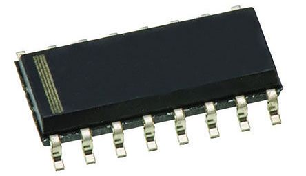
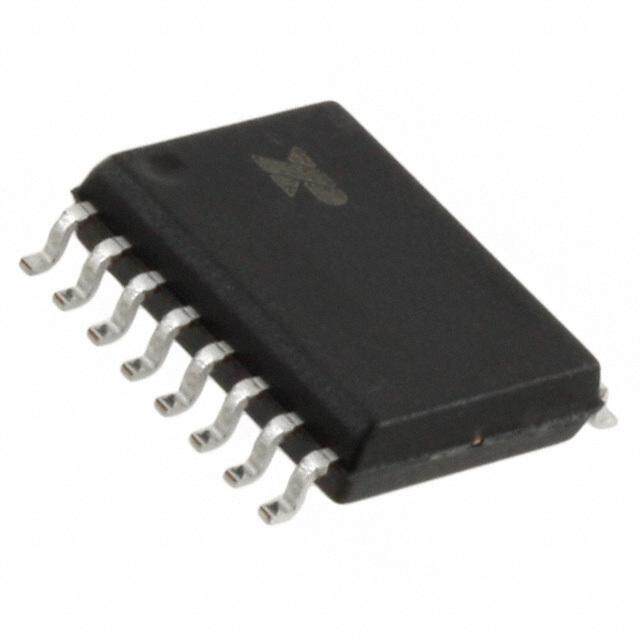
| 产品图片 |
|
| rohs | 符合RoHS无铅 / 符合限制有害物质指令(RoHS)规范要求 |
| 产品系列 | 接口 IC,RS-422接口集成电路,Texas Instruments MC3487D- |
| 数据手册 | |
| 产品型号 | MC3487D |
| 产品目录页面 | |
| 产品种类 | RS-422接口集成电路 |
| 供应商器件封装 | 16-SOIC N |
| 其它名称 | 296-7039-5 |
| 功能 | Transmitter |
| 包装 | 管件 |
| 协议 | RS422 |
| 单位重量 | 141.700 mg |
| 双工 | - |
| 商标 | Texas Instruments |
| 安装类型 | 表面贴装 |
| 安装风格 | SMD/SMT |
| 封装 | Tube |
| 封装/外壳 | 16-SOIC(0.154",3.90mm 宽) |
| 封装/箱体 | SOIC-16 |
| 工作温度 | 0°C ~ 70°C |
| 工作电源电压 | 8 V |
| 工厂包装数量 | 40 |
| 接收器滞后 | - |
| 数据速率 | 10 Mbps |
| 最大工作温度 | + 70 C |
| 最小工作温度 | 0 C |
| 标准包装 | 40 |
| 激励器数量 | 1 |
| 电压-电源 | 4.75 V ~ 5.25 V |
| 电源电流 | 105 mA |
| 类型 | 驱动器 |
| 系列 | MC3487 |
| 驱动器/接收器数 | 4/0 |


- 商务部:美国ITC正式对集成电路等产品启动337调查
- 曝三星4nm工艺存在良率问题 高通将骁龙8 Gen1或转产台积电
- 太阳诱电将投资9.5亿元在常州建新厂生产MLCC 预计2023年完工
- 英特尔发布欧洲新工厂建设计划 深化IDM 2.0 战略
- 台积电先进制程称霸业界 有大客户加持明年业绩稳了
- 达到5530亿美元!SIA预计今年全球半导体销售额将创下新高
- 英特尔拟将自动驾驶子公司Mobileye上市 估值或超500亿美元
- 三星加码芯片和SET,合并消费电子和移动部门,撤换高东真等 CEO
- 三星电子宣布重大人事变动 还合并消费电子和移动部门
- 海关总署:前11个月进口集成电路产品价值2.52万亿元 增长14.8%


PDF Datasheet 数据手册内容提取
(cid:1)(cid:2)(cid:3)(cid:4)(cid:5)(cid:6) (cid:7)(cid:8)(cid:9)(cid:10)(cid:11)(cid:8)(cid:12)(cid:13)(cid:14) (cid:10)(cid:15)(cid:16)(cid:16)(cid:14)(cid:11)(cid:14)(cid:17)(cid:18)(cid:15)(cid:9)(cid:13) (cid:13)(cid:15)(cid:17)(cid:14) (cid:10)(cid:11)(cid:15)(cid:19)(cid:14)(cid:11) SLLS098C − MAY 1980 − REVISED FEBRUARY 2004 (cid:1) Meets or Exceeds Requirements of ANSI D, N, OR NS PACKAGE TIA/EIA-422-B and ITU (TOP VIEW) Recommendation V.11 (cid:1) 1A 1 16 VCC 3-State, TTL-Compatible Outputs 1Y 2 15 4A (cid:1) Fast Transition Times 1Z 3 14 4Y (cid:1) High-Impedance Inputs 1,2EN 4 13 4Z (cid:1) Single 5-V Supply 2Z 5 12 3,4EN (cid:1) 2Y 6 11 3Z Power-Up and Power-Down Protection 2A 7 10 3Y description/ordering information GND 8 9 3A The MC3487 offers four independent differential line drivers designed to meet the specifications of ANSI TIA/EIA-422-B and ITU Recommendation V.11. Each driver has a TTL-compatible input buffered to reduce current and minimize loading. The driver outputs utilize 3-state circuitry to provide high-impedance states at any pair of differential outputs when the appropriate output enable is at a low logic level. Internal circuitry is provided to ensure the high-impedance state at the differential outputs during power-up and power-down transition times, provided the output enable is low. The MC3487 is designed for optimum performance when used with the MC3486 quadruple line receiver. It is supplied in a 16-pin dual-in-line package and operates from a single 5-V supply. ORDERING INFORMATION ORDERABLE TOP-SIDE TA PACKAGE† PART NUMBER MARKING PDIP − N Tube MC3487N MC3487N Tube MC3487D 00°°CC ttoo 7700°°CC SSOOIICC −− DD MMCC33448877 Tape and reel MC3487DR SOP − NS Tape and reel MC3487NSR MC3487 †Package drawings, standard packing quantities, thermal data, symbolization, and PCB design guidelines are available at www.ti.com/sc/package. FUNCTION TABLE (each driver) OOUUTTPPUUTT OUTPUTS IINNPPUUTT ENABLE Y Z H H H L L H L H X L Z Z H = TTL high level, L = TTL low level, X = irrelevant, Z = High impedance Please be aware that an important notice concerning availability, standard warranty, and use in critical applications of TexasInstruments semiconductor products and disclaimers thereto appears at the end of this data sheet. (cid:12)(cid:11)(cid:20)(cid:10)(cid:8)(cid:2)(cid:18)(cid:15)(cid:20)(cid:17) (cid:10)(cid:9)(cid:18)(cid:9) (cid:21)(cid:22)(cid:23)(cid:24)(cid:25)(cid:26)(cid:27)(cid:28)(cid:21)(cid:24)(cid:22) (cid:21)(cid:29) (cid:30)(cid:31)(cid:25)(cid:25)!(cid:22)(cid:28) (cid:27)(cid:29) (cid:24)(cid:23) "(cid:31)#$(cid:21)(cid:30)(cid:27)(cid:28)(cid:21)(cid:24)(cid:22) %(cid:27)(cid:28)!& Copyright 2004, Texas Instruments Incorporated (cid:12)(cid:25)(cid:24)%(cid:31)(cid:30)(cid:28)(cid:29) (cid:30)(cid:24)(cid:22)(cid:23)(cid:24)(cid:25)(cid:26) (cid:28)(cid:24) (cid:29)"!(cid:30)(cid:21)(cid:23)(cid:21)(cid:30)(cid:27)(cid:28)(cid:21)(cid:24)(cid:22)(cid:29) "!(cid:25) (cid:28)’! (cid:28)!(cid:25)(cid:26)(cid:29) (cid:24)(cid:23) (cid:18)!((cid:27)(cid:29) (cid:15)(cid:22)(cid:29)(cid:28)(cid:25)(cid:31)(cid:26)!(cid:22)(cid:28)(cid:29) (cid:29)(cid:28)(cid:27)(cid:22)%(cid:27)(cid:25)% )(cid:27)(cid:25)(cid:25)(cid:27)(cid:22)(cid:28)*& (cid:12)(cid:25)(cid:24)%(cid:31)(cid:30)(cid:28)(cid:21)(cid:24)(cid:22) "(cid:25)(cid:24)(cid:30)!(cid:29)(cid:29)(cid:21)(cid:22)+ %(cid:24)!(cid:29) (cid:22)(cid:24)(cid:28) (cid:22)!(cid:30)!(cid:29)(cid:29)(cid:27)(cid:25)(cid:21)$* (cid:21)(cid:22)(cid:30)$(cid:31)%! (cid:28)!(cid:29)(cid:28)(cid:21)(cid:22)+ (cid:24)(cid:23) (cid:27)$$ "(cid:27)(cid:25)(cid:27)(cid:26)!(cid:28)!(cid:25)(cid:29)& POST OFFICE BOX 655303 • DALLAS, TEXAS 75265 1
(cid:1)(cid:2)(cid:3)(cid:4)(cid:5)(cid:6) (cid:7)(cid:8)(cid:9)(cid:10)(cid:11)(cid:8)(cid:12)(cid:13)(cid:14) (cid:10)(cid:15)(cid:16)(cid:16)(cid:14)(cid:11)(cid:14)(cid:17)(cid:18)(cid:15)(cid:9)(cid:13) (cid:13)(cid:15)(cid:17)(cid:14) (cid:10)(cid:11)(cid:15)(cid:19)(cid:14)(cid:11) SLLS098C − MAY 1980 − REVISED FEBRUARY 2004 logic diagram (positive logic) 4 1,2EN 2 1 1Y 1A 3 1Z 6 7 2Y 2A 5 2Z 12 3,4EN 10 9 3Y 3A 11 3Z 14 15 4Y 4A 13 4Z schematics of inputs and outputs EQUIVALENT OF EACH INPUT TYPICAL OF ALL OUTPUTS VCC VCC Input 9 Ω NOM Output 2 POST OFFICE BOX 655303 • DALLAS, TEXAS 75265
(cid:1)(cid:2)(cid:3)(cid:4)(cid:5)(cid:6) (cid:7)(cid:8)(cid:9)(cid:10)(cid:11)(cid:8)(cid:12)(cid:13)(cid:14) (cid:10)(cid:15)(cid:16)(cid:16)(cid:14)(cid:11)(cid:14)(cid:17)(cid:18)(cid:15)(cid:9)(cid:13) (cid:13)(cid:15)(cid:17)(cid:14) (cid:10)(cid:11)(cid:15)(cid:19)(cid:14)(cid:11) SLLS098C − MAY 1980 − REVISED FEBRUARY 2004 absolute maximum ratings over operating free-air temperature range (unless otherwise noted)† Supply voltage, VCC (see Note 1) . . . . . . . . . . . . . . . . . . . . . . . . . . . . . . . . . . . . . . . . . . . . . . . . . . . . . . . . . . . . . 8 V Input voltage, V . . . . . . . . . . . . . . . . . . . . . . . . . . . . . . . . . . . . . . . . . . . . . . . . . . . . . . . . . . . . . . . . . . . . . . . . . . 5.5 V I Output voltage, V . . . . . . . . . . . . . . . . . . . . . . . . . . . . . . . . . . . . . . . . . . . . . . . . . . . . . . . . . . . . . . . . . . . . . . . . . 7 V O Package thermal impedance, θ (see Notes 2 and 3): D package . . . . . . . . . . . . . . . . . . . . . . . . . . . . 73°C/W JA N package . . . . . . . . . . . . . . . . . . . . . . . . . . . . 67°C/W NS package . . . . . . . . . . . . . . . . . . . . . . . . . . . 64°C/W Operating virtual junction temperature, T . . . . . . . . . . . . . . . . . . . . . . . . . . . . . . . . . . . . . . . . . . . . . . . . . . . 150°C J Storage temperature range, T . . . . . . . . . . . . . . . . . . . . . . . . . . . . . . . . . . . . . . . . . . . . . . . . . . . −65°C to 150°C stg †Stresses beyond those listed under “absolute maximum ratings” may cause permanent damage to the device. These are stress ratings only, and functional operation of the device at these or any other conditions beyond those indicated under “recommended operating conditions” is not implied. Exposure to absolute-maximum-rated conditions for extended periods may affect device reliability. NOTES: 1. All voltage values, except differential output voltage, VOD, are with respect to the network ground terminal. 2. Maximum power dissipation is a function of TJ(max), θJA, and TA. The maximum allowable power dissipation at any allowable ambient temperature is PD = (TJ(max) − TA)/θJA. Operating at the absolute maximum TJ of 150°C can affect reliability. 3. The package thermal impedance is calculated in accordance with JESD 51-7. recommended operating conditions MIN NOM MAX UNIT VCC Supply voltage 4.75 5 5.25 V VIH High-level input voltage 2 V VIL Low-level input voltage 0.8 V TA Operating free-air temperature 0 70 °C POST OFFICE BOX 655303 • DALLAS, TEXAS 75265 3
(cid:1)(cid:2)(cid:3)(cid:4)(cid:5)(cid:6) (cid:7)(cid:8)(cid:9)(cid:10)(cid:11)(cid:8)(cid:12)(cid:13)(cid:14) (cid:10)(cid:15)(cid:16)(cid:16)(cid:14)(cid:11)(cid:14)(cid:17)(cid:18)(cid:15)(cid:9)(cid:13) (cid:13)(cid:15)(cid:17)(cid:14) (cid:10)(cid:11)(cid:15)(cid:19)(cid:14)(cid:11) SLLS098C − MAY 1980 − REVISED FEBRUARY 2004 electrical characteristics over recommended ranges of supply voltage and operating free-air temperature (unless otherwise noted) PARAMETER TEST CONDITIONS MIN MAX UNIT VIK Input clamp voltage II = −18 mA −1.5 V VOH High-level output voltage VIL = 0.8 V, VIH = 2 V, IOH = −20 mA 2.5 V VOL Low-level output voltage VIL = 0.8 V, VIH = 2 V, IOL = 48 mA 0.5 V |VOD| Differential output voltage RL = 100 Ω, See Figure 1 2 CChhaannggee iinn mmaaggnniittuuddee ooff ∆∆||VVOODD|| differential output voltage†† RRLL == 110000 ΩΩ,, SSeeee FFiigguurree 11 ±±00..44 VV VOC Common-mode output voltage‡ RL = 100 Ω, See Figure 1 3 V CChhaannggee iinn mmaaggnniittuuddee ooff ∆∆||VVOOCC|| common-mode output voltage†† RRLL == 110000 ΩΩ,, SSeeee FFiigguurree 11 ±±00..44 VV VO = 6 V 100 IIOO OOuuttppuutt ccuurrrreenntt wwiitthh ppoowweerr ooffff VVCCCC == 00 µAA VO = −0.25 V −100 VO = 2.7 V 100 IIOOZZ HHiigghh--iimmppeeddaannccee--ssttaattee oouuttppuutt ccuurrrreenntt OOuuttppuutt eennaabblleess aatt 00..88 VV µAA VO = 0.5 V −100 Input current at maximum input II voltage VI = 5.5 V 100 µA IIH High-level input current VI = 2.7 V 50 µA IIL Low-level input current VI = 0.5 V −400 µA IOS Short-circuit output current§ VI = 2 V −40 −140 mA Outputs disabled 105 IICCCC SSuuppppllyy ccuurrrreenntt ((aallll ddrriivveerrss)) mmAA Outputs enabled, No load 85 †∆|VOD| and ∆|VOC| are the changes in magnitude of VOD and VOC, respectively, that occur when the input is changed from a high level to a low level. ‡In ANSI Standard TIA/EIA-422-B, VOC, which is the average of the two output voltages with respect to ground, is called output offset voltage, VOS. §Only one output at a time should be shorted, and duration of the short circuit should not exceed one second. switching characteristics over recommended operating free-air temperature range, V = 5 V CC PARAMETER TEST CONDITIONS MIN MAX UNIT tPLH Propagation delay time, low- to high-level output 20 CCLL == 1155 ppFF,, SSeeee FFiigguurree 22 nnss tPHL Propagation delay time, high- to low-level output 20 tsk Skew time CL = 15 pF, See Figure 2 6 ns tt(OD) Differential-output transition time CL = 15 pF, See Figure 3 20 ns tPZH Output enable time to high level 30 CCLL == 5500 ppFF,, SSeeee FFiigguurree 44 nnss tPZL Output enable time to low level 30 tPHZ Output disable time from high level 25 CCLL == 5500 ppFF,, SSeeee FFiigguurree 44 nnss tPLZ Output disable time from low level 30 4 POST OFFICE BOX 655303 • DALLAS, TEXAS 75265
(cid:1)(cid:2)(cid:3)(cid:4)(cid:5)(cid:6) (cid:7)(cid:8)(cid:9)(cid:10)(cid:11)(cid:8)(cid:12)(cid:13)(cid:14) (cid:10)(cid:15)(cid:16)(cid:16)(cid:14)(cid:11)(cid:14)(cid:17)(cid:18)(cid:15)(cid:9)(cid:13) (cid:13)(cid:15)(cid:17)(cid:14) (cid:10)(cid:11)(cid:15)(cid:19)(cid:14)(cid:11) SLLS098C − MAY 1980 − REVISED FEBRUARY 2004 PARAMETER MEASUREMENT INFORMATION 50 Ω VOD 50 Ω VOC Figure 1. Differential and Common-Mode Output Voltages 3 V Input 1.5 V 1.5 V 0 V tPLH tPHL 5 V VOH Y Output 1.5 V 1.5 V 200 Ω SW1 VOL Generator 50 Ω Skew Skew (see Note A) ÏÏÏ CL = 15 pF tPHL tPLH (see Note B) ÏÏÏ VOH 3 V Z Output 1.5 V 1.5 V See Note C VOL TEST CIRCUIT VOLTAGE WAVEFORMS NOTES: A. The input pulse is supplied by a generator having the following characteristics: tr ≤ 5 ns, tf ≤ 5 ns, PRR ≤ 1 MHz, duty cycle = 50%, ZO = 50 Ω. B. CL includes probe and stray capacitance. C. All diodes are 1N916 or 1N3064. Figure 2. Test Circuit and Voltage Waveforms 3 V CL RL = 100 Ω Input Generator Output 0 V (see Note A) 50 Ω tt(OD) tt(OD) 3 V CL = 15 pF Output 90% (see Note B) 10% TEST CIRCUIT VOLTAGE WAVEFORMS NOTES: A. The input pulse is supplied by a generator having the following characteristics: tr ≤ 5 ns, tf ≤ 5 ns, PRR ≤ 1 MHz, duty cycle = 50%, ZO = 50 Ω. B. CL includes probe and stray capacitance. Figure 3. Test Circuit and Voltage Waveforms POST OFFICE BOX 655303 • DALLAS, TEXAS 75265 5
(cid:1)(cid:2)(cid:3)(cid:4)(cid:5)(cid:6) (cid:7)(cid:8)(cid:9)(cid:10)(cid:11)(cid:8)(cid:12)(cid:13)(cid:14) (cid:10)(cid:15)(cid:16)(cid:16)(cid:14)(cid:11)(cid:14)(cid:17)(cid:18)(cid:15)(cid:9)(cid:13) (cid:13)(cid:15)(cid:17)(cid:14) (cid:10)(cid:11)(cid:15)(cid:19)(cid:14)(cid:11) SLLS098C − MAY 1980 − REVISED FEBRUARY 2004 PARAMETER MEASUREMENT INFORMATION 5 V Output 200 Ω SW3 SW1 0 V or 3 V CL = 15 pF 1 kΩ See Note C Generator (see Note B) (see Note A) 50 Ω SW2 TEST CIRCUIT Output 3 V Output 3 V Enable Input 1.5 V Enable Input 1.5 V 0 V 0 V tPHZ tPZL SW1 Closed VOH 0.5 V SW1 Closed SW2 Open 1.5 V Output SW2 Closed Output ≈1.5 V VOL tPLZ ≈1.5 V tPZH VOH Output 0.5 V SSWW21 CClloosseedd Output 1.5 V SW1 Open VOL SW2 Closed VOLTAGE WAVEFORMS NOTES: A. The input pulse is supplied by a generator having the following characteristics: tr ≤ 5 ns, tf ≤ 5 ns, PRR ≤ 1 MHz, duty cycle = 50%, ZO = 50 Ω. B. CL includes probe and stray capacitance. C. All diodes are 1N916 or 1N3064. Figure 4. Driver Test Circuit and Voltage Waveforms 6 POST OFFICE BOX 655303 • DALLAS, TEXAS 75265
PACKAGE OPTION ADDENDUM www.ti.com 6-Feb-2020 PACKAGING INFORMATION Orderable Device Status Package Type Package Pins Package Eco Plan Lead/Ball Finish MSL Peak Temp Op Temp (°C) Device Marking Samples (1) Drawing Qty (2) (6) (3) (4/5) MC3487D ACTIVE SOIC D 16 40 Green (RoHS NIPDAU Level-1-260C-UNLIM 0 to 70 MC3487 & no Sb/Br) MC3487DE4 ACTIVE SOIC D 16 40 Green (RoHS NIPDAU Level-1-260C-UNLIM 0 to 70 MC3487 & no Sb/Br) MC3487DR ACTIVE SOIC D 16 2500 Green (RoHS NIPDAU Level-1-260C-UNLIM 0 to 70 MC3487 & no Sb/Br) MC3487DRE4 ACTIVE SOIC D 16 2500 Green (RoHS NIPDAU Level-1-260C-UNLIM 0 to 70 MC3487 & no Sb/Br) MC3487N ACTIVE PDIP N 16 25 Green (RoHS NIPDAU N / A for Pkg Type 0 to 70 MC3487N & no Sb/Br) MC3487NE4 ACTIVE PDIP N 16 25 Green (RoHS NIPDAU N / A for Pkg Type 0 to 70 MC3487N & no Sb/Br) MC3487NSR ACTIVE SO NS 16 2000 Green (RoHS NIPDAU Level-1-260C-UNLIM 0 to 70 MC3487 & no Sb/Br) (1) The marketing status values are defined as follows: ACTIVE: Product device recommended for new designs. LIFEBUY: TI has announced that the device will be discontinued, and a lifetime-buy period is in effect. NRND: Not recommended for new designs. Device is in production to support existing customers, but TI does not recommend using this part in a new design. PREVIEW: Device has been announced but is not in production. Samples may or may not be available. OBSOLETE: TI has discontinued the production of the device. (2) RoHS: TI defines "RoHS" to mean semiconductor products that are compliant with the current EU RoHS requirements for all 10 RoHS substances, including the requirement that RoHS substance do not exceed 0.1% by weight in homogeneous materials. Where designed to be soldered at high temperatures, "RoHS" products are suitable for use in specified lead-free processes. TI may reference these types of products as "Pb-Free". RoHS Exempt: TI defines "RoHS Exempt" to mean products that contain lead but are compliant with EU RoHS pursuant to a specific EU RoHS exemption. Green: TI defines "Green" to mean the content of Chlorine (Cl) and Bromine (Br) based flame retardants meet JS709B low halogen requirements of <=1000ppm threshold. Antimony trioxide based flame retardants must also meet the <=1000ppm threshold requirement. (3) MSL, Peak Temp. - The Moisture Sensitivity Level rating according to the JEDEC industry standard classifications, and peak solder temperature. (4) There may be additional marking, which relates to the logo, the lot trace code information, or the environmental category on the device. (5) Multiple Device Markings will be inside parentheses. Only one Device Marking contained in parentheses and separated by a "~" will appear on a device. If a line is indented then it is a continuation of the previous line and the two combined represent the entire Device Marking for that device. Addendum-Page 1
PACKAGE OPTION ADDENDUM www.ti.com 6-Feb-2020 (6) Lead/Ball Finish - Orderable Devices may have multiple material finish options. Finish options are separated by a vertical ruled line. Lead/Ball Finish values may wrap to two lines if the finish value exceeds the maximum column width. Important Information and Disclaimer:The information provided on this page represents TI's knowledge and belief as of the date that it is provided. TI bases its knowledge and belief on information provided by third parties, and makes no representation or warranty as to the accuracy of such information. Efforts are underway to better integrate information from third parties. TI has taken and continues to take reasonable steps to provide representative and accurate information but may not have conducted destructive testing or chemical analysis on incoming materials and chemicals. TI and TI suppliers consider certain information to be proprietary, and thus CAS numbers and other limited information may not be available for release. In no event shall TI's liability arising out of such information exceed the total purchase price of the TI part(s) at issue in this document sold by TI to Customer on an annual basis. Addendum-Page 2
PACKAGE MATERIALS INFORMATION www.ti.com 6-Dec-2019 TAPE AND REEL INFORMATION *Alldimensionsarenominal Device Package Package Pins SPQ Reel Reel A0 B0 K0 P1 W Pin1 Type Drawing Diameter Width (mm) (mm) (mm) (mm) (mm) Quadrant (mm) W1(mm) MC3487DR SOIC D 16 2500 330.0 16.4 6.5 10.3 2.1 8.0 16.0 Q1 MC3487DR SOIC D 16 2500 330.0 16.4 6.5 10.3 2.1 8.0 16.0 Q1 MC3487NSR SO NS 16 2000 330.0 16.4 8.2 10.5 2.5 12.0 16.0 Q1 PackMaterials-Page1
PACKAGE MATERIALS INFORMATION www.ti.com 6-Dec-2019 *Alldimensionsarenominal Device PackageType PackageDrawing Pins SPQ Length(mm) Width(mm) Height(mm) MC3487DR SOIC D 16 2500 333.2 345.9 28.6 MC3487DR SOIC D 16 2500 367.0 367.0 38.0 MC3487NSR SO NS 16 2000 367.0 367.0 38.0 PackMaterials-Page2
None
None
None
None
IMPORTANTNOTICEANDDISCLAIMER TI PROVIDES TECHNICAL AND RELIABILITY DATA (INCLUDING DATASHEETS), DESIGN RESOURCES (INCLUDING REFERENCE DESIGNS), APPLICATION OR OTHER DESIGN ADVICE, WEB TOOLS, SAFETY INFORMATION, AND OTHER RESOURCES “AS IS” AND WITH ALL FAULTS, AND DISCLAIMS ALL WARRANTIES, EXPRESS AND IMPLIED, INCLUDING WITHOUT LIMITATION ANY IMPLIED WARRANTIES OF MERCHANTABILITY, FITNESS FOR A PARTICULAR PURPOSE OR NON-INFRINGEMENT OF THIRD PARTY INTELLECTUAL PROPERTY RIGHTS. These resources are intended for skilled developers designing with TI products. You are solely responsible for (1) selecting the appropriate TI products for your application, (2) designing, validating and testing your application, and (3) ensuring your application meets applicable standards, and any other safety, security, or other requirements. These resources are subject to change without notice. TI grants you permission to use these resources only for development of an application that uses the TI products described in the resource. Other reproduction and display of these resources is prohibited. No license is granted to any other TI intellectual property right or to any third party intellectual property right. TI disclaims responsibility for, and you will fully indemnify TI and its representatives against, any claims, damages, costs, losses, and liabilities arising out of your use of these resources. TI’s products are provided subject to TI’s Terms of Sale (www.ti.com/legal/termsofsale.html) or other applicable terms available either on ti.com or provided in conjunction with such TI products. TI’s provision of these resources does not expand or otherwise alter TI’s applicable warranties or warranty disclaimers for TI products. Mailing Address: Texas Instruments, Post Office Box 655303, Dallas, Texas 75265 Copyright © 2020, Texas Instruments Incorporated