ICGOO在线商城 > 集成电路(IC) > PMIC - 稳压器 - 线性 > MC33269DT-5.0G
 Datasheet下载
- 型号: MC33269DT-5.0G
- 制造商: ON Semiconductor
- 库位|库存: xxxx|xxxx
- 要求:
| 数量阶梯 | 香港交货 | 国内含税 |
| +xxxx | $xxxx | ¥xxxx |
查看当月历史价格
查看今年历史价格
MC33269DT-5.0G产品简介:
ICGOO电子元器件商城为您提供MC33269DT-5.0G由ON Semiconductor设计生产,在icgoo商城现货销售,并且可以通过原厂、代理商等渠道进行代购。 MC33269DT-5.0G价格参考¥0.16-¥0.16。ON SemiconductorMC33269DT-5.0G封装/规格:PMIC - 稳压器 - 线性, Linear Voltage Regulator IC Positive Fixed 1 Output 5V 800mA DPAK。您可以下载MC33269DT-5.0G参考资料、Datasheet数据手册功能说明书,资料中有MC33269DT-5.0G 详细功能的应用电路图电压和使用方法及教程。
MC33269DT-5.0G 是一款由 ON Semiconductor(安森美半导体)生产的线性稳压器,属于 PMIC(电源管理集成电路)类别。它是一种低压差线性稳压器(LDO),能够提供稳定的 5.0V 输出电压,适用于多种电子设备和应用场景。

 应用场景:

1. 消费类电子产品
   - 手持设备:如便携式媒体播放器、电子书阅读器等,需要稳定电源的设备。
   - 遥控器:为红外遥控器或其他无线遥控设备提供稳定的供电。
   - 数码相机:为相机内部的传感器和其他低功耗组件供电。

2. 工业应用
   - 数据采集系统:为传感器模块或信号调理电路提供精确的电源。
   - 嵌入式控制器:在工业自动化设备中,为微控制器单元(MCU)或其他低功耗芯片供电。
   - 测量仪器:如数字万用表、示波器等需要高精度电源的应用。

3. 通信设备
   - 有线/无线通信模块:为蓝牙、Wi-Fi 或 Zigbee 模块提供稳定的电源。
   - 路由器与调制解调器:为低功耗子系统供电,确保信号传输的稳定性。

4. 汽车电子
   - 车载信息娱乐系统:为导航、音频系统中的低功耗部分供电。
   - 传感器模块:为温度、压力等车载传感器提供稳定的电源支持。

5. 医疗设备
   - 可穿戴健康设备:如智能手环、心率监测仪等需要低功耗电源的设备。
   - 便携式医疗仪器:如血糖仪、血氧仪等,对电源稳定性和效率要求较高的场合。

6. 物联网(IoT)设备
   - 智能家居设备:如智能灯泡、温控器等需要长时间稳定运行的小型设备。
   - 环境监测节点:为气象站或环境传感器提供可靠的电源支持。

 特点:
- 输出电压固定为 5.0V,适合为 USB 接口或其他 5V 供电的设备供电。
- 具有较低的压差特性,可提高整体系统的能效。
- 内置过流保护和热关断功能,确保在异常情况下不会损坏设备。

综上所述,MC33269DT-5.0G 广泛应用于需要稳定 5V 电源的各种场景,尤其适合对成本敏感且对性能有一定要求的低功耗产品设计。
| 参数 | 数值 |
| 产品目录 | 集成电路 (IC)半导体 |
| 描述 | IC REG LDO 5V 0.8A DPAK低压差稳压器 5.0V ADJ 800mA |
| 产品分类 | |
| 品牌 | ON Semiconductor |
| 产品手册 | |
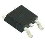
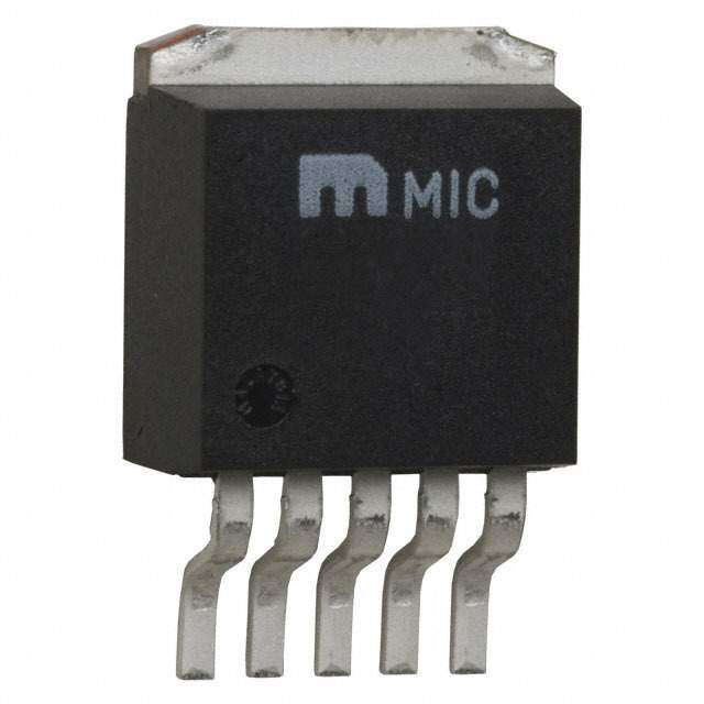
| 产品图片 |
|
| rohs | 符合RoHS无铅 / 符合限制有害物质指令(RoHS)规范要求 |
| 产品系列 | 电源管理 IC,低压差稳压器,ON Semiconductor MC33269DT-5.0G- |
| 数据手册 | |
| 产品型号 | MC33269DT-5.0G |
| 产品目录页面 | |
| 产品种类 | 低压差稳压器 |
| 供应商器件封装 | DPAK-3 |
| 其它名称 | MC33269DT-5.0G-ND |
| 包装 | 管件 |
| 商标 | ON Semiconductor |
| 回动电压—最大值 | 1.25 V at 500 mA |
| 安装类型 | 表面贴装 |
| 安装风格 | SMD/SMT |
| 封装 | Tube |
| 封装/外壳 | TO-252-3,DPak(2 引线+接片),SC-63 |
| 封装/箱体 | TO-252-3 (DPAK) |
| 工作温度 | -40°C ~ 125°C |
| 工厂包装数量 | 75 |
| 最大工作温度 | + 125 C |
| 最大输入电压 | 20 V |
| 最小工作温度 | - 40 C |
| 标准包装 | 75 |
| 电压-跌落(典型值) | 1.1V @ 800mA |
| 电压-输入 | 最高 20V |
| 电压-输出 | 5V |
| 电压调节准确度 | 1 % |
| 电流-输出 | 800mA |
| 电流-限制(最小值) | 800mA |
| 稳压器拓扑 | 正,固定式 |
| 稳压器数 | 1 |
| 系列 | MC33269 |
| 线路调整率 | 0.3 % |
| 负载调节 | 0.5 % |
| 输出电压 | 5 V |
| 输出电流 | 800 mA |
| 输出端数量 | 1 Output |
| 输出类型 | Fixed |


- 商务部:美国ITC正式对集成电路等产品启动337调查
- 曝三星4nm工艺存在良率问题 高通将骁龙8 Gen1或转产台积电
- 太阳诱电将投资9.5亿元在常州建新厂生产MLCC 预计2023年完工
- 英特尔发布欧洲新工厂建设计划 深化IDM 2.0 战略
- 台积电先进制程称霸业界 有大客户加持明年业绩稳了
- 达到5530亿美元!SIA预计今年全球半导体销售额将创下新高
- 英特尔拟将自动驾驶子公司Mobileye上市 估值或超500亿美元
- 三星加码芯片和SET,合并消费电子和移动部门,撤换高东真等 CEO
- 三星电子宣布重大人事变动 还合并消费电子和移动部门
- 海关总署:前11个月进口集成电路产品价值2.52万亿元 增长14.8%


PDF Datasheet 数据手册内容提取
MC33269, NCV33269 800 mA, Adjustable Output, Low Dropout Voltage Regulator The MC33269/NCV33269 series are low dropout, medium current, fixed and adjustable, positive voltage regulators specifically designed http://onsemi.com for use in low input voltage applications. These devices offer the circuit designer an economical solution for precision voltage SO−8 regulation, while keeping power losses to a minimum. 8 D SUFFIX The regulator consists of a 1.0 V dropout composite PNP−NPN pass 1 CASE 751 transistor, current limiting, and thermal shutdown. GND/Adj 1 8 NC Features • 2 7 3.3 V, 3.5 V, 5.0 V, 12 V and Adjustable Versions Vout Vout 2.85 V version available as MC34268 3 6 • Space Saving DPAK, SO−8 and SOT−223 Power Packages Vin 4 5 NC • 1.0 V Dropout (Top View) • Output Current in Excess of 800 mA • Thermal Protection DPAK • DT SUFFIX Short Circuit Protection CASE 369C • Output Trimmed to 1.0% Tolerance 1 1 2 3 • 3 NCV Prefix for Automotive and Other Applications Requiring 1. GND/Adj Unique Site and Control Change Requirements; AEC−Q100 2. Vout (Top View) 3. Vin Qualified and PPAP Capable • These are Pb−Free Devices SOT−223 1 ST SUFFIX 1 2 3 3 CASE 318E (Top View) DEVICE TYPE/NOMINAL OUTPUT VOLTAGE Heatsink surface (shown as terminal 4 in case outline drawing) is connected to Pin 2. MC33269D Adj MC33269T−3.5 3.5 V NCV33269D* Adj MC33269D−5.0 5.0 V MC33269DT Adj MC33269DT−5.0 5.0 V NCV33269DTRK* Adj NCV33269DT−5.0* 5.0 V TO−220AB MC33269T Adj NCV33269DTRK−5.0* 5.0 V T SUFFIX MC33269D−3.3 3.3 V MC33269T−5.0 5.0 V CASE 221AB MC33269DT−3.3 3.3 V MC33269D−012 12 V 1. GND/Adj NCV33269DTRK−3.3* 3.3 V MC33269DT−012 12 V 2. Vout MC33269T−3.3 3.3 V NCV33269DTRK−012* 12 V 12 3. Vin 123 MC33269ST−3.3 3.3 V MC33269T−012 12 V 3 (Top View) *NCV Prefix for Automotive and Other Applications Requiring Unique Site and Heatsink surface (shown as terminal 4 in Control Change Requirements; AEC−Q100 Qualified and PPAP Capable. case outline drawing) is connected to Pin 2. ORDERING INFORMATION See detailed ordering and shipping information in the package dimensions section on page 7 of this data sheet. DEVICE MARKING INFORMATION See general marking information in the device marking section on page 8 of this data sheet. © Semiconductor Components Industries, LLC, 2014 1 Publication Order Number: August, 2014 − Rev. 28 MC33269/D
MC33269, NCV33269 MAXIMUM RATINGS Rating Symbol Value Unit Power Supply Input Voltage Vin 20 V Power Dissipation Case 369C (DPAK) TA = 25°C PD Internally Limited W Thermal Resistance, Junction−to−Ambient (cid:2) 92 °C/W JA Thermal Resistance, Junction−to−Case (cid:2) 6.0 °C/W JC Case 751 (SO−8) TA = 25°C PD Internally Limited W Thermal Resistance, Junction−to−Ambient (cid:2) 160 °C/W JA Thermal Resistance, Junction−to−Case (cid:2) 25 °C/W JC Case 221A (TO−220) TA = 25°C PD Internally Limited W Thermal Resistance, Junction−to−Ambient (cid:2) 65 °C/W JA Thermal Resistance, Junction−to−Case (cid:2) 5.0 °C/W JC Case 318E (SOT−223) TA = 25°C PD Internally Limited W Thermal Resistance, Junction−to−Ambient (cid:2) 156 °C/W JA Thermal Resistance, Junction−to−Case (cid:2) 15 °C/W JC Operating Die Junction Temperature Range TJ −40 to +150 °C Operating Ambient Temperature Range MC33269 TA −40 to +125 °C NCV33269 −40 to +125 Storage Temperature Tstg −55 to +150 °C Electrostatic Discharge Sensitivity (ESD) Human Body Model (HBM) ESD 4000 V Machine Model (MM) 400 Stresses exceeding Maximum Ratings may damage the device. Maximum Ratings are stress ratings only. Functional operation above the Recommended Operating Conditions is not implied. Extended exposure to stresses above the Recommended Operating Conditions may affect device reliability. ELECTRICAL CHARACTERISTICS (CO = 10 (cid:3)F, TA = 25°C, for min/max values TA = −40°C to +125°C, unless otherwise noted.) Characteristic Symbol Min Typ Max Unit Output Voltage (Iout = 10 mA, TA = 25°C) VO V 3.3 Suffix (VCC = 5.3 V) 3.27 3.3 3.33 3.5 Suffix (VCC = 5.5 V) 3.465 3.5 3.535 5.0 Suffix (VCC = 7.0 V) 4.95 5.0 5.05 12 Suffix (VCC = 14 V) 11.88 12 12.12 Output Voltage (Line, Load and Temperature) (Note 1) VO V (1.25 V ≤ Vin − Vout ≤ 15 V, Iout = 500 mA) (1.35 V ≤ Vin − Vout ≤ 10 V, Iout = 800 mA) 3.3 Suffix 3.23 3.3 3.37 3.5 Suffix 3.43 3.5 3.57 5.0 Suffix 4.90 5.0 5.10 12 Suffix 11.76 12 12.24 Reference Voltage for Adjustable Voltage Vref 1.235 1.25 1.265 V (Iout = 10 mA, Vin − Vout = 2.0 V, TA = 25°C) Reference Voltage (Line, Load and Temperature) (Note 1) for Adjustable Voltage Vref 1.225 1.25 1.275 V (1.25 V ≤ Vin − Vout ≤ 15 V, Iout = 500 mA) (1.35 V ≤ Vin − Vout ≤ 10 V, Iout = 800 mA) Line Regulation (Iout = 10 mA, Vin = [Vout + 1.5 V] to Vin = 20 V, TA = 25°C) Regline − − 0.3 % Load Regulation (Vin = Vout + 3.0 V, Iout = 10 mA to 800 mA, TA = 25°C) Regload − − 0.5 % Dropout Voltage (Iout = 500 mA) Vin−Vout − 1.0 1.25 V (Iout = 800 mA) − 1.1 1.35 Ripple Rejection (10 Vpp, 120 Hz Sinewave; Iout = 500 mA) RR 55 − − dB Current Limit (Vin − Vout = 10 V) ILimit 800 − − mA Quiescent Current (Fixed Output) (1.5 V ≤ Vout ≤ 3.5 V) IQ − 5.5 8.0 mA (5 V ≤ Vout ≤ 12 V) − − 20 Minimum Required Load Current Fixed Output Voltage ILoad − − 0 mA Adjustable Voltage 8.0 − − Adjustment Pin Current IAdj − − 120 (cid:3)A 1. The MC33269−12, Vin − Vout is limited to 8.0 V maximum, because of the 20 V maximum rating applied to Vin. http://onsemi.com 2
MC33269, NCV33269 Vin Vout Trim Links VAdj Gnd This device contains 38 active transistors. Figure 1. Internal Schematic http://onsemi.com 3
MC33269, NCV33269 1.5 N V) O POUT VOLTAGE ( 11..31 TA = 25°C TA = -40°C ΔV, OUTPUTOOLTAGE DEVIATI Cin = 10 (cid:3)F 1m0V0/Div RO 0.9 TA = 125°C V CO = 10 (cid:3)F Tantalum , Dut UTT VPirne l=o aVdO =+ 0 3.1.0 A V V-Vino 0.7 , OUTPOCURREN 0.5 A 0.5 I 0 A 0 200 400 600 800 1000 20 ms/DIV IO, OUTPUT LOAD CURRENT (mA) Figure 2. Dropout Voltage versus Figure 3. Transient Load Regulation Output Load Current V )FB % 1100 1.6 D ( OL IO = 800 mA 1.4 RESH1060 T (A) 1.2 H N UT T1020 RRE 1.0 TA = 25°C P U MC33269D-XX N C 0.8 OLTAGE I 980 OUTPUT 0.6 L = 25 mm Copper V 0.4 R 940 E OV 0.2 , V) O 900 0 B( -55 -25 0 25 50 75 100 125 0 2.0 4.0 6.0 8.0 10 12 14 16 F V TA, AMBIENT TEMPERATURE (°C) INPUT-OUTPUT VOLTAGE DIFFERENTIAL (V) Figure 4. Dropout Voltage Figure 5. MC33269−XX Output DC Current versus versus Temperature Input−Output Differential Voltage 70 70 B) VO = 3.3 V or 5.0 V B) d d O ( 60 O ( 60 ATI VO = 12 V ATI R R N N O 50 O 50 CTI CTI Vin = 8.0 V JE JE Vout = 5.0 V RE 40 Vin = VO + 3.0 V RE 40 IL = 800 mA PPLE TILA = = 8 2050° mCA PPLE CTAA d=j =2 52°2C (cid:3)F RI 30 RI 30 R, R, R R 20 20 0.1 1.0 10 100 0.1 1.0 10 100 f, FREQUENCY (kHz) f, FREQUENCY (kHz) Figure 6. MC33269 Ripple Rejection Figure 7. MC33269−ADJ Ripple Rejection versus Frequency versus Frequency http://onsemi.com 4
MC33269, NCV33269 170 3.2 NCE, W) 150 PD(max) for TA = 50°C 2.8 SISTA°R ( C/ 130 2.4 RE -AI 110 Graph represents symmetrical layout 2.0 L O ÏÏÏ ÏÏÏ A T HERM TION- 90 ÏL CÏ2.o0p opzeÏÏ.r ÏÏÏÏÏ 1.6 , TθJAJUNC 70 ÏÏLÏ ÏÏ3.0Ï mm 1.2 R 50 0.8 R(cid:2)JA 30 0.4 0 10 20 30 40 50 L, LENGTH OF COPPER (mm) Figure 8. SOP−8 Thermal Resistance and Maximum Power Dissipation versus P.C.B. Copper Length 100 2.4 Free Air PD(max) for TA = 50°C E, 90 Mounted 2.0 NC W) Vertically SISTA °R ( C/ 80 Ï2.0 ozÏ. CLopÏper 1.6 RE AI Minimum ÏÏÏ MAL -TO- 70 Size Pad LÏÏÏ 1.2 R N E O , THANCTI 60 ÏÏÏ 0.8 JU Rθ J 50 0.4 R(cid:2)JA 40 0 0 5.0 10 15 20 25 30 L, LENGTH OF COPPER (mm) Figure 9. DPAK Thermal Resistance and Maximum Power Dissipation versus P.C.B. Copper Length 280 Free Air PD(max) for TA = 50°C 2.50 N (W) ESISTANCE°R ( C/W) 220400 VMeoruticnatelldy Ï2.0 oÏz. CLoÏpperÏ01..8235 DISSIPATIO , THERMAL RJAUNCTION‐TO‐AI 112600 MSiizneim Puamd ÏÏL ÏÏÏÏÏÏ00..5603 XIMUM POWER θ J A R 80 0.42 M R(cid:2)JA P, D 40 0.35 0 5.0 10 15 20 25 30 L, LENGTH OF COPPER (mm) Figure 10. SOT−223 Thermal Resistance and Maximum Power Dissipation versus P.C.B. Copper Length http://onsemi.com 5
MC33269, NCV33269 APPLICATIONS INFORMATION Figures 11 through 15 are typical application circuits. The supply input filter with long wire lengths. This will reduce output current capability of the regulator is in excess of the circuit’s sensitivity to the input line impedance at high 800 mA, with a typical dropout voltage of less than 1.0 V. frequencies. A 0.33 (cid:3)F or larger tantalum, mylar, ceramic, Internal protective features include current and thermal or other capacitor having low internal impedance at high limiting. frequencies should be chosen. The bypass capacitor should * The MC33269 requires an external output capacitor for be mounted with shortest possible lead or track length stability. The capacitor should be at least 10 (cid:3)F with an directly across the regulator’s input terminals. Applications equivalent series resistance (ESR) of less than 10 (cid:4) but should be tested over all operating conditions to insure greater than 0.2 (cid:4) over the anticipated operating stability. temperature range. With economical electrolytic capacitors, Internal thermal limiting circuitry is provided to protect cold temperature operation can pose a problem. As the integrated circuit in the event that the maximum junction temperature decreases, the capacitance also decreases and temperature is exceeded. When activated, typically at the ESR increases, which could cause the circuit to oscillate. 170°C, the output is disabled. There is no hysteresis built Also capacitance and ESR of a solid tantalum capacitor is into the thermal limiting circuit. As a result, if the device is more stable over temperature. The use of a low ESR ceramic overheating, the output will appear to be oscillating. This capacitor placed within close proximity to the output of the feature is provided to prevent catastrophic failures from device could cause instability. accidental device overheating. It is not intended to be used ** An input bypass capacitor is recommended to improve as a substitute for proper heat−sinking. transient response or if the regulator is connected to the Vin Vout Vin Vout MC33269-XX MC33269 **Cin C10o *(cid:3)F **Cin Adj R1 Co* GND 10 (cid:3)F R2 An input capacitor is not necessary for stability, however CAdj*** it will improve the overall performance. Figure 11. Typical Fixed Output Application (cid:3) (cid:5) V (cid:3)(cid:2)(cid:3)1.25(cid:3)(cid:3) 1(cid:4)R2 (cid:3)(cid:4)(cid:3)I R2 out R1 Adj(cid:3) ***CAdj is optional, however it will improve the ripple rejection. Vin RS Iout The MC34269 develops a 1.25 V reference voltage between the MC33269 output and the adjust terminal. Resistor R1, operates with **Cin C10o *(cid:3)F constant current to flow through it and resistor R2. This current Adj should be set such that the Adjust Pin current causes negligible drop across resistor R2. The total current with minimum load I (cid:3)(cid:2)(cid:3)1.25 should be greater than 8.0 mA. out R S Figure 13. Current Regulator Figure 12. Typical Adjustable Output Application Vin Vout MC33269-XX **Cin Vin Vout MC33269 GND **Cin R1 Adj Co* 10 (cid:3)F R2 MC33269-XX **Cin C10o *(cid:3)F GND The Schottky diode in series with the ground leg of the upper regulator shifts its output voltage higher by the forward voltage drop of the diode. This will cause the lower device R2 sets the maximum output voltage. Each transistor to remain off until the input voltage is removed. reduces the output voltage when turned on. Figure 14. Battery Backed−Up Power Supply Figure 15. Digitally Controlled Voltage Regulator http://onsemi.com 6
MC33269, NCV33269 ORDERING INFORMATION Device Package Shipping Information† MC33269DG SO−8 98 Units / Rail (Pb−Free) MC33269DR2G SO−8 2500 Units / Tape & Reel (Pb−Free) MC33269DTG DPAK 75 Units / Rail (Pb−Free) MC33269DTRKG DPAK 2500 Units / Tape & Reel (Pb−Free) MC33269TG TO−220 50 Units / Rail (Pb−Free) MC33269D−3.3G SO−8 98 Units / Rail (Pb−Free) MC33269DR2−3.3G SO−8 2500 Units / Tape & Reel (Pb−Free) MC33269DT−3.3G DPAK 75 Units / Rail (Pb−Free) MC33269DTRK−3.3G DPAK 2500 Units / Tape & Reel (Pb−Free) MC33269ST−3.3T3G SOT−223 4000 Units / Tape & Reel (Pb−Free) MC33269T−3.3G TO−220 50 Units / Rail (Pb−Free) MC33269T−3.5G TO−220 50 Units / Rail (Pb−Free) MC33269D−5.0G SO−8 98 Units / Rail (Pb−Free) MC33269DR2−5.0G SO−8 2500 Units / Tape & Reel (Pb−Free) MC33269DT−5.0G DPAK 75 Units / Rail (Pb−Free) NCV33269DT−5.0G* DPAK 75 Units / Rail (Pb−Free) MC33269DTRK−5.0G DPAK 2500 Units / Tape & Reel (Pb−Free) MC33269T−5.0G TO−220 50 Units / Rail (Pb−Free) MC33269D−012G SO−8 98 Units / Rail (Pb−Free) MC33269DR2−012G SO−8 2500 Units / Tape & Reel (Pb−Free) MC33269DT−012G DPAK 75 Units / Rail (Pb−Free) MC33269DTRK−012G DPAK 2500 Units / Tape & Reel (Pb−Free) MC33269T−012G TO−220 50 Units / Rail (Pb−Free) NCV33269DR2G* SO−8 2500 Units / Tape & Reel (Pb−Free) NCV33269DTRKG* DPAK 2500 Units / Tape & Reel (Pb−Free) NCV33269DTRK3.3G* DPAK 2500 Units / Tape & Reel (Pb−Free) NCV33269DTRK5.0G* DPAK 2500 Units / Tape & Reel (Pb−Free) NCV33269DTRK−12G* DPAK 2500 Units / Tape & Reel (Pb−Free) †For information on tape and reel specifications, including part orientation and tape sizes, please refer to our Tape and Reel Packaging Specifications Brochure, BRD8011/D. *NCV Prefix for Automotive and Other Applications Requiring Unique Site and Control Change Requirements; AEC−Q100 Qualified and PPAP Capable. http://onsemi.com 7
MC33269, NCV33269 MARKING DIAGRAMS SO−8 D SUFFIX CASE 751 8 8 8 8 269AJ 69−12 269−3 269−5 ALYW ALYW ALYW ALYW (cid:2) (cid:2) (cid:2) (cid:2) 1 1 1 1 DPAK SOT−223 DT SUFFIX ST SUFFIX CASE 369C CASE 318E 269AJG 69−12G 269−3G 269−5G ALYWW ALYWW ALYWW ALYWW AYW 2693(cid:2) (cid:2) 2 2 2 2 1 3 1 3 1 3 1 3 1 2 3 TO−220AB T SUFFIX CASE 221A MC MC MC MC 33269T 33269T−12 33269T−33 33269T−5 AWLYWWG AWLYWWG AWLYWWG AWLYWWG 1 2 3 1 2 3 1 2 3 1 2 3 A = Assembly Location L, WL = Wafer Lot Y = Year W, WW = Work Week G = Pb−Free Package (cid:2) = Pb−Free Package (Note: Microdot may be in either location) http://onsemi.com 8
MC33269, NCV33269 PACKAGE DIMENSIONS SO−8 D SUFFIX CASE 751−07 ISSUE AK NOTES: −X− 1. DIMENSIONING AND TOLERANCING PER ANSI Y14.5M, 1982. A 2. CONTROLLING DIMENSION: MILLIMETER. 3. DIMENSION A AND B DO NOT INCLUDE MOLD PROTRUSION. 4. MAXIMUM MOLD PROTRUSION 0.15 (0.006) 8 5 PER SIDE. 5. DIMENSION D DOES NOT INCLUDE DAMBAR B S 0.25 (0.010) M Y M PROTRUSION. ALLOWABLE DAMBAR PROTRUSION SHALL BE 0.127 (0.005) TOTAL 1 IN EXCESS OF THE D DIMENSION AT −Y− 4 K 6. 7M5A1X−I0M1U TMH RMUA T7E51R−IA0L6 CAROEN DOIBTSIOONL.ETE. NEW STANDARD IS 751−07. G MILLIMETERS INCHES DIM MIN MAX MIN MAX A 4.80 5.00 0.189 0.197 C NX 45(cid:3) B 3.80 4.00 0.150 0.157 SEATING C 1.35 1.75 0.053 0.069 PLANE D 0.33 0.51 0.013 0.020 −Z− G 1.27 BSC 0.050 BSC H 0.10 0.25 0.004 0.010 0.10 (0.004) J 0.19 0.25 0.007 0.010 H D M J K 0.40 1.27 0.016 0.050 M 0 (cid:3) 8 (cid:3) 0 (cid:3) 8 (cid:3) N 0.25 0.50 0.010 0.020 0.25 (0.010)M Z Y S X S S 5.80 6.20 0.228 0.244 SOLDERING FOOTPRINT* 1.52 0.060 7.0 4.0 0.275 0.155 0.6 1.270 0.024 0.050 (cid:3) (cid:5) mm SCALE 6:1 inches *For additional information on our Pb−Free strategy and soldering details, please download the ON Semiconductor Soldering and Mounting Techniques Reference Manual, SOLDERRM/D. http://onsemi.com 9
MC33269, NCV33269 PACKAGE DIMENSIONS DPAK DT SUFFIX CASE 369C ISSUE D NOTES: C 1.DIMENSIONING AND TOLERANCING PER ASME A Y14.5M, 1994. E A 2.CONTROLLING DIMENSION: INCHES. 3.THERMAL PAD CONTOUR OPTIONAL WITHIN DI- MENSIONS b3, L3 and Z. b3 B c2 4.DIMENSIONS D AND E DO NOT INCLUDE MOLD FLASH, PROTRUSIONS, OR BURRS. MOLD FLASH, PROTRUSIONS, OR GATE BURRS SHALL NOT EXCEED 0.006 INCHES PER SIDE. L3 4 D Z 5.DOIUMTEENRSMIOONSST DE XATNRDE ME EASR EO FD ETTHEER PMLIANSETDIC A TB OTHDEY. H 6.DATUMS A AND B ARE DETERMINED AT DATUM 1 2 3 DETAIL A PLANE H. INCHES MILLIMETERS DIM MIN MAX MIN MAX L4 A 0.086 0.094 2.18 2.38 b2 A1 0.000 0.005 0.00 0.13 b c b 0.025 0.035 0.63 0.89 b2 0.030 0.045 0.76 1.14 e 0.005 (0.13) M C H b3 0.180 0.215 4.57 5.46 c 0.018 0.024 0.46 0.61 L2 GPLAAUNGEE C SPELAATNIENG cD2 00..203158 00..204254 50..9476 60..2621 E 0.250 0.265 6.35 6.73 e 0.090 BSC 2.29 BSC H 0.370 0.410 9.40 10.41 L A1 L 0.055 0.070 1.40 1.78 L1 L1 0.108 REF 2.74 REF L2 0.020 BSC 0.51 BSC DETAIL A L3 0.035 0.050 0.89 1.27 ROTATED 90(cid:2) CW L4 −−− 0.040 −−− 1.01 Z 0.155 −−− 3.93 −−− SOLDERING FOOTPRINT* 6.20 3.00 0.244 0.118 2.58 0.102 5.80 1.60 6.17 0.228 0.063 0.243 (cid:3) (cid:5) mm SCALE 3:1 inches *For additional information on our Pb−Free strategy and soldering details, please download the ON Semiconductor Soldering and Mounting Techniques Reference Manual, SOLDERRM/D. http://onsemi.com 10
MC33269, NCV33269 PACKAGE DIMENSIONS SOT−223 ST SUFFIX CASE 318E−04 ISSUE N D NOTES: b1 1. DIMENSIONING AND TOLERANCING PER ANSI Y14.5M, 1982. 2. CONTROLLING DIMENSION: INCH. MILLIMETERS INCHES DIM MIN NOM MAX MIN NOM MAX 4 A 1.50 1.63 1.75 0.060 0.064 0.068 HE E A1 0.02 0.06 0.10 0.001 0.002 0.004 1 2 3 b 0.60 0.75 0.89 0.024 0.030 0.035 b1 2.90 3.06 3.20 0.115 0.121 0.126 c 0.24 0.29 0.35 0.009 0.012 0.014 D 6.30 6.50 6.70 0.249 0.256 0.263 b E 3.30 3.50 3.70 0.130 0.138 0.145 e 2.20 2.30 2.40 0.087 0.091 0.094 e1 e1 0.85 0.94 1.05 0.033 0.037 0.041 e L 0.20 −−− −−− 0.008 −−− −−− L1 1.50 1.75 2.00 0.060 0.069 0.078 (cid:2) C H(cid:2)E 60.7°0 7.−00 71.03°0 0.206°4 0.2−76 01.208°7 A 0.08 (0003) A1 L L1 SOLDERING FOOTPRINT* 3.8 0.15 2.0 0.079 6.3 2.3 2.3 0.248 0.091 0.091 2.0 0.079 (cid:3) (cid:5) 1.5 SCALE 6:1 mm inches 0.059 *For additional information on our Pb−Free strategy and soldering details, please download the ON Semiconductor Soldering and Mounting Techniques Reference Manual, SOLDERRM/D. http://onsemi.com 11
MC33269, NCV33269 PACKAGE DIMENSIONS TO−220, SINGLE GAUGE T SUFFIX CASE 221AB ISSUE A NOTES: 1. DIMENSIONING AND TOLERANCING PER ANSI Y14.5M, 1982. −T− SPELAATNIENG 23.. CDOIMNETNRSOIOLLNI NZG D DEFIMINEENSS IAO ZNO: INNEC WHEHSE.RE ALL BODY AND B F C LEAD IRREGULARITIES ARE ALLOWED. 4. PRODUCT SHIPPED PRIOR TO 2008 HAD DIMENSIONS T S S = 0.045 - 0.055 INCHES (1.143 - 1.397 MM) 4 INCHES MILLIMETERS DIM MIN MAX MIN MAX Q A A 0.570 0.620 14.48 15.75 B 0.380 0.405 9.66 10.28 C 0.160 0.190 4.07 4.82 1 2 3 U D 0.025 0.035 0.64 0.88 H F 0.142 0.147 3.61 3.73 G 0.095 0.105 2.42 2.66 K H 0.110 0.155 2.80 3.93 Z J 0.018 0.025 0.46 0.64 K 0.500 0.562 12.70 14.27 L 0.045 0.060 1.15 1.52 N 0.190 0.210 4.83 5.33 L R Q 0.100 0.120 2.54 3.04 V J R 0.080 0.110 2.04 2.79 S 0.020 0.024 0.508 0.61 G T 0.235 0.255 5.97 6.47 U 0.000 0.050 0.00 1.27 D V 0.045 --- 1.15 --- N Z --- 0.080 --- 2.04 ON Semiconductor and are registered trademarks of Semiconductor Components Industries, LLC (SCILLC). SCILLC owns the rights to a number of patents, trademarks, copyrights, trade secrets, and other intellectual property. A listing of SCILLC’s product/patent coverage may be accessed at www.onsemi.com/site/pdf/Patent−Marking.pdf. SCILLC reserves the right to make changes without further notice to any products herein. SCILLC makes no warranty, representation or guarantee regarding the suitability of its products for any particular purpose, nor does SCILLC assume any liability arising out of the application or use of any product or circuit, and specifically disclaims any and all liability, including without limitation special, consequential or incidental damages. “Typical” parameters which may be provided in SCILLC data sheets and/or specifications can and do vary in different applications and actual performance may vary over time. All operating parameters, including “Typicals” must be validated for each customer application by customer’s technical experts. SCILLC does not convey any license under its patent rights nor the rights of others. SCILLC products are not designed, intended, or authorized for use as components in systems intended for surgical implant into the body, or other applications intended to support or sustain life, or for any other application in which the failure of the SCILLC product could create a situation where personal injury or death may occur. Should Buyer purchase or use SCILLC products for any such unintended or unauthorized application, Buyer shall indemnify and hold SCILLC and its officers, employees, subsidiaries, affiliates, and distributors harmless against all claims, costs, damages, and expenses, and reasonable attorney fees arising out of, directly or indirectly, any claim of personal injury or death associated with such unintended or unauthorized use, even if such claim alleges that SCILLC was negligent regarding the design or manufacture of the part. SCILLC is an Equal Opportunity/Affirmative Action Employer. This literature is subject to all applicable copyright laws and is not for resale in any manner. PUBLICATION ORDERING INFORMATION LITERATURE FULFILLMENT: N. American Technical Support: 800−282−9855 Toll Free ON Semiconductor Website: www.onsemi.com Literature Distribution Center for ON Semiconductor USA/Canada P.O. Box 5163, Denver, Colorado 80217 USA Europe, Middle East and Africa Technical Support: Order Literature: http://www.onsemi.com/orderlit Phone: 303−675−2175 or 800−344−3860 Toll Free USA/Canada Phone: 421 33 790 2910 Fax: 303−675−2176 or 800−344−3867 Toll Free USA/Canada Japan Customer Focus Center For additional information, please contact your local Email: orderlit@onsemi.com Phone: 81−3−5817−1050 Sales Representative http://onsemi.com MC33269/D 12
Mouser Electronics Authorized Distributor Click to View Pricing, Inventory, Delivery & Lifecycle Information: O N Semiconductor: NCV33269DTRK NCV33269DTRK-012 NCV33269DTRK-12G NCV33269DTRK-3.3 NCV33269DTRK3.3G NCV33269DTRKG MC33269DR2G MC33269D MC33269D-012 MC33269D-012G MC33269D-3.3 MC33269D-3.3G MC33269D-5.0 MC33269D-5.0G MC33269DG MC33269DR2 MC33269DR2-012 MC33269DR2-012G MC33269DR2-3.3 MC33269DR2-3.3G MC33269DR2-5.0 MC33269DR2-5.0G MC33269DT MC33269DT-012 MC33269DT-012G MC33269DT-3.3 MC33269DT-3.3G MC33269DT-5.0 MC33269DT-5.0G MC33269DTG MC33269DTRK MC33269DTRK-012 MC33269DTRK-012G MC33269DTRK-3.3 MC33269DTRK-3.3G MC33269DTRK-5.0 MC33269DTRK-5.0G MC33269DTRKG MC33269ST-3.3T3 MC33269ST-3.3T3G MC33269T MC33269T-012 MC33269T-012G MC33269T-3.3 MC33269T-3.3G MC33269T-5.0 MC33269T-5.0G MC33269TG NCV33269DR2G NCV33269DT-5.0G NCV33269DTRK5.0G SCD33269T-5.0G MC33269T-3.5G