ICGOO在线商城 > 集成电路(IC) > 逻辑 - 缓冲器,驱动器,接收器,收发器 > MC14050BDG
 Datasheet下载
- 型号: MC14050BDG
- 制造商: ON Semiconductor
- 库位|库存: xxxx|xxxx
- 要求:
| 数量阶梯 | 香港交货 | 国内含税 |
| +xxxx | $xxxx | ¥xxxx |
查看当月历史价格
查看今年历史价格
MC14050BDG产品简介:
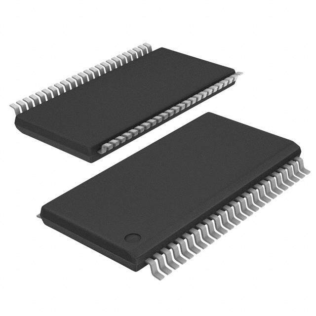
ICGOO电子元器件商城为您提供MC14050BDG由ON Semiconductor设计生产,在icgoo商城现货销售,并且可以通过原厂、代理商等渠道进行代购。 MC14050BDG价格参考¥0.67-¥1.67。ON SemiconductorMC14050BDG封装/规格:逻辑 - 缓冲器,驱动器,接收器,收发器, Buffer, Non-Inverting 6 Element 1 Bit per Element Push-Pull Output 16-SOIC。您可以下载MC14050BDG参考资料、Datasheet数据手册功能说明书,资料中有MC14050BDG 详细功能的应用电路图电压和使用方法及教程。
ON Semiconductor的MC14050BDG是一款六路非反相缓冲器/线路驱动器,属于逻辑缓冲器、驱动器类器件。该芯片广泛应用于需要信号缓冲和驱动能力增强的数字电路中。

其主要应用场景包括:

1. 数字电路信号缓冲:用于增强信号驱动能力,隔离前后级电路,防止负载变化影响信号源稳定性。

2. 接口电路设计:在微处理器、存储器或逻辑电路之间作为接口,提高信号传输的稳定性和可靠性。

3. 显示驱动应用:如用于驱动七段数码管、LED显示器等,提供足够的电流驱动能力。

4. 工业控制系统:适用于工业自动化设备中的信号调理和驱动,提高抗干扰能力和信号完整性。

5. 消费电子产品:如家用电器、仪表显示等场合,用于逻辑信号的缓冲和放大。

该器件采用CMOS工艺,具有低功耗、宽电源电压范围(通常为3V至18V)以及高抗干扰能力等特点,适合多种应用场景。封装形式通常为16引脚SOIC或DIP,便于在不同电路板中使用。
| 参数 | 数值 |
| 产品目录 | 集成电路 (IC)半导体 |
| 描述 | IC BUFFER HEX NON-INVERT 16SOIC缓冲器和线路驱动器 3-18V Hex CMOS Buffer |
| 产品分类 | |
| 品牌 | ON Semiconductor |
| 产品手册 | |
| 产品图片 |
|
| rohs | 符合RoHS无铅 / 符合限制有害物质指令(RoHS)规范要求 |
| 产品系列 | 逻辑集成电路,缓冲器和线路驱动器,ON Semiconductor MC14050BDG4000B |
| 数据手册 | |
| 产品型号 | MC14050BDG |
| 产品目录页面 | |
| 产品种类 | 缓冲器和线路驱动器 |
| 传播延迟时间 | 140 ns at 5 V, 80 ns at 10 V, 60 ns at 15 V |
| 低电平输出电流 | 30 mA |
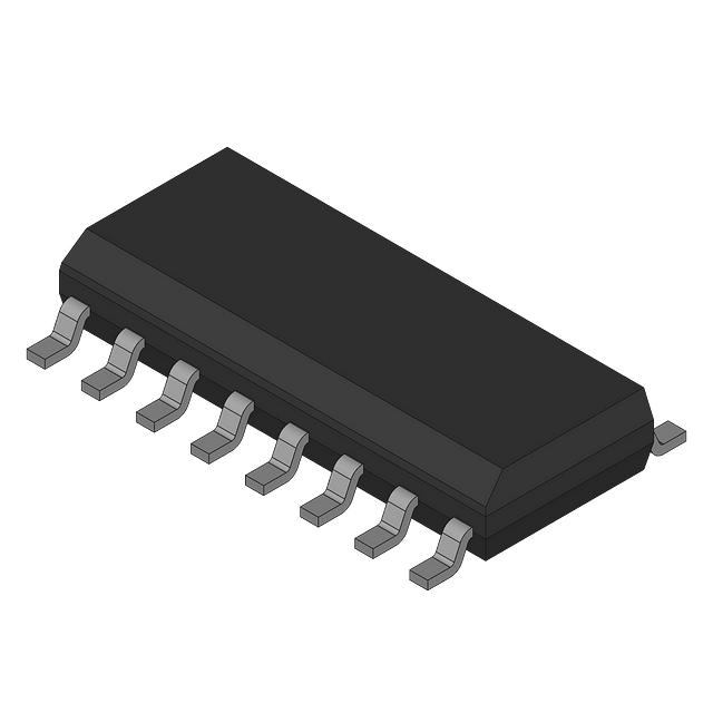
| 供应商器件封装 | 16-SOIC |
| 元件数 | 6 |
| 其它名称 | MC14050BDG-ND |
| 包装 | 管件 |
| 商标 | ON Semiconductor |
| 安装类型 | 表面贴装 |
| 安装风格 | SMD/SMT |
| 封装 | Tube |
| 封装/外壳 | 16-SOIC(0.154",3.90mm 宽) |
| 封装/箱体 | SOIC-16 |
| 工作温度 | -55°C ~ 125°C |
| 工厂包装数量 | 48 |
| 最大工作温度 | + 125 C |
| 最小工作温度 | - 55 C |
| 极性 | Non-Inverting |
| 标准包装 | 48 |
| 每元件位数 | 1 |
| 每芯片的通道数量 | 5 |
| 电压-电源 | 3 V ~ 18 V |
| 电流-输出高,低 | 10mA,40mA |
| 电源电压-最大 | 18 V |
| 电源电压-最小 | 3 V |
| 系列 | MC14050B |
| 输入线路数量 | 6 |
| 输出线路数量 | 6 |
| 逻辑类型 | 缓冲器/线路驱动器,非反相 |
| 逻辑系列 | 4000 |
| 高电平输出电流 | - 4.7 mA |


PDF Datasheet 数据手册内容提取
MC14049B, MC14050B Hex Buffer The MC14049B Hex Inverter/Buffer and MC14050B Noninverting Hex Buffer are constructed with MOS P−Channel and N−Channel enhancement mode devices in a single monolithic structure. These complementary MOS devices find primary use where low power dissipation and/or high noise immunity is desired. These devices http://onsemi.com provide logic level conversion using only one supply voltage, V . DD The input−signal high level (V ) can exceed the V supply IH DD voltage for logic level conversions. Two TTL/DTL loads can be driven when the devices are used as a CMOS−to−TTL/DTL converter (VDD = 5.0 V, VOL ≤ 0.4 V, IOL ≥ 3.2 mA). SOIC−16 SOEIAJ−16 TSSOP−16 Note that pins 13 and 16 are not connected internally on these D SUFFIX F SUFFIX DT SUFFIX devices; consequently connections to these terminals will not affect CASE 751B CASE 966 CASE 948F circuit operation. PIN ASSIGNMENT Features • High Source and Sink Currents • VDD 1 16 NC High−to−Low Level Converter • OUTA 2 15 OUTF Supply Voltage Range = 3.0 V to 18 V • INA 3 14 INF V can exceed V IN DD • Meets JEDEC B Specifications OUTB 4 13 NC • Improved ESD Protection On All Inputs INB 5 12 OUTE • NLV Prefix for Automotive and Other Applications Requiring OUTC 6 11 INE Unique Site and Control Change Requirements; AEC−Q100 INC 7 10 OUTD Qualified and PPAP Capable VSS 8 9 IND • These Devices are Pb−Free and are RoHS Compliant MAXIMUM RATINGS (Voltages Referenced to VSS) MARKING DIAGRAMS Symbol Parameter Value Unit 16 16 VDD DC Supply Voltage Range −0.5 to +18.0 V 140xxBG MC140xxB Vin Input Voltage Range (DC or Transient) −0.5 to +18.0 V AWLYWW ALYWG Vout Output Voltage Range (DC or Transient) −0.5 to VDD + V 1 1 0.5 SOIC−16 SOEIAJ−16 Iin Input Current (DC or Transient) per Pin ±10 mA Iout Output Current (DC or Transient) per Pin ±45 mA 16 14 PD Power Dissipation, per Package (Note 1) mW 050B (Plastic) 825 ALYW(cid:2) (SOIC) 740 (cid:2) TA Ambient Temperature Range −55 to +125 °C 1 Tstg Storage Temperature Range −65 to +150 °C TSSOP−16 TL Lead Temperature (8−Second Soldering) 260 °C xx = Specific Device Code Stresses exceeding those listed in the Maximum Ratings table may damage the A = Assembly Location device. If any of these limits are exceeded, device functionality should not be WL, L = Wafer Lot assumed, damage may occur and reliability may be affected. YY, Y = Year 1. Temperature Derating: See Figure 3. WW, W = Work Week This device contains protection circuitry to protect the inputs against damage G or (cid:2) = Pb−Free Indicator due to high static voltages or electric fields referenced to the VSS pin only. Extra (Note: Microdot may be in either location) precautions must be taken to avoid applications of any voltage higher than the maximum rated voltages to this high−impedance circuit. For proper operation, the ranges VSS ≤ Vin ≤ 18 V and VSS ≤ Vout ≤ VDD are recommended. ORDERING INFORMATION Unused inputs must always be tied to an appropriate logic voltage level See detailed ordering and shipping information in the package (e.g., either VSS or VDD). Unused outputs must be left open. dimensions section on page 2 of this data sheet. © Semiconductor Components Industries, LLC, 2014 1 Publication Order Number: August, 2014 − Rev. 9 MC14049B/D
MC14049B, MC14050B LOGIC DIAGRAM MC14049B MC14050B 3 2 3 2 5 4 5 4 7 6 7 6 9 10 9 10 11 12 11 12 14 15 14 15 NC = PIN 13, 16 NC = PIN 13, 16 VSS = PIN 8 VSS = PIN 8 VDD = PIN 1 VDD = PIN 1 ORDERING INFORMATION Device Package Shipping† MC14049BDG SOIC−16 48 Units / Rail (Pb−Free) MC14049BDR2G SOIC−16 2500 Units / Tape & Reel (Pb−Free) NLV14049BDR2G* SOIC−16 2500 Units / Tape & Reel (Pb−Free) MC14049BFELG SOEIAJ−16 2000 Units / Tape & Reel (Pb−Free) MC14050BDG SOIC−16 48 Units / Rail (Pb−Free) NLV14050BDG* SOIC−16 48 Units / Rail (Pb−Free) MC14050BDR2G SOIC−16 2500 Units / Tape & Reel (Pb−Free) NLV14050BDR2G* SOIC−16 2500 Units / Tape & Reel (Pb−Free) MC14050BDTG TSSOP−16 96 Units / Rail (Pb−Free) NLV14050BDTG* TSSOP−16 96 Units / Rail (Pb−Free) MC14050BDTR2G TSSOP−16 2500 Units / Tape & Reel (Pb−Free) MC14050BFELG SOEIAJ−16 2000 Units / Tape & Reel (Pb−Free) †For information on tape and reel specifications, including part orientation and tape sizes, please refer to our Tape and Reel Packaging Specifications Brochure, BRD8011/D. *NLV Prefix for Automotive and Other Applications Requiring Unique Site and Control Change Requirements; AEC−Q100 Qualified and PPAP Capable. http://onsemi.com 2
MC14049B, MC14050B ELECTRICAL CHARACTERISTICS (Voltages Referenced to VSS) –55(cid:3)C +25(cid:3)C +125(cid:3)C VDD Typ Characteristic Symbol Vdc Min Max Min (Note 2) Max Min Max Unit Output Voltage “0” Level VOL 5.0 − 0.05 − 0 0.05 − 0.05 Vdc Vin = VDD 10 − 0.05 − 0 0.05 − 0.05 15 − 0.05 − 0 0.05 − 0.05 “1” Level VOH 5.0 4.95 − 4.95 5.0 − 4.95 − Vdc Vin = 0 10 9.95 − 9.95 10 − 9.95 − 15 14.95 − 14.95 15 − 14.95 − Input Voltage “0” Level VIL Vdc (VO = 4.5 Vdc) 5.0 − 1.5 − 2.25 1.5 − 1.5 (VO = 9.0 Vdc) 10 − 3.0 − 4.50 3.0 − 3.0 (VO = 13.5 Vdc) 15 − 4.0 − 6.75 4.0 − 4.0 “1” Level VIH Vdc (VO = 0.5 Vdc) 5.0 3.5 − 3.5 2.75 − 3.5 − (VO = 1.0 Vdc) 10 7.0 − 7.0 5.50 − 7.0 − (VO = 1.5 Vdc) 15 11 − 11 8.25 − 11 − Output Drive Current IOH mAdc (VOH = 2.5 Vdc) Source 5.0 –1.6 − –1.25 –2.5 − –1.0 − (VOH = 9.5 Vdc) 10 –1.6 − –1.30 –2.6 − –1.0 − (VOH = 13.5 Vdc) 15 –4.7 − –3.75 –10 − –3.0 − (VOL = 0.4 Vdc) Sink IOL 5.0 3.75 − 3.2 6.0 − 2.6 − mAdc (VOL = 0.5 Vdc) 10 10 − 8.0 16 − 6.6 − (VOL = 1.5 Vdc) 15 30 − 24 40 − 19 − Input Current Iin 15 − ±0.1 − ±0.00001 ±0.1 − ±1.0 (cid:2)Adc Input Capacitance (Vin = 0) Cin − − − − 10 20 − − pF Quiescent Current (Per Package) IDD 5.0 − 1.0 − 0.002 1.0 − 30 (cid:2)Adc 10 − 2.0 − 0.004 2.0 − 60 15 − 4.0 − 0.006 4.0 − 120 Total Supply Current (Notes 3 & 4) IT 5.0 IT = (1.8 (cid:2)A/kHz) f + IDD (cid:2)Adc (Dynamic plus Quiescent, 10 IT = (3.5 (cid:2)A/kHz) f + IDD per package) 15 IT = (5.3 (cid:2)A/kHz) f + IDD (CL = 50 pF on all outputs, all buffers switching Product parametric performance is indicated in the Electrical Characteristics for the listed test conditions, unless otherwise noted. Product performance may not be indicated by the Electrical Characteristics if operated under different conditions. 2. Data labelled “Typ” is not to be used for design purposes but is intended as an indication of the IC’s potential performance. 3. The formulas given are for the typical characteristics only at +25(cid:3)C 4. To calculate total supply current at loads other than 50 pF: IT(CL) = IT(50 pF) + (CL − 50) Vfk Where: IT is in (cid:2)A (per Package), CL in pF, V = (VDD − VSS) in volts, f in kHz is input frequency and k = 0.002. http://onsemi.com 3
MC14049B, MC14050B AC SWITCHING CHARACTERISTICS (Note 5) (CL = 50 pF, TA = + 25(cid:3)C) VDD Typ Characteristic Symbol Vdc Min (Note 6) Max Unit Output Rise Time tTLH ns tTLH = (0.7 ns/pF) CL + 65 ns 5.0 − 100 160 tTLH = (0.25 ns/pF) CL + 37.5 ns 10 − 50 80 tTLH = (0.2 ns/pF) CL + 30 ns 15 − 40 60 Output Fall Time tTHL ns tTHL = (0.2 ns/pF) CL + 30 ns 5.0 − 40 60 tTHL = (0.06 ns/pF) CL + 17 ns 10 − 20 40 tTHL = (0.04 ns/pF) CL + 13 ns 15 − 15 30 Propagation Delay Time tPLH ns tPLH = (0.33 ns/pF) CL + 63.5 ns 5.0 − 80 140 tPLH = (0.19 ns/pF) CL + 30.5 ns 10 − 40 80 tPLH = (0.06 ns/pF) CL + 27 ns 15 − 30 60 Propagation Delay Time tPHL ns tPHL = (0.2 ns/pF) CL + 30 ns 5.0 − 40 80 tPHL = (0.1 ns/pF) CL + 15 ns 10 − 20 40 tPHL = (0.05 ns/pF) CL + 12.5 ns 15 − 15 30 5. The formulas given are for the typical characteristics only at 25(cid:3)C. 6. Data labeled “Typ” is not to be used for design purposes but is intended as an indication of the IC’s potential performance. MC14049B MC14050B MC14049B MC14050B VDD VDD VDD VDD 1 1 1 1 IOH IOL IOL IOH VOH VOL VOL VOH 8 VSS 8 VSS 8 VSS 8 VSS VDS = VOH - VDD VDD = VOL 0 160 mAdc) VGS = 5.0 Vdc Adc) VGS = 15 Vdc NT ( -(cid:2)10 T (m120 R N R E U R C -(cid:2)20 R RCE K CU 80 VGS = 10 Vdc U N T SO -(cid:2)30 VGS = 10 Vdc UT SI U P MAXIMUM CURRENT LEVEL P T UT OU 40 , OH-(cid:2)40 VGS = 15 Vdc MAXIMUM CURRENT LEVEL , OL VGS = 5.0 Vdc O I I -(cid:2)50 0 -(cid:2)10 -(cid:2)8.0 -(cid:2)6.0 -(cid:2)4.0 -(cid:2)2.0 0 0 2.0 4.0 6.0 8.0 10 VDS, DRAIN-TO-SOURCE VOLTAGE (Vdc) VDS, DRAIN-TO-SOURCE VOLTAGE (Vdc) Figure 1. Typical Output Source Characteristics Figure 2. Typical Output Sink Characteristics http://onsemi.com 4
MC14049B, MC14050B 1200 W) m 1100 N ( 1000 O TI 900 A P 825 DISSIAGE 877040000 WER PACK 600 UM POPER 540000 (P) PDIP M XI 300 (D) SOIC A P, MD 210000 117250 mmWW ((PD)) 0 25 50 75 100 125 150 175 TA, AMBIENT TEMPERATURE (°C) Figure 3. Ambient Temperature Power Derating 20 ns 20 ns INPUT 90% VDD 50% VDD 10% VSS 1 tPHL tPLH # 90% VOH OUTPUT PULSE MC14049B 50% GENERATOR Vin Vout 10% VOL tPLH tTHL tTLH 8 VSS CL tPHL tPHL OUTPUT 90% VOH 50% MC14050B #(cid:2)Invert on MC14049B only 10% VOL tTLH tTHL Figure 4. Switching Time Test Circuit and Waveforms http://onsemi.com 5
MC14049B, MC14050B PACKAGE DIMENSIONS SOIC−16 D SUFFIX CASE 751B−05 ISSUE K −A− NOTES: 1. DIMENSIONING AND TOLERANCING PER ANSI Y14.5M, 1982. 2. CONTROLLING DIMENSION: MILLIMETER. 16 9 3. DIMENSIONS A AND B DO NOT INCLUDE MOLD PROTRUSION. 4. MAXIMUM MOLD PROTRUSION 0.15 (0.006) PER SIDE. −B− P8 PL 5. DIMENSION D DOES NOT INCLUDE DAMBAR PROTRUSION. ALLOWABLE DAMBAR PROTRUSION 1 8 0.25 (0.010) M B S SHALL BE 0.127 (0.005) TOTAL IN EXCESS OF THE D DIMENSION AT MAXIMUM MATERIAL CONDITION. MILLIMETERS INCHES DIM MIN MAX MIN MAX G A 9.80 10.00 0.386 0.393 B 3.80 4.00 0.150 0.157 C 1.35 1.75 0.054 0.068 F D 0.35 0.49 0.014 0.019 K R X 45(cid:3) F 0.40 1.25 0.016 0.049 G 1.27 BSC 0.050 BSC J 0.19 0.25 0.008 0.009 C K 0.10 0.25 0.004 0.009 M 0 (cid:3) 7 (cid:3) 0 (cid:3) 7 (cid:3) −T− SEATING P 5.80 6.20 0.229 0.244 PLANE M J R 0.25 0.50 0.010 0.019 D 16 PL 0.25 (0.010) M T B S A S SOLDERING FOOTPRINT* 8X 6.40 16X1.12 1 16 16X 0.58 1.27 PITCH 8 9 DIMENSIONS: MILLIMETERS *For additional information on our Pb−Free strategy and soldering details, please download the ON Semiconductor Soldering and Mounting Techniques Reference Manual, SOLDERRM/D. http://onsemi.com 6
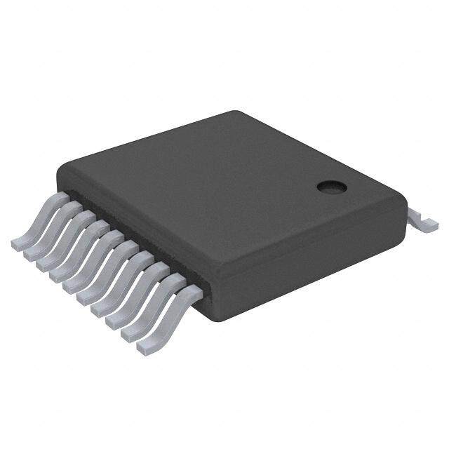
MC14049B, MC14050B PACKAGE DIMENSIONS TSSOP−16 DT SUFFIX CASE 948F ISSUE B 16X K REF NOTES: 0.10 (0.004) M T U S V S 1. DIMENSIONING AND TOLERANCING PER ANSI Y14.5M, 1982. 0.15 (0.006) T U S K 2. CONTROLLING DIMENSION: MILLIMETER. 3. DIMENSION A DOES NOT INCLUDE MOLD ÇÉÇÉK1ÇÉ FLASH. PROTRUSIONS OR GATE BURRS. MOLD FLASH OR GATE BURRS SHALL NOT 16 9 ÇÉÇÉÇÉ EXCEED 0.15 (0.006) PER SIDE. 2XL/2 J1 4. DIMENSION B DOES NOT INCLUDE INTERLEAD FLASH OR PROTRUSION. ÇÇÇ INTERLEAD FLASH OR PROTRUSION SHALL B SECTION N−N NOT EXCEED 0.25 (0.010) PER SIDE. L −U− J 5D.ADMIMBAERN SPIROONT KR UDSOIEOSN N. AOLTL OINWCALUBLDEE DAMBAR PROTRUSION SHALL BE 0.08 PIN 1 (0.003) TOTAL IN EXCESS OF THE K IDENT. N DIMENSION AT MAXIMUM MATERIAL 1 8 0.25 (0.010) CONDITION. 6. TERMINAL NUMBERS ARE SHOWN FOR REFERENCE ONLY. M 7. DIMENSION A AND B ARE TO BE 0.15 (0.006) T U S DETERMINED AT DATUM PLANE −W−. A N MILLIMETERS INCHES −V− DIM MIN MAX MIN MAX F A 4.90 5.10 0.193 0.200 B 4.30 4.50 0.169 0.177 DETAIL E C −−− 1.20 −−− 0.047 D 0.05 0.15 0.002 0.006 F 0.50 0.75 0.020 0.030 G 0.65 BSC 0.026 BSC C −W− H 0.18 0.28 0.007 0.011 J 0.09 0.20 0.004 0.008 J1 0.09 0.16 0.004 0.006 0.10 (0.004) K 0.19 0.30 0.007 0.012 −T− SEATING H DETAIL E K1 0.19 0.25 0.007 0.010 PLANE D G ML 06 .(cid:3) 4 0 BSC8 (cid:3) 00. 2(cid:3) 52 BS8C (cid:3) SOLDERING FOOTPRINT* 7.06 1 0.65 PITCH 16X 16X 0.36 1.26 DIMENSIONS: MILLIMETERS *For additional information on our Pb−Free strategy and soldering details, please download the ON Semiconductor Soldering and Mounting Techniques Reference Manual, SOLDERRM/D. http://onsemi.com 7
MC14049B, MC14050B PACKAGE DIMENSIONS SOEIAJ−16 F SUFFIX CASE 966 ISSUE A NOTES: 16 9 LE (cid:3)(cid:4)1. DIMENSIONING AND TOLERANCING PER ANSI Y14.5M, 1982. Q1 (cid:3)(cid:4)2. CONTROLLING DIMENSION: MILLIMETER. (cid:3)(cid:4)3. DIMENSIONS D AND E DO NOT INCLUDE E HE M(cid:3) MOLD FLASH OR PROTRUSIONS AND ARE MEASURED AT THE PARTING LINE. MOLD FLASH OR PROTRUSIONS SHALL NOT EXCEED 0.15 (0.006) PER SIDE. 1 8 L (cid:3)(cid:4)4. TERMINAL NUMBERS ARE SHOWN FOR REFERENCE ONLY. DETAIL P (cid:3)(cid:4)5. THE LEAD WIDTH DIMENSION (b) DOES NOT Z INCLUDE DAMBAR PROTRUSION. ALLOWABLE DAMBAR PROTRUSION SHALL BE 0.08 (0.003) D TOTAL IN EXCESS OF THE LEAD WIDTH DIMENSION AT MAXIMUM MATERIAL CONDITION. VIEW P DAMBAR CANNOT BE LOCATED ON THE LOWER e A RADIUS OR THE FOOT. MINIMUM SPACE c BETWEEN PROTRUSIONS AND ADJACENT LEAD TO BE 0.46 ( 0.018). MILLIMETERS INCHES DIM MIN MAX MIN MAX A --- 2.05 --- 0.081 b A1 A1 0.05 0.20 0.002 0.008 b 0.35 0.50 0.014 0.020 0.13 (0.005) M 0.10 (0.004) Dc 09..1900 100..5200 00..030970 00..401131 E 5.10 5.45 0.201 0.215 e 1.27 BSC 0.050 BSC HE 7.40 8.20 0.291 0.323 L 0.50 0.85 0.020 0.033 LE 1.10 1.50 0.043 0.059 M 0 (cid:3) 10 (cid:3) 0 (cid:3) 10 (cid:3) Q1 0.70 0.90 0.028 0.035 Z --- 0.78 --- 0.031 ON Semiconductor and the are registered trademarks of Semiconductor Components Industries, LLC (SCILLC) or its subsidiaries in the United States and/or other countries. SCILLC owns the rights to a number of patents, trademarks, copyrights, trade secrets, and other intellectual property. A listing of SCILLC’s product/patent coverage may be accessed at www.onsemi.com/site/pdf/Patent−Marking.pdf. SCILLC reserves the right to make changes without further notice to any products herein. SCILLC makes no warranty, representation or guarantee regarding the suitability of its products for any particular purpose, nor does SCILLC assume any liability arising out of the application or use of any product or circuit, and specifically disclaims any and all liability, including without limitation special, consequential or incidental damages. “Typical” parameters which may be provided in SCILLC data sheets and/or specifications can and do vary in different applications and actual performance may vary over time. All operating parameters, including “Typicals” must be validated for each customer application by customer’s technical experts. SCILLC does not convey any license under its patent rights nor the rights of others. SCILLC products are not designed, intended, or authorized for use as components in systems intended for surgical implant into the body, or other applications intended to support or sustain life, or for any other application in which the failure of the SCILLC product could create a situation where personal injury or death may occur. Should Buyer purchase or use SCILLC products for any such unintended or unauthorized application, Buyer shall indemnify and hold SCILLC and its officers, employees, subsidiaries, affiliates, and distributors harmless against all claims, costs, damages, and expenses, and reasonable attorney fees arising out of, directly or indirectly, any claim of personal injury or death associated with such unintended or unauthorized use, even if such claim alleges that SCILLC was negligent regarding the design or manufacture of the part. SCILLC is an Equal Opportunity/Affirmative Action Employer. This literature is subject to all applicable copyright laws and is not for resale in any manner. PUBLICATION ORDERING INFORMATION LITERATURE FULFILLMENT: N. American Technical Support: 800−282−9855 Toll Free ON Semiconductor Website: www.onsemi.com Literature Distribution Center for ON Semiconductor USA/Canada P.O. Box 5163, Denver, Colorado 80217 USA Europe, Middle East and Africa Technical Support: Order Literature: http://www.onsemi.com/orderlit Phone: 303−675−2175 or 800−344−3860 Toll Free USA/Canada Phone: 421 33 790 2910 Fax: 303−675−2176 or 800−344−3867 Toll Free USA/Canada Japan Customer Focus Center For additional information, please contact your local Email: orderlit@onsemi.com Phone: 81−3−5817−1050 Sales Representative http://onsemi.com MC14049B/D 8
Mouser Electronics Authorized Distributor Click to View Pricing, Inventory, Delivery & Lifecycle Information: O N Semiconductor: MC14049BDG MC14049BDR2G MC14050BDG MC14050BDR2G MC14050BDTG MC14050BDTR2G