 Datasheet下载
- 型号: MC14043BDG
- 制造商: ON Semiconductor
- 库位|库存: xxxx|xxxx
- 要求:
| 数量阶梯 | 香港交货 | 国内含税 |
| +xxxx | $xxxx | ¥xxxx |
查看当月历史价格
查看今年历史价格
MC14043BDG产品简介:
ICGOO电子元器件商城为您提供MC14043BDG由ON Semiconductor设计生产,在icgoo商城现货销售,并且可以通过原厂、代理商等渠道进行代购。 MC14043BDG价格参考¥1.76-¥5.44。ON SemiconductorMC14043BDG封装/规格:逻辑 - 锁销, S-R Latch 4 Channel 1:1 IC Tri-State 16-SOIC。您可以下载MC14043BDG参考资料、Datasheet数据手册功能说明书,资料中有MC14043BDG 详细功能的应用电路图电压和使用方法及教程。
ON Semiconductor的MC14043BDG属于逻辑电路中的锁存器(Latches)类别,具体来说是一种双四输入与非门(Dual 4-Input NAND Gate)。这种器件在数字电子系统中广泛应用,主要用于信号处理、数据存储和控制逻辑等方面。以下是其主要应用场景:

 1. 组合逻辑设计
MC14043BDG可以用于构建复杂的组合逻辑电路。通过多个与非门的组合,可以实现各种逻辑功能,如加法器、减法器、比较器等。这种灵活性使得它在许多数字系统中成为基础元件。

 2. 脉冲信号处理
该芯片常用于脉冲信号的处理和整形。例如,在时钟电路或同步电路中,它可以用来生成精确的脉冲信号,确保系统的时序一致性。此外,它还可以用于脉冲展宽、脉冲压缩等操作,以适应不同的应用需求。

 3. 存储和记忆功能
作为锁存器的一种,MC14043BDG可以在某些情况下用作简单的存储单元。例如,在需要临时保存状态信息的场景中,它可以用来保持某个逻辑电平,直到下一个触发信号到来。这种特性在一些自动控制系统中非常有用。

 4. 驱动和接口电路
MC14043BDG还可以用作驱动电路的一部分,尤其是在需要增强信号驱动能力的情况下。它可以与其他逻辑门配合使用,形成更强大的驱动电路,适用于驱动LED、继电器等负载。

 5. 编码和解码
在编码和解码电路中,MC14043BDG可以用来实现多路选择或多路复用功能。例如,在地址译码器或数据选择器中,它可以用来根据输入信号选择特定的输出通道。

 6. 通信和网络设备
在通信和网络设备中,MC14043BDG可以用于信号的检测和处理。例如,在串行通信接口中,它可以用来检测起始位和停止位,确保数据的正确传输。

 7. 消费电子产品
在消费电子产品中,如电视、音响等,MC14043BDG可以用于控制面板的逻辑处理,帮助实现各种功能按钮的操作逻辑。

总之,MC14043BDG作为一种基本的逻辑元件,具有广泛的应用前景,尤其适合于需要精确逻辑控制和信号处理的场合。
| 参数 | 数值 |
| 产品目录 | 集成电路 (IC)半导体 |
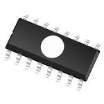
| 描述 | IC LATCH R-S QUAD NOR 16SOIC闭锁 3-18V Quad R-S |
| 产品分类 | |
| 品牌 | ON Semiconductor |
| 产品手册 | |
| 产品图片 |
|
| rohs | 符合RoHS无铅 / 符合限制有害物质指令(RoHS)规范要求 |
| 产品系列 | 逻辑集成电路,闭锁,ON Semiconductor MC14043BDG4000B |
| 数据手册 | |
| 产品型号 | MC14043BDG |
| 产品目录页面 | |
| 产品种类 | 闭锁 |
| 传播延迟时间 | 350 ns at 5 V, 175 ns at 10 V, 120 ns at 15 V |
| 低电平输出电流 | 32 mA |
| 供应商器件封装 | 16-SOIC |
| 其它名称 | MC14043BDGOS |
| 包装 | 管件 |
| 商标 | ON Semiconductor |
| 安装类型 | 表面贴装 |
| 安装风格 | SMD/SMT |
| 封装 | Tube |
| 封装/外壳 | 16-SOIC(0.154",3.90mm 宽) |
| 封装/箱体 | SOIC-16 |
| 工作温度 | -55°C ~ 125°C |
| 工厂包装数量 | 48 |
| 延迟时间-传播 | 60ns |
| 最大工作温度 | + 125 C |
| 最小工作温度 | - 55 C |
| 极性 | Non-Inverting |
| 标准包装 | 48 |
| 独立电路 | 4 |
| 电压-电源 | 3 V ~ 18 V |
| 电流-输出高,低 | 8.8mA,8.8mA |
| 电源电压-最大 | 18 V |
| 电源电压-最小 | 3 V |
| 电路 | 1:1 |
| 电路数量 | 4 Circuit |
| 系列 | MC14043B |
| 输入线路数量 | 8 Line |
| 输出类型 | 三态 |
| 输出线路数量 | 4 Line |
| 逻辑类型 | S-R Latch |
| 逻辑系列 | MC14 |
| 高电平输出电流 | - 4.2 mA |


- 商务部:美国ITC正式对集成电路等产品启动337调查
- 曝三星4nm工艺存在良率问题 高通将骁龙8 Gen1或转产台积电
- 太阳诱电将投资9.5亿元在常州建新厂生产MLCC 预计2023年完工
- 英特尔发布欧洲新工厂建设计划 深化IDM 2.0 战略
- 台积电先进制程称霸业界 有大客户加持明年业绩稳了
- 达到5530亿美元!SIA预计今年全球半导体销售额将创下新高
- 英特尔拟将自动驾驶子公司Mobileye上市 估值或超500亿美元
- 三星加码芯片和SET,合并消费电子和移动部门,撤换高东真等 CEO
- 三星电子宣布重大人事变动 还合并消费电子和移动部门
- 海关总署:前11个月进口集成电路产品价值2.52万亿元 增长14.8%


PDF Datasheet 数据手册内容提取
MC14043B, MC14044B CMOS MSI Quad R−S Latches The MC14043B and MC14044B quad R−S latches are constructed with MOS P−Channel and N−Channel enhancement mode devices in asingle monolithic structure. Each latch has an independent Q output http://onsemi.com and set and reset inputs. The Q outputs are gated through three−state buffers having a common enable input. The outputs are enabled with alogical “1” or high on the enable input; a logical “0” or low disconnects the latch from the Q outputs, resulting in an open circuit at the Q outputs. SOIC−16 SOEIAJ−16 D SUFFIX F SUFFIX Features CASE 751B CASE 966 • Double Diode Input Protection • MARKING DIAGRAMS Three−State Outputs with Common Enable • Outputs Capable of Driving Two Low−power TTL Loads or One 16 Low−Power Schottky TTL Load Over the Rated Temperature Range 140xxBG • AWLYWW Supply Voltage Range = 3.0 Vdc to 18 Vdc • NLV Prefix for Automotive and Other Applications Requiring 1 Unique Site and Control Change Requirements; AEC−Q100 SOIC−16 Qualified and PPAP Capable • These Devices are Pb−Free and are RoHS Compliant 16 MC14043B MAXIMUM RATINGS (Voltages Referenced to VSS) ALYWG Symbol Parameter Value Unit 1 VDD DC Supply Voltage Range −0.5 to +18.0 V SOEIAJ−16 Vin, Vout Input or Output Voltage Range −0.5 to VDD + 0.5 V (DC or Transient) xx = Specific Device Code Iin, Iout Input or Output Current ±10 mA A = Assembly Location (DC or Transient) per Pin WL, L = Wafer Lot YY, Y = Year PD Power Dissipation, per Package 500 mW WW, W = Work Week (Note 1) G = Pb−Free Indicator TA Ambient Temperature Range −55 to +125 °C Tstg Storage Temperature Range −65 to +150 °C ORDERING INFORMATION See detailed ordering and shipping information in the package TL Lead Temperature 260 °C dimensions section on page 5 of this data sheet. (8−Second Soldering) Stresses exceeding those listed in the Maximum Ratings table may damage the device. If any of these limits are exceeded, device functionality should not be assumed, damage may occur and reliability may be affected. 1. Temperature Derating: “D/DW” Packages: –7.0 mW/(cid:2)C From 65(cid:2)C To 125(cid:2)C This device contains protection circuitry to guard against damage due to high static voltages or electric fields. However, precautions must be taken to avoid applications of any voltage higher than maximum rated voltages to this high−impedance circuit. For proper operation, Vin and Vout should be constrained to the range VSS ≤ (Vin or Vout) ≤ VDD. Unused inputs must always be tied to an appropriate logic voltage level (e.g., either VSS or VDD). Unused outputs must be left open. © Semiconductor Components Industries, LLC, 2014 1 Publication Order Number: August, 2014 − Rev. 10 MC14043B/D
MC14043B, MC14044B PIN ASSIGNMENT MC14043B MC14044B Q3 1 16 VDD Q3 1 16 VDD Q0 2 15 R3 NC 2 15 S3 R0 3 14 S3 S0 3 14 R3 S0 4 13 NC R0 4 13 Q0 E 5 12 S2 E 5 12 R2 S1 6 11 R2 R1 6 11 S2 R1 7 10 Q2 S1 7 10 Q2 VSS 8 9 Q1 VSS 8 9 Q1 NC = NO CONNECTION MC14043B MC14044B 4 4 S0 2 R0 13 Q0 Q0 3 3 R0 S0 6 6 S1 9 R1 9 Q1 Q1 R1 7 VDD = PIN 16 S1 7 VDD = PIN 16 VSS = PIN 8 VSS = PIN 8 12 NC = PIN 13 12 NC = PIN 2 S2 10 R2 10 Q2 Q2 11 11 R2 S2 14 14 S3 1 TRUTH TABLE R3 1 TRUTH TABLE Q3 Q3 S R E Q S R E Q X X 0 High X X 0 High Impedance Impedance 15 15 R3 0 0 1 No Change S3 0 0 1 0 0 1 1 0 0 1 1 1 5 1 0 1 1 5 1 0 1 0 1 1 1 1 1 1 1 No Change ENABLE ENABLE X = Don’t Care X = Don’t Care http://onsemi.com 2
MC14043B, MC14044B ELECTRICAL CHARACTERISTICS (Voltages Referenced to VSS) − 55(cid:2)C 25(cid:2)C 125(cid:2)C VDD Typ Characteristic Symbol Vdc Min Max Min (Note 2) Max Min Max Unit Output Voltage “0” Level VOL 5.0 − 0.05 − 0 0.05 − 0.05 Vdc Vin = VDD or 0 10 − 0.05 − 0 0.05 − 0.05 15 − 0.05 − 0 0.05 − 0.05 “1” Level VOH 5.0 4.95 − 4.95 5.0 − 4.95 − Vdc Vin = 0 or VDD 10 9.95 − 9.95 10 − 9.95 − 15 14.95 − 14.95 15 − 14.95 − Input Voltage “0” Level VIL Vdc (VO = 4.5 or 0.5 Vdc) 5.0 − 1.5 − 2.25 1.5 − 1.5 (VO = 9.0 or 1.0 Vdc) 10 − 3.0 − 4.50 3.0 − 3.0 (VO = 13.5 or 1.5 Vdc) 15 − 4.0 − 6.75 4.0 − 4.0 “1” Level VIH Vdc (VO = 0.5 or 4.5 Vdc) 5.0 3.5 − 3.5 2.75 − 3.5 − (VO = 1.0 or 9.0 Vdc) 10 7.0 − 7.0 5.50 − 7.0 − (VO = 1.5 or 13.5 Vdc) 15 11 − 11 8.25 − 11 − Output Drive Current IOH mAdc (VOH = 2.5 Vdc) Source 5.0 –3.0 − –2.4 –4.2 − –1.7 − (VOH = 4.6 Vdc) 5.0 –0.64 − –0.51 –0.88 − –0.36 − (VOH = 9.5 Vdc) 10 –1.6 − –1.3 –2.25 − –0.9 − (VOH = 13.5 Vdc) 15 –4.2 − –3.4 –8.8 − –2.4 − (VOL = 0.4 Vdc) Sink IOL 5.0 0.64 − 0.51 0.88 − 0.36 − mAdc (VOL = 0.5 Vdc) 10 1.6 − 1.3 2.25 − 0.9 − (VOL = 1.5 Vdc) 15 4.2 − 3.4 8.8 − 2.4 − Input Current Iin 15 − ±0.1 − ±0.00001 ±0.1 − ±1.0 (cid:2)Adc Input Capacitance Cin − − − − 5.0 7.5 − − pF (Vin = 0) Quiescent Current IDD 5.0 − 1.0 − 0.002 1.0 − 30 (cid:2)Adc (Per Package) 10 − 2.0 − 0.004 2.0 − 60 15 − 4.0 − 0.006 4.0 − 120 Total Supply Current (Notes 3 & 4) IT 5.0 IT = (0.58 (cid:2)A/kHz) f + IDD (cid:2)Adc (Dynamic plus Quiescent, 10 IT = (1.15 (cid:2)A/kHz) f + IDD Per Package) 15 IT = (1.73 (cid:2)A/kHz) f + IDD (CL = 50 pF on all outputs all buffers switching) Three−State Output Leakage ITL 15 − ±0.1 − ±0.0001 ±0.1 − ±3.0 (cid:2)Adc Current Product parametric performance is indicated in the Electrical Characteristics for the listed test conditions, unless otherwise noted. Product performance may not be indicated by the Electrical Characteristics if operated under different conditions. 2. Data labelled “Typ” is not to be used for design purposes but is intended as an indication of the IC’s potential performance. 3. The formulas given are for the typical characteristics only at 25(cid:2)C. 4. To calculate total supply current at loads other than 50 pF: IT(CL) = IT(50 pF) + (CL − 50) Vfk where: IT is in (cid:2)A (per package), CL in pF, V = (VDD − VSS) in volts, f in kHz is input frequency, and k = 0.004. http://onsemi.com 3
MC14043B, MC14044B ÎÎÎÎÎÎÎÎÎÎÎÎÎÎÎÎÎÎÎÎÎÎÎÎÎÎÎÎÎÎÎÎÎ SWITCHING CHARACTERISTICS (Note 5) (CL = 50 pF, TA = 25(cid:2)C) ÎÎÎÎÎÎÎÎÎÎÎÎÎÎÎÎÎÎÎÎÎÎÎÎÎÎÎÎÎÎÎÎÎÎÎÎÎÎÎÎÎÎÎÎÎÎÎÎÎÎÎÎÎÎÎÎÎÎÎÎÎÎÎÎÎÎÎÎÎÎÎÎ VDD Typ ÎÎÎÎÎÎÎÎÎÎÎÎCÎÎharÎÎacteÎÎristiÎÎc ÎÎÎÎÎÎÎÎÎÎÎÎÎÎSyÎÎmboÎÎl ÎÎÎÎÎÎVdÎÎc ÎÎÎÎÎÎMiÎÎn ÎÎÎÎÎÎ(NotÎÎe 6)ÎÎÎÎÎÎMÎÎax ÎÎÎÎÎÎUnÎÎit ÎÎOutpÎut RÎise ÎTimeÎÎÎÎÎÎÎÎÎÎÎÎtÎTLHÎÎÎÎÎÎÎÎÎÎÎÎÎÎÎÎÎÎÎÎnsÎ ÎÎtÎTLH Î= (1.Î35 nÎs/pFÎ) CLÎ + 32Î.5 nÎs ÎÎÎÎÎÎÎÎÎÎÎÎ5.0ÎÎÎÎ−ÎÎÎÎ10Î0 ÎÎÎ2Î00 ÎÎÎÎ tTLH = (0.60 ns/pF) CL + 20 ns 10 − 50 100 ÎÎÎÎtÎÎTLH ÎÎ= (0.ÎÎ40 nÎÎs/pFÎÎ) CLÎÎ + 20ÎÎ nsÎÎÎÎÎÎÎÎÎÎÎÎÎÎÎÎÎÎÎÎÎÎÎÎÎÎ15ÎÎÎÎÎÎÎÎ−ÎÎÎÎÎÎÎÎ4ÎÎ0 ÎÎÎÎÎÎ8ÎÎ0 ÎÎÎÎÎÎÎÎ ÎÎOutpÎut FÎall TÎimeÎÎÎÎÎÎÎÎÎÎÎÎtÎTHLÎÎÎÎÎÎÎÎÎÎÎÎÎÎÎÎÎÎÎÎnsÎ tTHL = (1.35 ns/pF) CL + 32.5 ns 5.0 − 100 200 ÎÎtÎTHL Î= (0.Î60 nÎs/pFÎ) CLÎ + 20Î nsÎÎÎÎÎÎÎÎÎÎÎÎÎ10ÎÎÎÎ−ÎÎÎÎ5Î0 ÎÎÎ1Î00 ÎÎÎÎ ÎÎÎÎtÎÎTHL ÎÎ= (0.ÎÎ40 nÎÎs/pFÎÎ) CLÎÎ + 20ÎÎ nsÎÎÎÎÎÎÎÎÎÎÎÎÎÎÎÎÎÎÎÎÎÎÎÎÎÎ15ÎÎÎÎÎÎÎÎ−ÎÎÎÎÎÎÎÎ4ÎÎ0 ÎÎÎÎÎÎ8ÎÎ0 ÎÎÎÎÎÎÎÎ Propagation Delay Time tPLH ns ÎÎÎÎÎÎÎÎÎÎÎÎÎÎÎÎÎÎÎÎÎÎÎÎÎÎÎÎÎÎÎÎÎÎÎÎÎÎÎ tPLH = (0.90 ns/pF) CL + 130 ns 5.0 − 175 350 ÎÎtÎPLH Î= (0.Î36 nÎs/pFÎ) CLÎ + 57Î nsÎÎÎÎÎÎÎÎÎÎÎÎÎ10ÎÎÎÎ−ÎÎÎÎ7Î5 ÎÎÎ1Î75 ÎÎÎÎ tPLH = (0.26 ns/pF) CL + 47 ns 15 − 60 120 ÎÎÎÎÎÎÎÎÎÎÎÎÎÎÎÎÎÎÎÎÎÎÎÎÎÎÎÎÎÎÎÎÎÎÎÎÎÎÎÎÎÎÎÎÎÎÎÎÎÎÎÎÎÎÎÎÎÎÎÎÎÎÎÎÎÎÎÎÎÎÎÎÎÎÎÎÎÎ tPHL = (0.90 ns/pF) CL + 130 ns tPHL 5.0 − 175 350 ns ÎÎtÎPHL Î= (0.Î90 nÎs/pFÎ) CLÎ + 57Î nsÎÎÎÎÎÎÎÎÎÎÎÎÎ10ÎÎÎÎ−ÎÎÎÎ7Î5 ÎÎÎ1Î75 ÎÎÎÎ ÎÎÎÎtÎÎPHL ÎÎ= (0.ÎÎ26 nÎÎs/pFÎÎ) CLÎÎ + 47ÎÎ nsÎÎÎÎÎÎÎÎÎÎÎÎÎÎÎÎÎÎÎÎÎÎÎÎÎÎ15ÎÎÎÎÎÎÎÎ−ÎÎÎÎÎÎÎÎ6ÎÎ0 ÎÎÎÎÎÎ1ÎÎ20 ÎÎÎÎÎÎÎÎ Set, Set Pulse Width tW 5.0 200 80 − ns ÎÎÎÎÎÎÎÎÎÎÎÎÎÎÎÎÎÎÎÎÎÎ10ÎÎÎÎ10Î0 ÎÎÎ4Î0 ÎÎÎÎ− ÎÎÎÎ ÎÎÎÎÎÎÎÎÎÎÎÎÎÎÎÎÎÎÎÎÎÎÎÎÎÎÎÎÎÎÎÎÎÎÎÎÎÎÎÎÎÎÎÎ15ÎÎÎÎÎÎÎÎ70ÎÎÎÎÎÎÎÎ3ÎÎ0 ÎÎÎÎÎÎÎÎ− ÎÎÎÎÎÎÎÎ ÎÎResÎet, RÎeseÎt PulÎse WÎidthÎÎÎÎÎÎÎÎÎÎÎtW ÎÎÎÎ5.0ÎÎÎÎ20Î0 ÎÎÎ8Î0 ÎÎÎÎ− ÎÎÎnsÎ 10 100 40 − ÎÎÎÎÎÎÎÎÎÎÎÎÎÎÎÎÎÎÎÎÎÎÎÎÎÎÎÎÎÎÎÎÎÎÎÎÎÎÎÎÎÎÎÎ15ÎÎÎÎÎÎÎÎ70ÎÎÎÎÎÎÎÎ3ÎÎ0 ÎÎÎÎÎÎÎÎ− ÎÎÎÎÎÎÎÎ ÎÎThreÎe−SÎtateÎ EnaÎble/DÎisabÎle DÎelayÎÎÎÎÎÎÎÎtPÎLZ,ÎÎÎÎ5.0ÎÎÎÎ−ÎÎÎÎ15Î0 ÎÎÎ3Î00 ÎÎÎnsÎ tPHZ, 10 − 80 160 ÎÎÎÎÎÎÎÎÎÎÎÎÎÎÎÎÎtPÎZL,ÎÎÎÎ15ÎÎÎÎ−ÎÎÎÎ5Î5 ÎÎÎ1Î10 ÎÎÎÎ ÎÎÎÎÎÎÎÎÎÎÎÎÎÎÎÎÎtÎPZHÎÎÎÎÎÎÎÎÎÎÎÎÎÎÎÎÎÎÎÎÎ 5. The formulas given are for the typical characteristics only at 25(cid:2)C. 6. Data labelled “Typ” is not to be used for design purposes but is intended as an indication of the IC’s potential performance. AC WAVEFORMS MC14043B MC14044B 20 ns 20 ns 20 ns 20 ns 90% VDD 90% VDD 50% 50% SET 10% VSS SET 10% VSS 20 ns 20 ns 20 ns 20 ns 90% VDD 90% VDD 50% 50% RESET 10% VSS RESET 10% VSS tTHL 90%tTLH VOH tTLH 90% tTHL VOH Q 10% 50% VOL Q 50% 10% VOL tPHL tPLH tPLH tPHL http://onsemi.com 4
MC14043B, MC14044B THREE−STATE ENABLE/DISABLE DELAYS Set, Reset, Enable, and Switch Conditions for 3−State Tests VDD MC14043B MC14044B Test Enable S1 S2 Q S R S R S1 tPZH Open Closed A VDD VSS VSS VDD TO tPZL Closed Open B VSS VDD VDD VSS 1 k OUTPUT tPHZ Open Closed A VDD VSS VSS VDD UNDER CL TEST tPLZ Closed Open B VSS VDD VDD VSS 50 pF S2 VSS VDD ENABLE 50% VSS tPZH VDD 90% QA 10% tPHZ VOL tPZL tPLZ VOH QB 10% VSS ORDERING INFORMATION Device Package Shipping† MC14043BDG SOIC−16 48 Units / Rail (Pb−Free) NLV14043BDG* SOIC−16 48 Units / Rail (Pb−Free) MC14043BDR2G SOIC−16 2500 Units / Tape & Reel (Pb−Free) NLV14043BDR2G* SOIC−16 2500 Units / Tape & Reel (Pb−Free) MC14043BFELG SOEIAJ−16 2000 Units / Tape & Reel (Pb−Free) MC14044BDG SOIC−16 48 Units / Rail (Pb−Free) NLV14044BDG* SOIC−16 48 Units / Rail (Pb−Free) MC14044BDR2G SOIC−16 2500 Units / Tape & Reel (Pb−Free) NLV14044BDR2G* SOIC−16 2500 Units / Tape & Reel (Pb−Free) †For information on tape and reel specifications, including part orientation and tape sizes, please refer to our Tape and Reel Packaging Specifications Brochure, BRD8011/D. *NLV Prefix for Automotive and Other Applications Requiring Unique Site and Control Change Requirements; AEC−Q100 Qualified and PPAP Capable. http://onsemi.com 5
MC14043B, MC14044B PACKAGE DIMENSIONS SOIC−16 D SUFFIX CASE 751B−05 ISSUE K −A− NOTES: 1. DIMENSIONING AND TOLERANCING PER ANSI Y14.5M, 1982. 2. CONTROLLING DIMENSION: MILLIMETER. 16 9 3. DIMENSIONS A AND B DO NOT INCLUDE MOLD PROTRUSION. 4. MAXIMUM MOLD PROTRUSION 0.15 (0.006) PER SIDE. −B− P8 PL 5. DIMENSION D DOES NOT INCLUDE DAMBAR PROTRUSION. ALLOWABLE DAMBAR PROTRUSION 1 8 0.25 (0.010) M B S SHALL BE 0.127 (0.005) TOTAL IN EXCESS OF THE D DIMENSION AT MAXIMUM MATERIAL CONDITION. MILLIMETERS INCHES DIM MIN MAX MIN MAX G A 9.80 10.00 0.386 0.393 B 3.80 4.00 0.150 0.157 C 1.35 1.75 0.054 0.068 F D 0.35 0.49 0.014 0.019 K R X 45(cid:2) F 0.40 1.25 0.016 0.049 G 1.27 BSC 0.050 BSC J 0.19 0.25 0.008 0.009 C K 0.10 0.25 0.004 0.009 M 0 (cid:2) 7 (cid:2) 0 (cid:2) 7 (cid:2) −T− SEATING P 5.80 6.20 0.229 0.244 PLANE M J R 0.25 0.50 0.010 0.019 D 16 PL 0.25 (0.010) M T B S A S SOLDERING FOOTPRINT* 8X 6.40 16X1.12 1 16 16X 0.58 1.27 PITCH 8 9 DIMENSIONS: MILLIMETERS *For additional information on our Pb−Free strategy and soldering details, please download the ON Semiconductor Soldering and Mounting Techniques Reference Manual, SOLDERRM/D. http://onsemi.com 6
MC14043B, MC14044B PACKAGE DIMENSIONS SOEIAJ−16 F SUFFIX CASE 966 ISSUE A NOTES: (cid:2)(cid:3)1. DIMENSIONING AND TOLERANCING PER ANSI Y14.5M, 1982. (cid:2)(cid:3)2. CONTROLLING DIMENSION: MILLIMETER. (cid:2)(cid:3)3. DIMENSIONS D AND E DO NOT INCLUDE 16 9 LE MOLD FLASH OR PROTRUSIONS AND ARE Q1 MORE APSRUORTERDU ASTIO TNHSE S PHAARLTLI NNGO TLI NEXEC. MEEODLD 0 .F1L5ASH (0.006) PER SIDE. E HE M(cid:2) (cid:2)(cid:3)4. TERMINAL NUMBERS ARE SHOWN FOR REFERENCE ONLY. (cid:2)(cid:3)5. THE LEAD WIDTH DIMENSION (b) DOES NOT INCLUDE DAMBAR PROTRUSION. ALLOWABLE 1 8 L DAMBAR PROTRUSION SHALL BE 0.08 (0.003) TOTAL IN EXCESS OF THE LEAD WIDTH DETAIL P DIMENSION AT MAXIMUM MATERIAL CONDITION. Z DAMBAR CANNOT BE LOCATED ON THE LOWER D RADIUS OR THE FOOT. MINIMUM SPACE BETWEEN PROTRUSIONS AND ADJACENT LEAD TO BE 0.46 ( 0.018). VIEW P e A MILLIMETERS INCHES c DIM MIN MAX MIN MAX A --- 2.05 --- 0.081 A1 0.05 0.20 0.002 0.008 b 0.35 0.50 0.014 0.020 c 0.10 0.20 0.007 0.011 b A1 D 9.90 10.50 0.390 0.413 E 5.10 5.45 0.201 0.215 e 1.27 BSC 0.050 BSC 0.13 (0.005) M 0.10 (0.004) HE 7.40 8.20 0.291 0.323 L 0.50 0.85 0.020 0.033 LE 1.10 1.50 0.043 0.059 M 0 (cid:2) 10 (cid:2) 0 (cid:2) 10 (cid:2) Q1 0.70 0.90 0.028 0.035 Z --- 0.78 --- 0.031 ON Semiconductor and the are registered trademarks of Semiconductor Components Industries, LLC (SCILLC) or its subsidiaries in the United States and/or other countries. SCILLC owns the rights to a number of patents, trademarks, copyrights, trade secrets, and other intellectual property. A listing of SCILLC’s product/patent coverage may be accessed at www.onsemi.com/site/pdf/Patent−Marking.pdf. SCILLC reserves the right to make changes without further notice to any products herein. SCILLC makes no warranty, representation or guarantee regarding the suitability of its products for any particular purpose, nor does SCILLC assume any liability arising out of the application or use of any product or circuit, and specifically disclaims any and all liability, including without limitation special, consequential or incidental damages. “Typical” parameters which may be provided in SCILLC data sheets and/or specifications can and do vary in different applications and actual performance may vary over time. All operating parameters, including “Typicals” must be validated for each customer application by customer’s technical experts. SCILLC does not convey any license under its patent rights nor the rights of others. SCILLC products are not designed, intended, or authorized for use as components in systems intended for surgical implant into the body, or other applications intended to support or sustain life, or for any other application in which the failure of the SCILLC product could create a situation where personal injury or death may occur. Should Buyer purchase or use SCILLC products for any such unintended or unauthorized application, Buyer shall indemnify and hold SCILLC and its officers, employees, subsidiaries, affiliates, and distributors harmless against all claims, costs, damages, and expenses, and reasonable attorney fees arising out of, directly or indirectly, any claim of personal injury or death associated with such unintended or unauthorized use, even if such claim alleges that SCILLC was negligent regarding the design or manufacture of the part. SCILLC is an Equal Opportunity/Affirmative Action Employer. This literature is subject to all applicable copyright laws and is not for resale in any manner. PUBLICATION ORDERING INFORMATION LITERATURE FULFILLMENT: N. American Technical Support: 800−282−9855 Toll Free ON Semiconductor Website: www.onsemi.com Literature Distribution Center for ON Semiconductor USA/Canada P.O. Box 5163, Denver, Colorado 80217 USA Europe, Middle East and Africa Technical Support: Order Literature: http://www.onsemi.com/orderlit Phone: 303−675−2175 or 800−344−3860 Toll Free USA/Canada Phone: 421 33 790 2910 Fax: 303−675−2176 or 800−344−3867 Toll Free USA/Canada Japan Customer Focus Center For additional information, please contact your local Email: orderlit@onsemi.com Phone: 81−3−5817−1050 Sales Representative http://onsemi.com MC14043B/D 7
Mouser Electronics Authorized Distributor Click to View Pricing, Inventory, Delivery & Lifecycle Information: O N Semiconductor: MC14043BDG MC14043BDR2G MC14044BDG MC14044BDR2G NLV14043BDG NLV14043BDR2G