ICGOO在线商城 > 集成电路(IC) > 时钟/计时 - 时钟缓冲器,驱动器 > MC100LVEP111MNG
 Datasheet下载
- 型号: MC100LVEP111MNG
- 制造商: ON Semiconductor
- 库位|库存: xxxx|xxxx
- 要求:
| 数量阶梯 | 香港交货 | 国内含税 |
| +xxxx | $xxxx | ¥xxxx |
查看当月历史价格
查看今年历史价格
MC100LVEP111MNG产品简介:
ICGOO电子元器件商城为您提供MC100LVEP111MNG由ON Semiconductor设计生产,在icgoo商城现货销售,并且可以通过原厂、代理商等渠道进行代购。 MC100LVEP111MNG价格参考。ON SemiconductorMC100LVEP111MNG封装/规格:时钟/计时 - 时钟缓冲器,驱动器, Clock Fanout Buffer (Distribution), Multiplexer IC 2:10 3GHz 32-VFQFN Exposed Pad。您可以下载MC100LVEP111MNG参考资料、Datasheet数据手册功能说明书,资料中有MC100LVEP111MNG 详细功能的应用电路图电压和使用方法及教程。
MC100LVEP111MNG是ON Semiconductor公司生产的时钟缓冲器和驱动器,广泛应用于需要高精度时钟信号分配和处理的场景。以下是该型号的具体应用场景:

 1. 通信设备
   在通信系统中,时钟信号的稳定性和准确性至关重要。MC100LVEP111MNG可以用于路由器、交换机、基站等设备中,确保各个模块之间的同步工作。它能够将主时钟信号分配给多个子系统,减少抖动和噪声,保证数据传输的可靠性。

 2. 网络同步
   在分布式网络系统中,不同节点之间的时钟同步非常重要。MC100LVEP111MNG可以作为时钟分配器件,确保所有节点共享同一时钟源,避免因时钟偏差导致的数据包丢失或延迟问题。

 3. 高性能计算
   在服务器和高性能计算(HPC)系统中,多个处理器和内存模块需要精确同步。MC100LVEP111MNG可以提供低抖动的时钟信号,确保各组件之间高效协作,提升系统的整体性能。

 4. 测试与测量设备
   测试仪器如示波器、逻辑分析仪等对时钟信号的要求极高。MC100LVEP111MNG可以为这些设备提供稳定的时钟参考,确保测量结果的准确性和一致性。

 5. 工业自动化
   在工业控制系统中,时钟同步对于确保各个控制单元的协调工作至关重要。MC100LVEP111MNG可以用于PLC(可编程逻辑控制器)、DCS(分布式控制系统)等设备中,确保系统的实时性和稳定性。

 6. 消费电子
   在一些高端消费电子产品中,如高清电视、音响设备等,MC100LVEP111MNG可以用于音频和视频同步,确保音画同步无延迟,提升用户体验。

 7. 汽车电子
   汽车中的ECU(电子控制单元)需要精确的时钟信号来协调各种传感器和执行器的工作。MC100LVEP111MNG可以为这些系统提供可靠的时钟支持,确保车辆的安全性和性能。

总的来说,MC100LVEP111MNG凭借其低抖动、高稳定性的特点,在各种需要精确时钟同步的领域中发挥着重要作用。
| 参数 | 数值 |
| 产品目录 | 集成电路 (IC)半导体 |
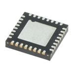
| 描述 | IC CLK BUFFER 2:10 3GHZ 32QFN时钟驱动器及分配 BBG ECL CLOCK DIST CHIP |
| 产品分类 | |
| 品牌 | ON Semiconductor |
| 产品手册 | |
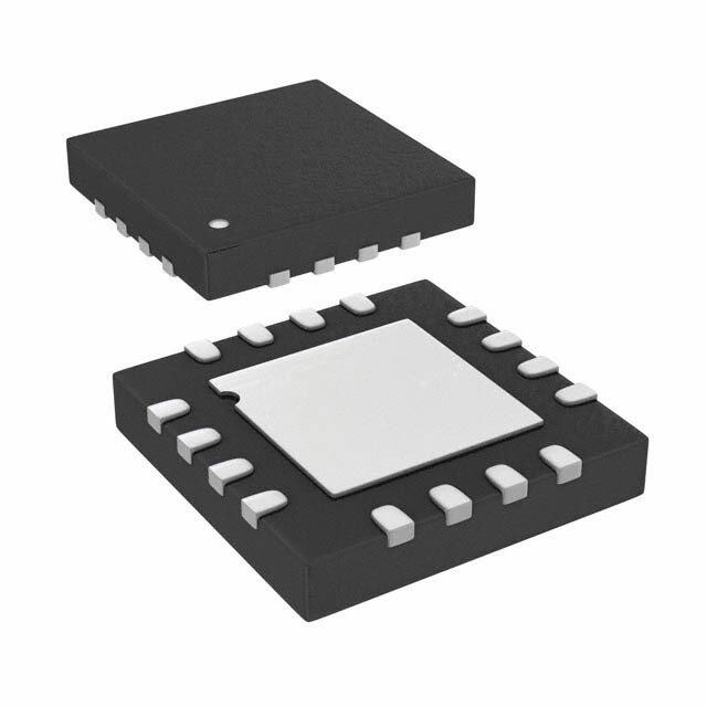
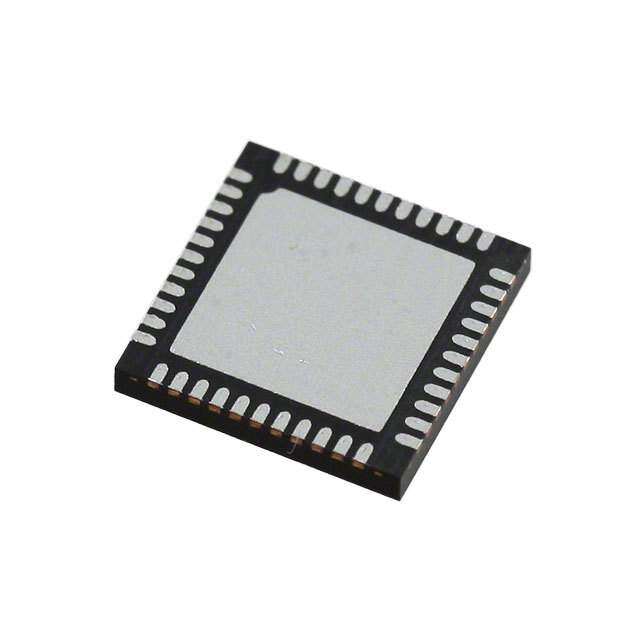
| 产品图片 |
|
| rohs | 符合RoHS无铅 / 符合限制有害物质指令(RoHS)规范要求 |
| 产品系列 | 时钟和计时器IC,时钟驱动器及分配,ON Semiconductor MC100LVEP111MNG100LVEP |
| 数据手册 | |
| 产品型号 | MC100LVEP111MNG |
| 乘法/除法因子 | 1:10 |
| 产品种类 | 时钟驱动器及分配 |
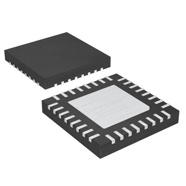
| 供应商器件封装 | 32-QFN(5x5) |
| 其它名称 | MC100LVEP111MNG-ND |
| 包装 | 管件 |
| 商标 | ON Semiconductor |
| 安装类型 | 表面贴装 |
| 安装风格 | SMD/SMT |
| 封装/外壳 | 32-VFQFN 裸露焊盘 |
| 封装/箱体 | QFN-32 |
| 工作温度 | -40°C ~ 85°C |
| 工厂包装数量 | 74 |
| 差分-输入:输出 | 是/是 |
| 最大工作温度 | + 85 C |
| 最大输出频率 | 3 GHz |
| 最小工作温度 | - 40 C |
| 标准包装 | 74 |
| 比率-输入:输出 | 2:10 |
| 电压-电源 | 2.375 V ~ 3.8 V |
| 电源电压-最大 | 3.8 V |
| 电源电压-最小 | 2.375 V |
| 电源电流 | 90 mA |
| 电路数 | 1 |
| 类型 | ECL, HSTL, PECL |
| 系列 | MC100LVEP111 |
| 输入 | ECL,HSTL,LVDS,PECL |
| 输入类型 | LVECL, LVPECL |
| 输出 | ECL,PECL |
| 输出类型 | ECL, PECL |
| 零件号别名 | MC100LVEP111FAG |
| 频率-最大值 | 3GHz |

%20Renders/32-VQFN%20Exposed%20Pad.jpg)


- 商务部:美国ITC正式对集成电路等产品启动337调查
- 曝三星4nm工艺存在良率问题 高通将骁龙8 Gen1或转产台积电
- 太阳诱电将投资9.5亿元在常州建新厂生产MLCC 预计2023年完工
- 英特尔发布欧洲新工厂建设计划 深化IDM 2.0 战略
- 台积电先进制程称霸业界 有大客户加持明年业绩稳了
- 达到5530亿美元!SIA预计今年全球半导体销售额将创下新高
- 英特尔拟将自动驾驶子公司Mobileye上市 估值或超500亿美元
- 三星加码芯片和SET,合并消费电子和移动部门,撤换高东真等 CEO
- 三星电子宣布重大人事变动 还合并消费电子和移动部门
- 海关总署:前11个月进口集成电路产品价值2.52万亿元 增长14.8%


PDF Datasheet 数据手册内容提取
MC100LVEP111 2.5V / 3.3V 2:1:10 Differential ECL/PECL/HSTL Clock Driver Description www.onsemi.com The MC100LVEP111 is a low skew 2:1:10 differential driver, designed with clock distribution in mind, accepting two clock sources into an input MARKING multiplexer. The PECL input signals can be either differential or DIAGRAMS* single−ended (if the V output is used). HSTL inputs can be used when BB the LVEP111 is operating under PECL conditions. The LVEP111 specifically guarantees low output−to−output skew. Optimal design, layout, and processing minimize skew within a device and MC100 from device to device. LVEP111 To ensure tightest skew, both sides of differential outputs identically AWLYYWWG terminate into 50 (cid:2) even if only one output is being used. If an output LQFP−32 32 pair is unused, both outputs may be left open (unterminated) without FA SUFFIX affecting skew. CASE 873A 1 The MC100LVEP111, as with most other ECL devices, can be operated from a positive V supply in PECL mode. This allows the CC LVEP111 to be used for high performance clock distribution in +3.3 V or 1 +2.5 V systems. Single−ended CLK input operation is limited to a V ≥ MC100 CC 1 32 3.0 V in PECL mode, or V (cid:2) −3.0 V in NECL mode when using VBB LVEP111 EE QFN32 AWLYYWW (See Figure 11). Full operating range is available when using an external MN SUFFIX (cid:2) voltage reference (See Figure 10). Designers can take advantage of the CASE 488AM LVEP111’s performance to distribute low skew clocks across the backplane or the board. A = Assembly Location WL = Wafer Lot Features YY = Year • 85 ps Typical Device−to−Device Skew WW = Work Week • G or (cid:2) = Pb−Free Package 20 ps Typical Output−to−Output Skew • Jitter Less than 1 ps RMS *For additional marking information, refer to • Application Note AND8002/D. Additive RMS Phase Jitter: 60 fs @ 156.25 MHz, Typ. • Maximum Frequency > 3 GHz Typical • ORDERING INFORMATION V Output BB See detailed ordering and shipping information in the package • 430 ps Typical Propagation Delay dimensions section on page 11 of this data sheet. • The 100 Series Contains Temperature Compensation • PECL and HSTL Mode Operating Range: V = 2.375 V to 3.8 V CC with V = 0 V EE • NECL Mode Operating Range: V = 0 V CC with V = −2.375 V to −3.8 V EE • Open Input Default State • LVDS Input Compatible • Fully Compatible with MC100EP111 • These are Pb−Free Devices © Semiconductor Components Industries, LLC, 2015 1 Publication Order Number: August, 2015 − Rev. 23 MC100LVEP111/D
MC100LVEP111 Q3 Q3 Q4 Q4 Q5 Q5 Q6 Q6 Table 1. PIN DESCRIPTION PIN FUNCTION 24 23 22 21 20 19 18 17 CLK0*, CLK0** ECL/PECL/HSTL CLK Input VCC 25 16 VCC CLK1*, CLK1** ECL/PECL/HSTL CLK Input Q2 26 15 Q7 Q0:9, Q0:9 ECL/PECL Outputs CLK_SEL* ECL/PECL Active Clock Select Input Q2 27 14 Q7 VBB Reference Voltage Output Q1 28 13 Q8 MC100LVEP111 VCC Positive Supply Q1 29 12 Q8 VEE Negative Supply Q0 30 11 Q9 EP The exposed pad (EP) on the package Q0 31 10 Q9 bottom must be attached to a heat−sink- ing conduit. The exposed pad may only VCC 32 9 VCC 1 2 3 4 5 6 7 8 be electrically connected to VEE. * Pins will default LOW when left open. ** Pins will default to 2/3VCC when left open. VCC EL K0 K0 VBB K1 K1 VEE S L L L L Table 2. FUNCTION TABLE _ C C C C K L C CLK_SEL Active Input Warning: All VCC and VEE pins must be externally connected L CLK0, CLK0 to Power Supply to guarantee proper operation. H CLK1, CLK1 Figure 1. LQFP−32 Pinout (Top View) VCC Q0 Q0 Q1 Q1 Q2 Q2 VCC 32 31 30 29 28 27 26 25 VCC 1 24 Q3 CLK_SEL 2 23 Q3 CLK0 3 22 Q4 CLK0 4 21 Q4 MC100LVEP111 VBB 5 20 Q5 CLK1 6 19 Q5 CLK1 7 18 Q6 VEE 8 17 Q6 9 10 11 12 13 14 15 16 VCC Q9 Q9 Q8 Q8 Q7 Q7 VCC Exposed Pad (EP) Figure 2. QFN−32 Pinout (Top View) www.onsemi.com 2
MC100LVEP111 Table 3. ATTRIBUTES Characteristics Value Internal Input Pulldown Resistor 75 k(cid:2) Internal Input Pullup Resistor 37.5 k(cid:2) ESD Protection Human Body Model > 2 kV Machine Model > 100 V Charged Device Model > 2 kV Moisture Sensitivity (Note 1) Pb Pkgs Pb−Free Pkgs LQFP Level 2 Level 2 QFN Level 1 Level 1 Flammability Rating Oxygen Index: 28 to 34 UL 94 V−0 @ 0.125 in Transistor Count 602 Devices Meets or exceeds JEDEC Spec EIA/JESD78 IC Latchup Test 1. For additional information, refer to Application Note AND8003/D. Q0 Q0 Q1 Q1 Q2 Q2 Q3 Q3 CLK0 Q4 0 CLK0 Q4 Q5 CLK1 Q5 1 CLK1 Q6 VBB Q6 CLK_SEL VEE Q7 Q7 Q8 VCC Q8 Q9 Q9 Figure 3. Logic Diagram www.onsemi.com 3
MC100LVEP111 Table 4. MAXIMUM RATINGS Symbol Parameter Condition 1 Condition 2 Rating Unit VCC PECL Mode Power Supply VEE = 0 V 6 V VEE NECL Mode Power Supply VCC = 0 V −6 V VI PECL Mode Input Voltage VEE = 0 V VI ≤ VCC 6 V NECL Mode Input Voltage VCC = 0 V VI ≥ VEE −6 V Iout Output Current Continuous 50 mA Surge 100 mA IBB VBB Sink/Source ± 0.5 mA TA Operating Temperature Range −40 to +85 °C Tstg Storage Temperature Range −65 to +150 °C (cid:3) Thermal Resistance (Junction−to−Ambient) 0 lfpm LQFP−32 80 °C/W JA 500 lfpm LQFP−32 55 °C/W (cid:3) Thermal Resistance (Junction−to−Case) Standard Board LQFP−32 12 to 17 °C/W JC (cid:3) Thermal Resistance (Junction−to−Ambient) 0 lfpm QFN−32 31 °C/W JA 500 lfpm QFN−32 27 °C/W (cid:3) Thermal Resistance (Junction−to−Case) 2S2P QFN−32 12 °C/W JC Tsol Wave Solder Pb < 3 sec @ 248°C 265 °C Pb−Free (QFN−32 Only) < 3 sec @ 260°C 265 Stresses exceeding those listed in the Maximum Ratings table may damage the device. If any of these limits are exceeded, device functionality should not be assumed, damage may occur and reliability may be affected. www.onsemi.com 4
MC100LVEP111 Table 5. PECL DC CHARACTERISTICS VCC = 2.5 V; VEE = 0 V (Note 2) −40°C 25°C 85°C Symbol Characteristic Min Typ Max Min Typ Max Min Typ Max Unit IEE Power Supply Current 60 90 120 60 90 120 60 90 120 mA VOH Output HIGH Voltage (Note 3) 1355 1480 1605 1355 1480 1605 1355 1480 1605 mV VOL Output LOW Voltage (Note 3) 505 730 900 505 730 900 505 730 900 mV VIH Input HIGH Voltage (Single−Ended) 1335 1620 1335 1620 1275 1620 mV (Note 4) VIL Input LOW Voltage (Single−Ended) 505 875 505 875 505 875 mV (Note 4) VIHCMR Input HIGH Voltage Common Mode 1.2 2.5 1.2 2.5 1.2 2.5 V Range (Differential Configuration) (Note 5) IIH Input HIGH Current 150 150 150 (cid:4)A IIL Input LOW Current CLK 0.5 0.5 0.5 (cid:4)A CLK −150 −150 −150 NOTE:Device will meet the specifications after thermal equilibrium has been established when mounted in a test socket or printed circuit board with maintained transverse airflow greater than 500 lfpm. 2. Input and output parameters vary 1:1 with VCC. VEE can vary + 0.125 V to −1.3 V. 3. All loading with 50 (cid:2) to VEE. 4. Do not use VBB at VCC < 3.0 V. 5. VIHCMR min varies 1:1 with VEE, VIHCMR max varies 1:1 with VCC. The VIHCMR range is referenced to the most positive side of the differential input signal. Table 6. PECL DC CHARACTERISTICS VCC = 3.3 V; VEE = 0 V (Note 6) −40°C 25°C 85°C Symbol Characteristic Min Typ Max Min Typ Max Min Typ Max Unit IEE Power Supply Current 60 90 120 60 90 120 60 90 120 mA VOH Output HIGH Voltage (Note 7) 2155 2280 2405 2155 2280 2405 2155 2280 2405 mV VOL Output LOW Voltage (Note 7) 1305 1530 1700 1305 1530 1700 1305 1530 1700 mV VIH Input HIGH Voltage (Single−Ended) 2135 2420 2135 2420 2135 2420 mV VIL Input LOW Voltage (Single−Ended) 1305 1675 1305 1675 1305 1675 mV VBB Output Reference Voltage (Note 8) 1775 1875 1975 1775 1875 1975 1775 1875 1975 mV VIHCMR Input HIGH Voltage Common Mode 1.2 3.3 1.2 3.3 1.2 3.3 V Range (Differential Configuration) (Note 9) IIH Input HIGH Current 150 150 150 (cid:4)A IIL Input LOW Current CLK 0.5 0.5 0.5 (cid:4)A CLK −150 −150 −150 NOTE:Device will meet the specifications after thermal equilibrium has been established when mounted in a test socket or printed circuit board with maintained transverse airflow greater than 500 lfpm. 6. Input and output parameters vary 1:1 with VCC. VEE can vary + 0.925 V to −0.5 V. 7. All loading with 50 (cid:2) to VCC − 2.0 V. 8. Single ended input operation is limited VCC ≥ 3.0 V in PECL mode. 9. VIHCMR min varies 1:1 with VEE, VIHCMR max varies 1:1 with VCC. The VIHCMR range is referenced to the most positive side of the differential input signal. Table 7. NECL DC CHARACTERISTICS VCC = 0 V, VEE = −2.375 V to −3.8 V (Note 10) −40°C 25°C 85°C Symbol Characteristic Min Typ Max Min Typ Max Min Typ Max Unit IEE Power Supply Current 60 90 120 60 90 120 60 90 120 mA VOH Output HIGH Voltage (Note 11) −1145 −1020 −895 −1145 −1020 −895 −1145 −1020 −895 mV VOL Output LOW Voltage (Note 11) −1995 −1770 −1600 −1995 −1770 −1600 −1995 −1770 −1600 mV www.onsemi.com 5
MC100LVEP111 Table 7. NECL DC CHARACTERISTICS VCC = 0 V, VEE = −2.375 V to −3.8 V (Note 10) −40°C 25°C 85°C Symbol Characteristic Min Typ Max Min Typ Max Min Typ Max Unit VIH Input HIGH Voltage (Single−Ended) −1165 −880 −1165 −880 −1165 −880 mV VIL Input LOW Voltage (Single−Ended) −1995 −1625 −1995 −1625 −1995 −1625 mV VBB Output Reference Voltage (Note 12) −1525 −1425 −1325 −1525 −1425 −1325 −1525 −1425 −1325 mV VIHCMR Input HIGH Voltage Common Mode VEE + 1.2 0.0 VEE + 1.2 0.0 VEE + 1.2 0.0 V Range (Differential Configuration) (Note 13) IIH Input HIGH Current 150 150 150 (cid:4)A IIL Input LOW Current CLK 0.5 0.5 0.5 (cid:4)A CLK −150 −150 −150 NOTE:Device will meet the specifications after thermal equilibrium has been established when mounted in a test socket or printed circuit board with maintained transverse airflow greater than 500 lfpm. 10.Input and output parameters vary 1:1 with VCC. 11.All loading with 50 (cid:2) to VCC − 2.0 V. 12.Single ended input operation is limited VEE ≤ −3.0V in NECL mode. 13.VIHCMR min varies 1:1 with VEE, VIHCMR max varies 1:1 with VCC. The VIHCMR range is referenced to the most positive side of the differential input signal. Table 8. HSTL DC CHARACTERISTICS VCC = 2.375 to 3.8 V, VEE = 0 V −40°C 25°C 85°C Symbol Characteristic Min Typ Max Min Typ Max Min Typ Max Unit VIH Input HIGH Voltage 1200 1200 1200 mV VIL Input LOW Voltage 400 400 400 mV Vx Input Crossover Voltage 680 900 680 900 680 900 mV ICC Power Supply Current 70 100 120 70 100 120 70 100 120 mA NOTE:Device will meet the specifications after thermal equilibrium has been established when mounted in a test socket or printed circuit board with maintained transverse airflow greater than 500 lfpm. www.onsemi.com 6
MC100LVEP111 Table 9. AC CHARACTERISTICS VCC = 0 V; VEE = −2.375 to −3.8 V or VCC = 2.375 to 3.8 V; VEE = 0 V (Note 14) −40°C 25°C 85°C Symbol Characteristic Min Typ Max Min Typ Max Min Typ Max Unit fmaxPECL/HSTL Maximum Frequency (Figure 4) 3 3 3 GHz tPLH Propagation Delay 325 400 475 350 430 500 375 510 590 ps tPHL (Differential Configuration) tskew Within−Device Skew (Note 15) 20 25 20 25 25 35 ps Within−Device Skew @ 2.5 V (Note 15) 20 25 20 25 20 25 Device−to−Device Skew (Note 16) 85 150 85 150 85 150 tJITTER CLOCK Random Jitter (RMS) ps @ (cid:2)0.5 GHz 0.209 0.5 0.204 0.5 0.221 0.5 @ (cid:2)1.0 GHz 0.200 0.5 0.214 0.6 0.229 0.5 @ (cid:2)1.5 GHz 0.197 0.4 0.213 0.5 0.243 0.4 @ (cid:2)2.0 GHz 0.220 0.5 0.224 0.5 0.292 0.6 @ (cid:2)2.5 GHz 0.232 0.4 0.290 0.5 0.522 0.8 @ (cid:2)3.0 GHz 0.348 0.6 0.545 0.8 0.911 1.3 tjit((cid:5)) Additive RMS Phase Jitter 60 fs fc = 156.25 MHz, Integration Range: 12 kHz to 20 MHz (See Figure 5) VPP Input Swing (Differential Interconnect 150 800 1200 150 800 1200 150 800 1200 mV Configuration) Measured Single−Ended tr/tf Output Rise/Fall Time (20%−80%) 105 200 255 125 200 275 150 230 320 ps NOTE:Device will meet the specifications after thermal equilibrium has been established when mounted in a test socket or printed circuit board with maintained transverse airflow greater than 500 lfpm. 14.Measured with 750 mV source, 50% duty cycle clock source. All loading with 50 (cid:2) to VCC − 2.0 V. 15.Skew is measured between outputs under identical transitions and conditions on any one device. 16.Device−to−Device skew for identical transitions at identical VCC levels. 800 700 V) 600 m ( pp 500 T U O V 400 300 200 100 0 0 1000 2000 3000 4000 5000 6000 FREQUENCY (MHz) Figure 4. Fmax Typical www.onsemi.com 7
MC100LVEP111 Figure 5. Typical MC100LVEP111 Phase Noise Plot at fCarrier = 156.25 MHz, VCC = 3.3 V, 25(cid:2)C The above phase noise data was captured using Agilent notably lower than that of the DUT. If the phase noise of the E5052A/B. The data displays the input phase noise and source is greater than the noise floor of the device under test, output phase noise used to calculate the additive phase jitter the source noise will dominate the additive phase jitter at a specified integration range. The additive RMS phase calculation and lead to an incorrect negative result for the jitter contributed by the device (integrated between 12 kHz additive phase noise within the integration range. The and 20 MHz) is 53 fs. The additive RMS phase jitter Figure above is a good example of the MC100LVEP111 performance of the fanout buffer is highly dependent on the source generator phase noise having a significantly lower phase noise of the input source. floor than the DUT and results in an additive phase jitter of To obtain the most precise additive phase noise 53 fs. measurement, it is vital that the source phase noise be Additive RMS phase jitter = √RMS phase jitter of output2 − RMS phase jitter of input2 (cid:5) 53fs(cid:3) 138.18fs2(cid:4)127.59fs2 Figure 5 was created with measured data from phase noise and jitter analysis of timing devices and clock Agilent−E5052B Signal Source Analyzer using ON tree designs. To see the performance of MC100LVEP111 Semiconductor Phase Noise Explorer web tool. This free beyond conditions outlined in this datasheet, please visit the application enables an interactive environment for advanced ON Semiconductor Green Point Design Tools homepage. www.onsemi.com 8
MC100LVEP111 VCC VCC VCC VCC Z0 = 50 (cid:2) MC100LVEP111 Z0 = 50 (cid:2) MC100LVEP111 CLKx CLKx 50 (cid:2)(cid:6) 50 (cid:2) LVPECL LVDS VTT 100 (cid:2) Driver Driver 50 (cid:2) Z0 = 50 (cid:2) 50 (cid:2)(cid:6) CLK CLK Z0 = 50 (cid:2) VT = VCC − 2.0 V VEE VEE GND GND Figure 6. LVPECL in Interface Figure 7. LVDS in Interface VCC VCC VCC VCC Z0 = 50 (cid:2) MC100LVEP111 Z0 = 50 (cid:2) MC100LVEP111 CLKx CLKx 50 (cid:2) 50 (cid:2) HSTL CML Driver VDDQ Driver VCC 50 (cid:2) 50 (cid:2) CLK CLK Z0 = 50 (cid:2) Z0 = 50 (cid:2) VEE VEE VEE VEE Figure 8. HSTL in Interface Figure 9. Standard 50 (cid:2) Load CML in Interface www.onsemi.com 9
MC100LVEP111 VCC VCC Z0 = 50 (cid:2) MC100LVEP111 CLKx LVCMOS LVTTL Sin- VCC gle−Ended Driver 1k CLK 1k VEE VEE Figure 10. Single−Ended Interface LVCMOS/LVTTL in Interface Using an External Voltage Reference VCC VCC Z0 = 50 (cid:2) MC100LVEP111 CLKx LVCMOS LVTTL Sin- gle−Ended Driver CLK VEE VEE VBB VEE Figure 11. Single−Ended Interface LVCMOS/LVTTL in Interface Using V BB www.onsemi.com 10
MC100LVEP111 Q Zo = 50 (cid:2) D Driver Receiver Device Device Q Zo = 50 (cid:2) D 50 (cid:2) 50 (cid:2) VTT VTT = VCC − 2.0 V Figure 12. Typical Termination for Output Driver and Device Evaluation (See Application Note AND8020/D − Termination of ECL Logic Devices.) Round Sprocket Holes Quadrant Quadrant A B Designations User Direction Quadrant A = Upper Left Quadrant B = Upper Right of Unreeling Quadrant C = Lower Left Quadrant Quadrant Quadrant D = Lower Right C D Figure 13. Tape and Reel Pin 1 Quadrant Orientation ORDERING INFORMATION Device Package Shipping† MC100LVEP111FAG LQFP−32 250 Units / Tray (Pb−Free) MC100LVEP111FARG LQFP−32 2000 / Tape & Reel (Pb−Free) (Pin 1 Orientation in Quadrant B, Figure 13) M100LVEP111FATWG LQFP−32 2000 / Tape & Reel (Pb−Free) (Pin 1 Orientation in Quadrant A, Figure 13) MC100LVEP111MNG QFN−32 74 Units / Rail (Pb−Free) MC100LVEP111MNRG QFN−32 1000 / Tape & Reel (Pb−Free) †For information on tape and reel specifications, including part orientation and tape sizes, please refer to our Tape and Reel Packaging Specifications Brochure, BRD8011/D. www.onsemi.com 11
MC100LVEP111 Resource Reference of Application Notes AN1405/D − ECL Clock Distribution Techniques AN1406/D − Designing with PECL (ECL at +5.0 V) AN1503/D − ECLinPS(cid:3) I/O SPiCE Modeling Kit AN1504/D − Metastability and the ECLinPS Family AN1568/D − Interfacing Between LVDS and ECL AN1672/D − The ECL Translator Guide AND8001/D − Odd Number Counters Design AND8002/D − Marking and Date Codes AND8020/D − Termination of ECL Logic Devices AND8066/D − Interfacing with ECLinPS AND8090/D − AC Characteristics of ECL Devices www.onsemi.com 12
MC100LVEP111 PACKAGE DIMENSIONS 32 LEAD LQFP CASE 873A−02 ISSUE C − Z A1 A 4X 0.20 (0.008) AB T-U Z U−, − 32 25 − −, T − 1 −T− −U− AE B V P B1 DETAIL Y V1 BASE Z 8 17 AE METAL U - T DETAIL Y N 9 ÉÉ AC 9 S1 −Z− 4X 0.20 (0.008) AC T-U Z ÉF É D 8)M 0 S ÉÉ 0.0 0 ( 8XM(cid:4) J 0.2 R DETAIL AD G SECTION AE−AE −AB− E C SEATING −AC− PLANE 0.10 (0.004) AC H W K Q(cid:4) 0) DETAIL AD X GE PLANE 50 (0.01 NOTES: MILLIMETERS INCHES GAU 0.2 1. DIMENSIONING AND TOLERANCING PER ANSI Y14.5M, 1982. DIM MIN MAX MIN MAX 2. CONTROLLING DIMENSION: A 7.000 BSC 0.276 BSC MILLIMETER. A1 3.500 BSC 0.138 BSC 3. DATUM PLANE −AB− IS LOCATED AT B 7.000 BSC 0.276 BSC BOTTOM OF LEAD AND IS COINCIDENT B1 3.500 BSC 0.138 BSC WITH THE LEAD WHERE THE LEAD C 1.400 1.600 0.055 0.063 EXITS THE PLASTIC BODY AT THE D 0.300 0.450 0.012 0.018 BOTTOM OF THE PARTING LINE. E 1.350 1.450 0.053 0.057 4. DATUMS −T−, −U−, AND −Z− TO BE F 0.300 0.400 0.012 0.016 DETERMINED AT DATUM PLANE −AB−. G 0.800 BSC 0.031 BSC 5. DIMENSIONS S AND V TO BE H 0.050 0.150 0.002 0.006 DETERMINED AT SEATING PLANE −AC−. J 0.090 0.200 0.004 0.008 6. DIMENSIONS A AND B DO NOT INCLUDE K 0.450 0.750 0.018 0.030 MPROOLTDR PURSOIOTNR UISS I0O.2N5. 0 A(0L.L0O10W) APBELRE SIDE. M 12(cid:4) REF 12(cid:4) REF DIMENSIONS A AND B DO INCLUDE N 0.090 0.160 0.004 0.006 MOLD MISMATCH AND ARE P 0.400 BSC 0.016 BSC DETERMINED AT DATUM PLANE −AB−. Q 1(cid:4) 5 (cid:4) 1(cid:4) 5 (cid:4) 7. DIMENSION D DOES NOT INCLUDE R 0.150 0.250 0.006 0.010 DAMBAR PROTRUSION. DAMBAR S 9.000 BSC 0.354 BSC PROTRUSION SHALL NOT CAUSE THE S1 4.500 BSC 0.177 BSC D DIMENSION TO EXCEED 0.520 (0.020). V 9.000 BSC 0.354 BSC 8. MINIMUM SOLDER PLATE THICKNESS V1 4.500 BSC 0.177 BSC SHALL BE 0.0076 (0.0003). W 0.200 REF 0.008 REF 9. EXACT SHAPE OF EACH CORNER MAY X 1.000 REF 0.039 REF VARY FROM DEPICTION. www.onsemi.com 13
MC100LVEP111 PACKAGE DIMENSIONS QFN32 5x5, 0.5 P CASE 488AM ISSUE A D A L L NOTES: B 1. DIMENSIONS AND TOLERANCING PER ASME Y14.5M, 1994. ÉÉ 2. CONTROLLING DIMENSION: MILLIMETERS. LPOICNA OTNIOEN L1 3. DIMENSION b APPLIES TO PLATED ÉÉ TERMINAL AND IS MEASURED BETWEEN DETAIL A 0.15 AND 0.30MM FROM THE TERMINAL TIP. 4. COPLANARITY APPLIES TO THE EXPOSED ALTERNATE TERMINAL E CONSTRUCTIONS PAD AS WELL AS THE TERMINALS. MILLIMETERS DIM MIN MAX 0.15 C A 0.80 1.00 A1 −−− 0.05 A3 0.20 REF 0.15 C TOP VIEW EXPOSED Cu MOLD CMPD b 0.18 0.30 ÉÇÉÇÉÇ D 5.00 BSC D2 2.95 3.25 0.10 C DETAIL B A (A3) ÇÇÇ EE2 2.59.500 BS3C.25 A1 DETAIL B e 0.50 BSC ALTERNATE K 0.20 −−− 0.08 C CONSTRUCTION L 0.30 0.50 L1 −−− 0.15 NOTE 4 SIDE VIEW C SPELAATNIENG RECOMMENDED DETAIL A SOLDERING FOOTPRINT* D2 K 9 5.30 32X 8 17 3.35 0.63 32X L E2 1 3.35 5.30 32 25 32Xb e 0.10 M C A B e/2 0.05 M C NOTE 3 BOTTOM VIEW 0.50 32X PITCH 0.30 DIMENSION: MILLIMETERS *For additional information on our Pb−Free strategy and soldering details, please download the ON Semiconductor Soldering and Mounting Techniques Reference Manual, SOLDERRM/D. ECLinPS is a trademark of Semiconductor Components Industries, LLC (SCILLC). ON Semiconductor and are registered trademarks of Semiconductor Components Industries, LLC (SCILLC). SCILLC owns the rights to a number of patents, trademarks, copyrights, trade secrets, and other intellectual property. A listing of SCILLC’s product/patent coverage may be accessed at www.onsemi.com/site/pdf/Patent−Marking.pdf. SCILLC reserves the right to make changes without further notice to any products herein. SCILLC makes no warranty, representation or guarantee regarding the suitability of its products for any particular purpose, nor does SCILLC assume any liability arising out of the application or use of any product or circuit, and specifically disclaims any and all liability, including without limitation special, consequential or incidental damages. “Typical” parameters which may be provided in SCILLC data sheets and/or specifications can and do vary in different applications and actual performance may vary over time. All operating parameters, including “Typicals” must be validated for each customer application by customer’s technical experts. SCILLC does not convey any license under its patent rights nor the rights of others. SCILLC products are not designed, intended, or authorized for use as components in systems intended for surgical implant into the body, or other applications intended to support or sustain life, or for any other application in which the failure of the SCILLC product could create a situation where personal injury or death may occur. Should Buyer purchase or use SCILLC products for any such unintended or unauthorized application, Buyer shall indemnify and hold SCILLC and its officers, employees, subsidiaries, affiliates, and distributors harmless against all claims, costs, damages, and expenses, and reasonable attorney fees arising out of, directly or indirectly, any claim of personal injury or death associated with such unintended or unauthorized use, even if such claim alleges that SCILLC was negligent regarding the design or manufacture of the part. SCILLC is an Equal Opportunity/Affirmative Action Employer. This literature is subject to all applicable copyright laws and is not for resale in any manner. PUBLICATION ORDERING INFORMATION LITERATURE FULFILLMENT: N. American Technical Support: 800−282−9855 Toll Free ON Semiconductor Website: www.onsemi.com Literature Distribution Center for ON Semiconductor USA/Canada P.O. Box 5163, Denver, Colorado 80217 USA Europe, Middle East and Africa Technical Support: Order Literature: http://www.onsemi.com/orderlit Phone: 303−675−2175 or 800−344−3860 Toll Free USA/Canada Phone: 421 33 790 2910 Fax: 303−675−2176 or 800−344−3867 Toll Free USA/Canada Japan Customer Focus Center For additional information, please contact your local Email: orderlit@onsemi.com Phone: 81−3−5817−1050 Sales Representative www.onsemi.com MC100LVEP111/D 14
Mouser Electronics Authorized Distributor Click to View Pricing, Inventory, Delivery & Lifecycle Information: O N Semiconductor: MC100LVEP111MNG MC100LVEP111MNRG MC100LVEP111FAG MC100LVEP111FARG M100LVEP111FATWG