ICGOO在线商城 > 分立半导体产品 > 二极管 - 整流器 - 阵列 > MBRB2545CTG
 Datasheet下载
- 型号: MBRB2545CTG
- 制造商: ON Semiconductor
- 库位|库存: xxxx|xxxx
- 要求:
| 数量阶梯 | 香港交货 | 国内含税 |
| +xxxx | $xxxx | ¥xxxx |
查看当月历史价格
查看今年历史价格
MBRB2545CTG产品简介:
ICGOO电子元器件商城为您提供MBRB2545CTG由ON Semiconductor设计生产,在icgoo商城现货销售,并且可以通过原厂、代理商等渠道进行代购。 MBRB2545CTG价格参考¥3.70-¥5.46。ON SemiconductorMBRB2545CTG封装/规格:二极管 - 整流器 - 阵列, Diode Array 1 Pair Common Cathode Schottky 45V 15A Surface Mount TO-263-3, D²Pak (2 Leads + Tab), TO-263AB。您可以下载MBRB2545CTG参考资料、Datasheet数据手册功能说明书,资料中有MBRB2545CTG 详细功能的应用电路图电压和使用方法及教程。
ON Semiconductor(现为安森美半导体)的MBRB2545CTG是一款二极管整流器阵列,属于超快速恢复整流器系列。该型号具有低正向电压降(Vf)和低反向漏电流特性,适用于多种高效能电源管理应用场景。以下是其主要应用场景:

1. 开关电源(SMPS)
   MBRB2545CTG广泛应用于开关模式电源中,作为输出整流器或同步整流电路的一部分,提供高效的直流电转换。其超快恢复时间和低正向压降能够减少功率损耗,提高电源转换效率。

2. 逆变器与电机驱动
   在逆变器和电机驱动应用中,这款二极管可用于续流路径,保护电路免受反电动势的影响。其低反向恢复电荷(Qrr)特性有助于降低开关噪声和电磁干扰(EMI),从而提升系统稳定性。

3. 电池充电器
   该器件适合用于电池充电器中的整流电路,确保高效的能量传递并减少热量产生。其紧凑的设计也便于集成到小型化充电设备中。

4. 汽车电子
   在汽车电子领域,MBRB2545CTG可用于车载充电器、DC-DC转换器以及LED驱动电路等场景。其高可靠性和耐高温性能满足汽车环境的严苛要求。

5. 消费类电子产品
   这款二极管可应用于各种消费类电子产品,如笔记本电脑适配器、智能手机充电器和平板电脑电源模块,提供高效且稳定的电力供应。

6. 工业自动化
   在工业控制和自动化系统中,MBRB2545CTG可用于电源模块、信号调理电路以及传感器接口等场合,支持高效率和高可靠性的运行需求。

总之,MBRB2545CTG凭借其卓越的电气特性和可靠性,成为需要高效整流功能的各种应用的理想选择。
| 参数 | 数值 |
| 产品目录 | |
| 描述 | DIODE SCHOTTKY 45V 15A D2PAK肖特基二极管与整流器 30A 45V |
| 产品分类 | 二极管,整流器 - 阵列分离式半导体 |
| 品牌 | ON Semiconductor |
| 产品手册 | |
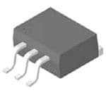
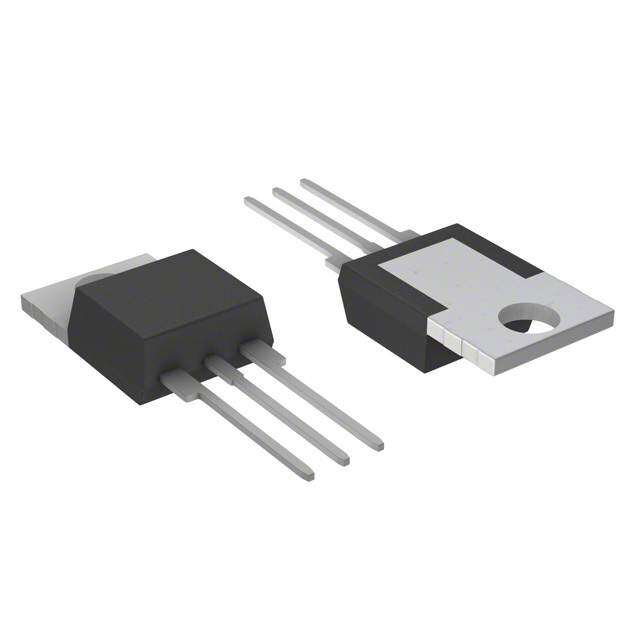
| 产品图片 |
|
| rohs | 符合RoHS无铅 / 符合限制有害物质指令(RoHS)规范要求 |
| 产品系列 | 二极管与整流器,肖特基二极管与整流器,ON Semiconductor MBRB2545CTGSWITCHMODE™ |
| 数据手册 | |
| 产品型号 | MBRB2545CTG |
| 不同If时的电压-正向(Vf) | 820mV @ 30A |
| 不同 Vr时的电流-反向漏电流 | 200µA @ 45V |
| 二极管类型 | |
| 二极管配置 | 1 对共阴极 |
| 产品 | Schottky Diodes |
| 产品目录页面 | |
| 产品种类 | 肖特基二极管与整流器 |
| 供应商器件封装 | D2PAK |
| 其它名称 | MBRB2545CTG-ND |
| 包装 | 管件 |
| 反向恢复时间(trr) | - |
| 商标 | ON Semiconductor |
| 安装类型 | 表面贴装 |
| 安装风格 | SMD/SMT |
| 封装 | Tube |
| 封装/外壳 | TO-263-3,D²Pak(2 引线+接片),TO-263AB |
| 封装/箱体 | D2PAK |
| 峰值反向电压 | 45 V |
| 工作温度范围 | - 65 C to + 175 C |
| 工厂包装数量 | 50 |
| 技术 | Silicon |
| 最大反向漏泄电流 | 200 uA |
| 最大工作温度 | + 175 C |
| 最大浪涌电流 | 150 A |
| 最小工作温度 | - 65 C |
| 标准包装 | 50 |
| 正向电压下降 | 0.82 V |
| 正向连续电流 | 30 A |
| 热阻 | 1.5°C/W Jc |
| 电压-DC反向(Vr)(最大值) | 45V |
| 电流-平均整流(Io)(每二极管) | 15A |
| 系列 | MBRB2545CT |
| 速度 | 快速恢复 =< 500 ns,> 200mA(Io) |
| 配置 | Dual Common Cathode |
| 零件号别名 | MBRB2545CTT4G |


- 商务部:美国ITC正式对集成电路等产品启动337调查
- 曝三星4nm工艺存在良率问题 高通将骁龙8 Gen1或转产台积电
- 太阳诱电将投资9.5亿元在常州建新厂生产MLCC 预计2023年完工
- 英特尔发布欧洲新工厂建设计划 深化IDM 2.0 战略
- 台积电先进制程称霸业界 有大客户加持明年业绩稳了
- 达到5530亿美元!SIA预计今年全球半导体销售额将创下新高
- 英特尔拟将自动驾驶子公司Mobileye上市 估值或超500亿美元
- 三星加码芯片和SET,合并消费电子和移动部门,撤换高东真等 CEO
- 三星电子宣布重大人事变动 还合并消费电子和移动部门
- 海关总署:前11个月进口集成电路产品价值2.52万亿元 增长14.8%


PDF Datasheet 数据手册内容提取
MBRB2545CTG, SBRB2545CTG SWITCHMODE Power Rectifier D2PAK Surface Mount Power Package http://onsemi.com The D2PAK Power Rectifier is a state−of−the−art device that employs the Schottky Barrier principle with a platinum barrier metal. SCHOTTKY BARRIER Features RECTIFIER • Center−Tap Configuration 30 AMPERES, 45 VOLTS • Guardring for Stress Protection • Low Forward Voltage • 175°C Operating Junction Temperature • Epoxy Meets UL 94 V−0 @ 0.125 in • Short Heat Sink Tab Manufactured − Not Sheared • Similar in Size to the Industry Standard TO−220 Package D2PAK • CASE 418B AEC−Q101 Qualified and PPAP Capable STYLE 3 • SBRB Prefix for Automotive and Other Applications Requiring Unique Site and Control Change Requirements 1 • All Packages are Pb−Free* 4 3 Mechanical Characteristics • Case: Epoxy, Molded, Epoxy Meets UL 94 V−0 MARKING DIAGRAM • Weight: 1.7 Grams (Approximately) • Finish: All External Surfaces Corrosion Resistant and Terminal Leads are Readily Solderable AY WW • Lead and Mounting Surface Temperature for Soldering Purposes: B2545G 260°C Max. for 10 Seconds AKA • Device Meets MSL1 Requirements • ESD Ratings: ♦ Machine Model = C (> 400 V) A = Assembly Location ♦ Human Body Model = 3B (> 8000 V) Y = Year WW = Work Week B2545 = Device Code G = Pb−Free Package AKA = Diode Polarity ORDERING INFORMATION See detailed ordering and shipping information in the package dimensions section on page 2 of this data sheet. *For additional information on our Pb−Free strategy and soldering details, please download the ON Semiconductor Soldering and Mounting Techniques Reference Manual, SOLDERRM/D. © Semiconductor Components Industries, LLC, 2013 1 Publication Order Number: November, 2013 − Rev. 12 MBRB2545CT/D
MBRB2545CTG, SBRB2545CTG MAXIMUM RATINGS (Per Leg) Rating Symbol Value Unit Peak Repetitive Reverse Voltage VRRM 45 V Working Peak Reverse Voltage VRWM DC Blocking Voltage VR Average Rectified Forward Current IF(AV) 15 A (Rated VR, TC = 164°C) Total Device 30 Peak Repetitive Forward Current IFRM A (Rated VR, Square Wave, 20 kHz, TC = 160°C) 30 Non−Repetitive Peak Surge Current IFSM A (Surge Applied at Rated Load Conditions Halfwave, Single Phase, 60 Hz) 150 Peak Repetitive Reverse Surge Current (2.0 (cid:2)s, 1.0 kHz) IRRM 1.0 A Storage Temperature Range Tstg −65 to +175 °C Operating Junction Temperature (Note 1) TJ −65 to +175 °C Voltage Rate of Change (Rated VR) dv/dt 10,000 V/(cid:2)s Stresses exceeding Maximum Ratings may damage the device. Maximum Ratings are stress ratings only. Functional operation above the Recommended Operating Conditions is not implied. Extended exposure to stresses above the Recommended Operating Conditions may affect device reliability. 1. The heat generated must be less than the thermal conductivity from Junction−to−Ambient: dPD/dTJ < 1/R(cid:3)JA. THERMAL CHARACTERISTICS (Per Leg) Characteristic Symbol Value Unit Thermal Resistance, °C/W Junction−to−Case R(cid:3)JC 1.5 Junction−to−Ambient (Note 2) R(cid:3)JA 50 2. When mounted using minimum recommended pad size on FR−4 board. ELECTRICAL CHARACTERISTICS (Per Diode) Symbol Characteristic Condition Min Typ Max Unit VF Instantaneous Forward Voltage IF = 15 Amp, TJ = 25°C − − 0.62 V (Note 3) IF = 15 Amp, TJ = 125°C − 0.50 0.57 IF = 30 Amp, TJ = 25°C − − 0.82 IF = 30 Amp, TJ = 125°C − 0.65 0.72 IR Instantaneous Reverse Current VR = 45 Volts, TJ = 25°C − − 0.2 mA (Note 3) VR = 45 Volts, TJ = 125°C − 9.0 25 3. Pulse Test: Pulse Width = 300 (cid:2)s, Duty Cycle ≤ 2.0%. ORDERING INFORMATION Device Package Shipping† MBRB2545CTG D2PAK 50 Units / Rail (Pb−Free) SBRB2545CTG D2PAK 50 Units / Rail (Pb−Free) MBRB2545CTT4G D2PAK 800 Units / Tape & Reel (Pb−Free) SBRB2545CTT4G D2PAK 800 Units / Tape & Reel (Pb−Free) †For information on tape and reel specifications, including part orientation and tape sizes, please refer to our Tape and Reel Packaging Specifications Brochure, BRD8011/D. http://onsemi.com 2
MBRB2545CTG, SBRB2545CTG S)1000 200 P M 100 A RENT ( 100 mA) 124000 TJ = 150°C CUR NT ( 4.0 125°C ORWARD 10 TJ = 125°C E CURRE 012...400 100°C OUS F 150°C EVERS 00..21 75°C NTANE 1.0 25°C I, RR 000...000421 25°C A T S 0.004 , INF 0.10 0.2 0.4 0.6 0.8 1.0 1.2 1.4 1.6 1.8 0.0020 10 20 30 40 50 I VF(cid:2), INSTANTANEOUS FORWARD VOLTAGE (VOLTS) VR, REVERSE VOLTAGE (VOLTS) Figure 1. Typical Forward Voltage, Per Leg Figure 2. Typical Reverse Current, Per Leg S) T T WA 32 A) 26 N ( SQUARE WAVE T ( 24 DC TIO 28 TJ = 125°C EN 22 DISSIPA 24 (RESISTIVE LOAD) IIPAVK = (cid:4) DC CURR 2108 SQUARE OWER 20 (CAPACITIVE 5 WARD 1164 P 16 LOADS) D 10 R 12 R O E FORWA 182 IIPAVK= 20 RAGE F 1086 RAG 4 AVE 4 , AVEV) 00 4 8 12 16 20 24 28 32 36 40 , F(AV) 20145 150 155 160 165 170 175 A I PF( IF, AVERAGE FORWARD CURRENT (AMPS) TC, CASE TEMPERATURE (°C) Figure 3. Typical Forward Power Dissipation Figure 4. Current Derating, Case per Leg http://onsemi.com 3
MBRB2545CTG, SBRB2545CTG PACKAGE DIMENSIONS D2PAK 3 CASE 418B−04 ISSUE K NOTES: C 1. DIMENSIONING AND TOLERANCING PER ANSI Y14.5M, 1982. E 2. CONTROLLING DIMENSION: INCH. V 3. 418B−01 THRU 418B−03 OBSOLETE, −B− NEW STANDARD 418B−04. W 4 INCHES MILLIMETERS DIM MIN MAX MIN MAX A 0.340 0.380 8.64 9.65 B 0.380 0.405 9.65 10.29 A C 0.160 0.190 4.06 4.83 S D 0.020 0.035 0.51 0.89 1 2 3 E 0.045 0.055 1.14 1.40 F 0.310 0.350 7.87 8.89 G 0.100 BSC 2.54 BSC −T− H 0.080 0.110 2.03 2.79 K J 0.018 0.025 0.46 0.64 SEATING W PLANE G J KL 00..009502 00..011702 21..2392 21..7893 M 0.280 0.320 7.11 8.13 H N 0.197 REF 5.00 REF D3 PL P 0.079 REF 2.00 REF 0.13 (0.005) M T B M R 0.039 REF 0.99 REF S 0.575 0.625 14.60 15.88 V 0.045 0.055 1.14 1.40 VARIABLE STYLE 3: CONFIGURATION PIN 1.ANODE ZONE N P 2.CATHODE R 3.ANODE U 4.CATHODE L L L M M M F F F VIEW W−W VIEW W−W VIEW W−W 1 2 3 SOLDERING FOOTPRINT* 10.49 8.38 16.155 2X 3.504 2X 1.016 5.080 PITCH DIMENSIONS: MILLIMETERS *For additional information on our Pb−Free strategy and soldering details, please download the ON Semiconductor Soldering and Mounting Techniques Reference Manual, SOLDERRM/D. http://onsemi.com 4
MBRB2545CTG, SBRB2545CTG ON Semiconductor and are registered trademarks of Semiconductor Components Industries, LLC (SCILLC). SCILLC reserves the right to make changes without further notice to any products herein. SCILLC makes no warranty, representation or guarantee regarding the suitability of its products for any particular purpose, nor does SCILLC assume any liability arising out of the application or use of any product or circuit, and specifically disclaims any and all liability, including without limitation special, consequential or incidental damages. “Typical” parameters which may be provided in SCILLC data sheets and/or specifications can and do vary in different applications and actual performance may vary over time. All operating parameters, including “Typicals” must be validated for each customer application by customer’s technical experts. SCILLC does not convey any license under its patent rights nor the rights of others. SCILLC products are not designed, intended, or authorized for use as components in systems intended for surgical implant into the body, or other applications intended to support or sustain life, or for any other application in which the failure of the SCILLC product could create a situation where personal injury or death may occur. Should Buyer purchase or use SCILLC products for any such unintended or unauthorized application, Buyer shall indemnify and hold SCILLC and its officers, employees, subsidiaries, affiliates, and distributors harmless against all claims, costs, damages, and expenses, and reasonable attorney fees arising out of, directly or indirectly, any claim of personal injury or death associated with such unintended or unauthorized use, even if such claim alleges that SCILLC was negligent regarding the design or manufacture of the part. SCILLC is an Equal Opportunity/Affirmative Action Employer. This literature is subject to all applicable copyright laws and is not for resale in any manner. PUBLICATION ORDERING INFORMATION LITERATURE FULFILLMENT: N. American Technical Support: 800−282−9855 Toll Free ON Semiconductor Website: www.onsemi.com Literature Distribution Center for ON Semiconductor USA/Canada P.O. Box 5163, Denver, Colorado 80217 USA Europe, Middle East and Africa Technical Support: Order Literature: http://www.onsemi.com/orderlit Phone: 303−675−2175 or 800−344−3860 Toll Free USA/Canada Phone: 421 33 790 2910 Fax: 303−675−2176 or 800−344−3867 Toll Free USA/Canada Japan Customer Focus Center For additional information, please contact your local Email: orderlit@onsemi.com Phone: 81−3−5817−1050 Sales Representative http://onsemi.com MBRB2545CT/D 5
Mouser Electronics Authorized Distributor Click to View Pricing, Inventory, Delivery & Lifecycle Information: O N Semiconductor: MBRB2545CTG MBRB2545CTT4G SBRB2545CTG