
 Datasheet下载
- 型号: MB85RS256APNF-G-JNE1
- 制造商: Fujitsu
- 库位|库存: xxxx|xxxx
- 要求:
| 数量阶梯 | 香港交货 | 国内含税 |
| +xxxx | $xxxx | ¥xxxx |
查看当月历史价格
查看今年历史价格
MB85RS256APNF-G-JNE1产品简介:
ICGOO电子元器件商城为您提供MB85RS256APNF-G-JNE1由Fujitsu设计生产,在icgoo商城现货销售,并且可以通过原厂、代理商等渠道进行代购。 MB85RS256APNF-G-JNE1价格参考¥71.49-¥71.49。FujitsuMB85RS256APNF-G-JNE1封装/规格:存储器, FRAM(铁电体 RAM) 存储器 IC 256Kb (32K x 8) SPI 25MHz 8-SOP。您可以下载MB85RS256APNF-G-JNE1参考资料、Datasheet数据手册功能说明书,资料中有MB85RS256APNF-G-JNE1 详细功能的应用电路图电压和使用方法及教程。
Fujitsu Electronics America, Inc. 生产的 MB85RS256APNF-G-JNE1 是一款存储器产品,具体来说是一款基于 FRAM(铁电随机存取存储器)技术的非易失性存储器。FRAM 技术结合了 SRAM 的高速读写性能和 EEPROM 的非易失性特点,使其在多种应用场景中表现出色。

 应用场景:

1. 工业自动化:
   - 在工业控制系统中,MB85RS256APNF-G-JNE1 可用于存储关键参数、配置数据和日志信息。由于其非易失性和高耐久性,即使在断电情况下也能保证数据的安全性和完整性,特别适合需要频繁写入的应用场景。

2. 医疗设备:
   - 医疗设备如监护仪、血糖仪等需要实时记录患者数据,并且要求数据存储具有高可靠性和低延迟。FRAM 的特性使得它能够在这些设备中提供快速的数据记录和存储,确保数据不会丢失。

3. 智能仪表:
   - 智能电表、水表和气表等计量设备需要长时间运行并记录大量的使用数据。MB85RS256APNF-G-JNE1 的低功耗和高写入次数特性非常适合这类应用,能够有效延长设备的使用寿命。

4. 物联网 (IoT) 设备:
   - 物联网设备通常需要在低功耗环境下工作,并且需要频繁地存储传感器数据。FRAM 的低功耗特性和快速读写速度使其成为物联网设备的理想选择,特别是在电池供电的环境中。

5. 汽车电子:
   - 汽车电子系统中,如车载诊断系统(OBD)、行车记录仪等,需要可靠的存储解决方案来记录车辆状态和行驶数据。MB85RS256APNF-G-JNE1 的高耐久性和抗辐射能力使其适用于汽车环境中的严苛条件。

6. 便携式电子产品:
   - 便携式电子产品如可穿戴设备、手持终端等需要小巧、低功耗且可靠的存储方案。FRAM 的小尺寸和低功耗特性使其成为这些设备的理想选择,能够在有限的空间内提供高效的存储功能。

总之,MB85RS256APNF-G-JNE1 的独特优势使其在各种对数据可靠性、低功耗和快速响应有较高要求的应用场景中表现出色,广泛应用于工业、医疗、智能仪表、物联网和汽车电子等领域。
| 参数 | 数值 |
| 产品目录 | 集成电路 (IC) |
| 描述 | IC FRAM 256KBIT 25MHZ 8SOP |
| 产品分类 | |
| 品牌 | Fujitsu Semiconductor America Inc |
| 数据手册 | |
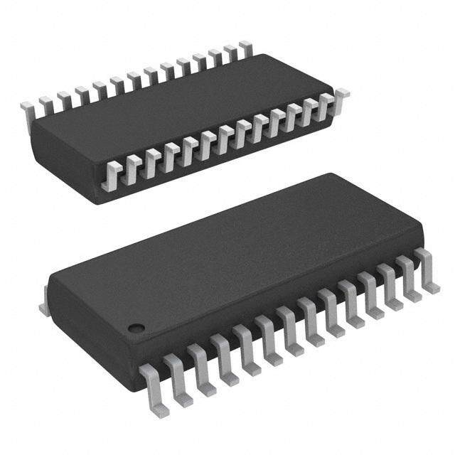
| 产品图片 |
|
| 产品型号 | MB85RS256APNF-G-JNE1 |
| rohs | 无铅 / 符合限制有害物质指令(RoHS)规范要求 |
| 产品系列 | - |
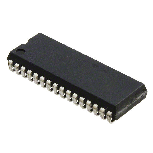
| 供应商器件封装 | 8-SOP |
| 其它名称 | 865-1177 |
| 包装 | 管件 |
| 存储器类型 | FRAM(Ferroelectric RAM) |
| 存储容量 | 256K (32K x 8) |
| 封装/外壳 | 8-SOIC(0.154",3.90mm 宽) |
| 工作温度 | -40°C ~ 85°C |
| 接口 | SPI 串行 |
| 标准包装 | 1,500 |
| 格式-存储器 | RAM |
| 特色产品 | http://www.digikey.com/product-highlights/cn/zh/fujitsu-fram/1208 |
| 电压-电源 | 3 V ~ 3.6 V |
| 速度 | 25MHz |


_renders/IS42S32800D-6BLI.jpg)


- 商务部:美国ITC正式对集成电路等产品启动337调查
- 曝三星4nm工艺存在良率问题 高通将骁龙8 Gen1或转产台积电
- 太阳诱电将投资9.5亿元在常州建新厂生产MLCC 预计2023年完工
- 英特尔发布欧洲新工厂建设计划 深化IDM 2.0 战略
- 台积电先进制程称霸业界 有大客户加持明年业绩稳了
- 达到5530亿美元!SIA预计今年全球半导体销售额将创下新高
- 英特尔拟将自动驾驶子公司Mobileye上市 估值或超500亿美元
- 三星加码芯片和SET,合并消费电子和移动部门,撤换高东真等 CEO
- 三星电子宣布重大人事变动 还合并消费电子和移动部门
- 海关总署:前11个月进口集成电路产品价值2.52万亿元 增长14.8%


PDF Datasheet 数据手册内容提取
FUJITSU SEMICONDUCTOR DATA SHEET DS501-00007-1v0-E Memory FRAM × 256 K (32 K 8) Bit SPI MB85RS256A ■ DESCRIPTION MB85RS256A is a FRAM (Ferroelectric Random Access Memory) chip in a configuration of 32,768 words × 8 bits, using the ferroelectric process and silicon gate CMOS process technologies for forming the nonvolatile memory cells. MB85RS256A adopts the Serial Peripheral Interface (SPI). The MB85RS256A is able to retain data without using a back-up battery, as is needed for SRAM. The memory cells used in the MB85RS256A can be used for 1010 read/write operations, which is a significant improvement over the number of read and write operations supported by Flash memory and E2PROM. MB85RS256A does not take long time to write data unlike Flash memories nor E2PROM, and MB85RS256A takes no wait time. ■ FEATURES • Bit configuration : 32,768 words × 8 bits (cid:129) Serial Peripheral Interface : SPI (Serial Peripheral Interface) Correspondent to SPI mode 0 (0, 0) and mode 3 (1, 1) (cid:129) Operating frequency : 25 MHz (Max) (cid:129) High endurance : 10 Billion Read/Writes (cid:129) Data retention : 10 years (+55 °C) (cid:129) Operating power supply voltage : 3.0 V to 3.6 V (cid:129) Low power operation : Operating power supply current 5 mA (Typ@25 MHz) Standby current 9 μA (Typ) (cid:129) Operating temperature range : -40 °C to +85 °C (cid:129) Package : 8-pin plastic SOP (FPT-8P-M02) RoHS compliant Copyright©2011 FUJITSU SEMICONDUCTOR LIMITED All rights reserved 2011.8
MB85RS256A ■ PIN ASSIGNMENT (TOP VIEW) CS 1 8 VDD SO 2 7 HOLD WP 3 6 SCK GND 4 5 SI (FPT-8P-M02) ■ PIN FUNCTIONAL DESCRIPTIONS Pin No. Pin Name Functional description Chip Select pin This is an input pin to make chips select. When CS is “H” level, device is in deselect 1 CS (standby) status as long as device is not write status internally, and SO becomes High- Z. Inputs from other pins are ignored for this time. When CS is “L” level, device is in select (active) status. CS has to be “L” level before inputting op-code. Write Protect pin 3 WP This is a pin to control writing to a status register. When WP is “L” level, writing to a status register is not operated. Hold pin This pin is used to interrupt serial input/output without making chips deselect. When 7 HOLD HOLD is “L” level, hold operation is activated, SO becomes High-Z, SCK and SI become do not care. While the hold operation, CS has to be retained “L” level. Serial Clock pin 6 SCK This is a clock input pin to input/output serial data. SI is loaded synchronously to a rising edge, SO is output synchronously to a falling edge. Serial Data Input pin 5 SI This is an input pin of serial data. This inputs op-code, address, and writing data. Serial Data Output pin 2 SO This is an output pin of serial data. Reading data of FRAM memory cell array and status register data are output. This is High-Z during standby. 8 VDD Supply Voltage pin 4 GND Ground pin 2 DS501-00007-1v0-E
MB85RS256A ■ BLOCK DIAGRAM SI Serial-Parallel Converter r e d o ec FRAM Cell Array D 32,768 ✕ 8 w r o CS nte R u o C FRAM SCK cuit ss Status Register r e Ci dr ol Ad r HOLD ont Column Decoder/Sense Amp/ C Write Amp WP Data Register SO Parallel-Serial Converter DS501-00007-1v0-E 3
MB85RS256A ■ SPI MODE MB85RS256A corresponds to the SPI mode 0 (CPOL = 0, CPHA = 0) , and SPI mode 3 (CPOL = 1, CPHA = 1) . CS SCK SI 7 6 5 4 3 2 1 0 MSB LSB SPI Mode 0 CS SCK SI 7 6 5 4 3 2 1 0 MSB LSB SPI Mode 3 4 DS501-00007-1v0-E
MB85RS256A ■ SERIAL PERIPHERAL INTERFACE (SPI) MB85RS256A works as a slave of SPI. More than 2 devices can be connected by using microcontroller equipped with SPI port. By using a microcontroller not equipped with SPI port, SI and SO can be bus connected to use. SCK MOSI MISO SO SI SCK SO SI SCK SPI MB85RS256A MB85RS256A Microcontroller CS HOLD CS HOLD SS1 SS2 HOLD1 HOLD2 MOSI : Master Out Slave In MISO : Master In Slave Out SS : Slave Select System Configuration with SPI Port SO SI SCK Microcontroller MB85RS256A CS HOLD System Configuration without SPI Port DS501-00007-1v0-E 5
MB85RS256A ■ STATUS REGISTER Bit No. Bit Name Function Status Register Write Protect This is a bit composed of nonvolatile memories (FRAM). WPEN protects 7 WPEN writing to a status register (refer to “■ WRITING PROTECT”) relating with WP input. Writing with the WRSR command and reading with the RDSR command are possible. Not Used Bits These are bits composed of nonvolatile memories, writing with the WRSR 6 to 4 ⎯ command is possible, and “000” is written before shipment. These bits are not used but they are read with the RDSR command. Block Protect 3 BP1 This is a bit composed of nonvolatile memory. This defines block size for writing protect with the WRITE command (refer to “■ BLOCK PRO- 2 BP0 TECT”). Writing with the WRSR command and reading with the RDSR command are possible. Write Enable Latch This indicates FRAM Array and status register are writable. The WREN command is for setting, and the WRDI command is for resetting. With the RDSR command, reading is possible but writing is not possible with the 1 WEL WRSR command. WEL is reset after the following operations. The time when power is up. The time when the WRDI command is input. The time when the WRSR command is input. The time when the WRITE command is input. 0 0 This is a bit fixed to “0”. ■ OP-CODE MB85RS256A accepts 6 kinds of command specified in op-code. Op-code is a code composed of 8 bits shown in the table below. Do not input invalid codes other than those codes. If CS is risen while inputting op-code, the command are not performed. Name Description Op-code WREN Set Write Enable Latch 0000 0110 B WRDI Reset Write Enable Latch 0000 0100 B RDSR Read Status Register 0000 0101 B WRSR Write Status Register 0000 0001 B READ Read Memory Code 0000 0011 B WRITE Write Memory Code 0000 0010 B 6 DS501-00007-1v0-E
MB85RS256A ■ COMMAND • WREN The WREN command sets WEL (Write Enable Latch) . WEL has to be set with the WREN command before writing operation (WRSR command and WRITE command) . CS 0 1 2 3 4 5 6 7 SCK SI Invalid 0 0 0 0 0 1 1 0 Invalid High-Z SO • WRDI The WRDI command resets WEL (Write Enable Latch) . Writing operation (WRSR command and WRITE command) are not performed when WEL is reset. CS 0 1 2 3 4 5 6 7 SCK SI Invalid 0 0 0 0 0 1 0 0 Invalid High-Z SO DS501-00007-1v0-E 7
MB85RS256A • RDSR The RDSR command reads status register data. After op-code of RDSR is input to SI, 8-cycle clock is input to SCK. The SI value is invalid for this time. SO is output synchronously to a falling edge of SCK. Continuously reading status register is enabled by keep on sending SCK before rising CS with the RDSR command. CS 0 1 2 3 4 5 6 7 0 1 2 3 4 5 6 7 SCK SI 0 0 0 0 0 1 0 1 Invalid Data Out High-Z SO Invalid MSB LSB • WRSR The WRSR command writes data to the nonvolatile memory bit of status register. After performing WRSR op-code to a SI pin, 8 bits writing data is input. WEL (Write Enable Latch) is not able to be written with WRSR command. A SI value correspondent to bit 1 is ignored. Bit 0 of the status register is fixed to “0” and cannot be written. The SI value corresponding to bit 0 is ignored. WP signal level shall be fixed before performing WRSR command, and do not change the WP signal level until the end of command sequence. CS 0 1 2 3 4 5 6 7 0 1 2 3 4 5 6 7 SCK Instruction Data In SI 0 0 0 0 0 0 0 1 7 6 5 4 3 2 1 0 MSB LSB High-Z SO 8 DS501-00007-1v0-E
MB85RS256A • READ The READ command reads FRAM memory cell array data. Arbitrary 16 bits address and op-code of READ are input to SI. The most significant address bit is invalid. Then, 8-cycle clock is input to SCK. SO is output synchronously to the falling edge of SCK. While reading, the SI value is invalid. When CS is risen, the READ command is completed, but keep on reading with automatic address increment is enabled by continuously sending clock for 8 cycles each to SCK before CS is risen. When it reaches the most significant address, it rolls over to come back to the starting address, and reading cycle keeps on infinitely. CS 0 1 2 3 4 5 6 7 8 9 10 11 12 13 18 19 20 21 22 23 24 25 26 27 28 29 30 31 SCK 16-bit Address OP-CODE SI 0 0 0 0 0 0 1 1 X 14 13 12 11 10 5 4 3 2 1 0 Invalid MSB LSBMSB Data Out LSB High-Z SO 7 6 5 4 3 2 1 0 Invalid • WRITE The WRITE command writes data to FRAM memory cell array. WRITE op-code, arbitrary 16 bits of address and 8 bits of writing data are input to SI. The most significant address bit is invalid. When 8 bits of writing data is input, data is written to FRAM memory cell array. Risen CS will terminate the WRITE command, but if you continue sending the writing data for 8 bits each before CS is risen, it is possible to continue writing with automatic address increment. When it reaches the most significant address, it rolls over, comes back to the starting address, and writing cycle can be continued infinitely. CS 0 1 2 3 4 5 6 7 8 9 10 11 12 13 18 19 20 21 22 23 24 25 26 27 28 29 30 31 SCK 16-bit Address Data In OP-CODE SI 0 0 0 0 0 0 1 0 X 14 13 12 11 10 5 4 3 2 1 0 7 6 5 4 3 2 1 0 MSB LSB MSB LSB High-Z SO DS501-00007-1v0-E 9
MB85RS256A ■ BLOCK PROTECT Writing protect block is configured by the WRITE command with BP1, BP0 value of the status register. BP1 BP0 Protected Block 0 0 None 0 1 6000 to 7FFF (upper 1/4) H H 1 0 4000 to 7FFF (upper 1/2) H H 1 1 0000 to 7FFF (all) H H ■ WRITING PROTECT Writing operation of the WRITE command and the WRSR command are protected with the value of WEL, WPEN, WP as shown in the table. WEL WPEN WP Protected Blocks Unprotected Blocks Status Register 0 X X Protected Protected Protected 1 0 X Protected Unprotected Unprotected 1 1 0 Protected Unprotected Protected 1 1 1 Protected Unprotected Unprotected ■ HOLD OPERATION Hold status is retained without aborting a command if HOLD is “L” level while CS is “L” level. The timing for starting and ending hold status depends on the SCK to be “H” level or “L” level when a HOLD pin input is transited as shown in the diagram below. Arbitrary command operation is interrupted in hold status, SCK and SI inputs become do not care. And, SO becomes High-Z while reading command (RDSR, READ) . If CS is risen with hold status, a command is aborted and device is reset. CS SCK HOLD Hold Condition Hold Condition 10 DS501-00007-1v0-E
MB85RS256A ■ ABSOLUTE MAXIMUM RATINGS Rating Parameter Symbol Unit Min Max Power supply voltage* V − 0.5 + 4.0 V DD Input voltage* V − 0.5 V + 0.5 V IN DD Output voltage* V − 0.5 V + 0.5 V OUT DD Operating temperature T − 40 + 85 °C A Storage temperature Tstg − 40 + 125 °C *:These parameters are based on the condition that V is 0 V. SS WARNING: Semiconductor devices can be permanently damaged by application of stress (voltage, current, temperature, etc.) in excess of absolute maximum ratings. Do not exceed these ratings. ■ RECOMMENDED OPERATING CONDITIONS Value Parameter Symbol Unit Min Typ Max Power supply voltage* V 3.0 3.3 3.6 V DD Input high voltage* V V × 0.8 ⎯ V + 0.5 V IH DD DD Input low voltage* V − 0.5 ⎯ + 0.6 V IL Operating temperature T − 40 ⎯ + 85 °C A *:These parameters are based on the condition that V is 0 V. SS WARNING: The recommended operating conditions are required in order to ensure the normal operation of the semiconductor device. All of the device's electrical characteristics are warranted when the device is operated within these ranges. Always use semiconductor devices within their recommended operating condition ranges. Operation outside these ranges may adversely affect reliability and could result in device failure. No warranty is made with respect to uses, operating conditions, or combinations not represented on the data sheet. Users considering application outside the listed conditions are advised to contact their representatives beforehand. DS501-00007-1v0-E 11
MB85RS256A ■ ELECTRICAL CHARACTERISTICS 1. DC Characteristics (within recommended operating conditions) Value Parameter Symbol Condition Unit Min Typ Max Input leakage current |I | V = 0 V to V ⎯ ⎯ 10 μA LI IN DD Output leakage current |I | V = 0 V to V ⎯ ⎯ 10 μA LO OUT DD Operating power supply current I SCK = 25 MHz ⎯ 5 10 mA DD All inputs V or Standby current I SS ⎯ 9 50 μA SB SCK = SI = CS = V DD Output high voltage V I = −2 mA V × 0.8 ⎯ ⎯ V OH OH DD Output low voltage V I = 2 mA ⎯ ⎯ 0.4 V OL OL 12 DS501-00007-1v0-E
MB85RS256A 2. AC Characteristics (within recommended operating conditions) Value Parameter Symbol Unit Min Max SCK clock frequency f 0 25 MHz CK Clock high time t 20 ⎯ ns CH Clock low time t 20 ⎯ ns CL Chip select set up time t 10 ⎯ ns CSU Chip select hold time t 10 ⎯ ns CSH Output disable time t ⎯ 20 ns OD Output data valid time t ⎯ 18 ns ODV Output hold time t 0 ⎯ ns OH Deselect time t 60 ⎯ ns D Data in rise time t ⎯ 50 ns R Data fall time t ⎯ 50 ns F Data set up time t 5 ⎯ ns SU Data hold time t 5 ⎯ ns H HOLD set up time t 10 ⎯ ns HS HOLD hold time t 10 ⎯ ns HH HOLD output floating time t ⎯ 20 ns HZ HOLD output active time t ⎯ 20 ns LZ AC Test Condition Power supply voltage : 3.0 V to 3.6 V Operation temperature : − 40 °C to + 85 °C Input voltage magnitude : 0.3 V to 2.7 V Input rising time : 5 ns Input falling time : 5 ns Input judge level : V /2 DD Output judge level : V /2 DD DS501-00007-1v0-E 13
MB85RS256A AC Load Equivalent Circuit 3.3 V 1.2 k Output 30 pF 0.95 k 3. Pin Capacitance Value Parameter Symbol Condition Unit Min Max Output capacitance CO VDD = VIN = VOUT = 0 V, ⎯ 10 pF Input capacitance CI f = 1 MHz, TA = +25 °C ⎯ 10 pF 14 DS501-00007-1v0-E
MB85RS256A ■ TIMING DIAGRAM • Serial Data Timing tD CS tCSH tCSU tCH tCL SCK tSU tH SI Valid in tODV tOH tOD High-Z High-Z SO : do not care • Hold Timing CS SCK tHS tHS tHS tHS tHH tHH tHH tHH HOLD High-Z High-Z SO tHZ tLZ tHZ tLZ DS501-00007-1v0-E 15
MB85RS256A ■ POWER ON/OFF SEQUENCE tpd tr tpu VDD VDD 3.0 V 3.0 V VIH (Min) VIH (Min) 1.0 V 1.0 V VIL (Max) VIL (Max) GND GND CS CS >VDD × 0.8* CS : do not care CS >VDD × 0.8* CS * : CS (Max) < V + 0.5 V DD Note : •Because turning the power-on from an intermediate level may cause malfunctions, when the power is turned on, V is required to be started from 0 V. DD •If the device does not operate within the specified conditions of read cycle, write cycle, power on/ off sequence, memory data can not be guaranteed. Value Parameter Symbol Unit Min Max CS level hold time at power OFF tpd 200 ⎯ ns CS level hold time at power ON tpu 85 ⎯ ns Power supply rising time tr 0.05 200 ms ■ NOTES ON USE Data written before performing IR reflow is not guaranteed after IR reflow. 16 DS501-00007-1v0-E
MB85RS256A ■ ORDERING INFORMATION Part number Package Remarks 8-pin plastic SOP MB85RS256APNF-G-JNE1 (FPT-8P-M02) 8-pin plastic SOP MB85RS256APNF-G-JNERE1 Embossed Carrier tape (FPT-8P-M02) DS501-00007-1v0-E 17
MB85RS256A ■ PACKAGE DIMENSION 8-pin plastic SOP Lead pitch 1.27 mm Package width × 3.9 mm × 5.05 mm package length Lead shape Gullwing Sealing method Plastic mold Mounting height 1.75 mm MAX Weight 0.06 g (FPT-8P-M02) 8-pin plastic SOP Note 1)*1 : These dimensions include resin protrusion. (FPT-8P-M02) Note 2)*2 : These dimensions do not include resin protrusion. Note 3)Pins width and pins thickness include plating thickness. Note 4)Pins width do not include tie bar cutting remainder. *15.05–+00..2205 .199–+..000180 0.22–+00..0073 .009+–..000031 8 5 *23.90±0.30 6.00±0.40 (.154±.012) (.236±.016) Details of "A" part 45° 1.55±0.20 (Mounting height) (.061±.008) 0.25(.010) 0.40(.016) "A" 0~8° 1 4 1.27(.050) 0.44±0.08 (.017±.003) 0.13(.005)M 0.50±0.20 0.15±0.10 (.020±.008) (.006±.004) 0.60±0.15 (Stand off) (.024±.006) 00..1100((..000044)) Dimensions in mm (inches). C 2002-2010 FUJITSUSEMICONDUCTOR LIMITED F08004S-c-4-9 Note: The values in parentheses are reference values. Please check the latest package dimension at the following URL. http://edevice.fujitsu.com/package/en-search/ 18 DS501-00007-1v0-E
MB85RS256A ■ MAJOR CHANGES IN THIS EDITION A change on a page is indicated by a vertical line drawn on the left side of that page. Page Section Change Results ■ FEATURES Added “RoHS compliant”. 1 • Package ■ COMMAND Added “WP signal level shall be fixed before performing 8 • WRSR WRSR command, and do not change the WP signal level until the end of command sequence”. ■ ELECTRICAL CHACTERISTIC Added the row of “Condition” to the table. 14 • Pin Capacitance Condition; V = V = V = 0 V, f = 1 MHz, T = +25 °C DD IN OUT A ■ ORDERING INFORMATION Changed the part numbers from TBD. 17 MB85RS256APNF-G-JNE1 MB85RS256APNF-G-JNERE1 DS501-00007-1v0-E 19
MB85RS256A FUJITSU SEMICONDUCTOR LIMITED Nomura Fudosan Shin-yokohama Bldg. 10-23, Shin-yokohama 2-Chome, Kohoku-ku Yokohama Kanagawa 222-0033, Japan Tel: +81-45-415-5858 http://jp.fujitsu.com/fsl/en/ For further information please contact: North and South America Asia Pacific FUJITSU SEMICONDUCTOR AMERICA, INC. FUJITSU SEMICONDUCTOR ASIA PTE. LTD. 1250 E. Arques Avenue, M/S 333 151 Lorong Chuan, Sunnyvale, CA 94085-5401, U.S.A. #05-08 New Tech Park 556741 Singapore Tel: +1-408-737-5600 Fax: +1-408-737-5999 Tel : +65-6281-0770 Fax : +65-6281-0220 http://us.fujitsu.com/micro/ http://sg.fujitsu.com/semiconductor/ Europe FUJITSU SEMICONDUCTOR SHANGHAI CO., LTD. FUJITSU SEMICONDUCTOR EUROPE GmbH Rm. 3102, Bund Center, No.222 Yan An Road (E), Pittlerstrasse 47, 63225 Langen, Germany Shanghai 200002, China Tel: +49-6103-690-0 Fax: +49-6103-690-122 Tel : +86-21-6146-3688 Fax : +86-21-6335-1605 http://emea.fujitsu.com/semiconductor/ http://cn.fujitsu.com/fss/ Korea FUJITSU SEMICONDUCTOR PACIFIC ASIA LTD. FUJITSU SEMICONDUCTOR KOREA LTD. 10/F., World Commerce Centre, 11 Canton Road, 902 Kosmo Tower Building, 1002 Daechi-Dong, Tsimshatsui, Kowloon, Hong Kong Gangnam-Gu, Seoul 135-280, Republic of Korea Tel : +852-2377-0226 Fax : +852-2376-3269 Tel: +82-2-3484-7100 Fax: +82-2-3484-7111 http://cn.fujitsu.com/fsp/ http://kr.fujitsu.com/fsk/ Specifications are subject to change without notice. For further information please contact each office. All Rights Reserved. The contents of this document are subject to change without notice. Customers are advised to consult with sales representatives before ordering. The information, such as descriptions of function and application circuit examples, in this document are presented solely for the purpose of reference to show examples of operations and uses of FUJITSU SEMICONDUCTOR device; FUJITSU SEMICONDUCTOR does not warrant proper operation of the device with respect to use based on such information. When you develop equipment incorporating the device based on such information, you must assume any responsibility arising out of such use of the information. FUJITSU SEMICONDUCTOR assumes no liability for any damages whatsoever arising out of the use of the information. Any information in this document, including descriptions of function and schematic diagrams, shall not be construed as license of the use or exercise of any intellectual property right, such as patent right or copyright, or any other right of FUJITSU SEMICONDUCTOR or any third party or does FUJITSU SEMICONDUCTOR warrant non-infringement of any third-party's intellectual property right or other right by using such information. FUJITSU SEMICONDUCTOR assumes no liability for any infringement of the intellectual property rights or other rights of third parties which would result from the use of information contained herein. The products described in this document are designed, developed and manufactured as contemplated for general use, including without limitation, ordinary industrial use, general office use, personal use, and household use, but are not designed, developed and manufactured as contemplated (1) for use accompanying fatal risks or dangers that, unless extremely high safety is secured, could have a serious effect to the public, and could lead directly to death, personal injury, severe physical damage or other loss (i.e., nuclear reaction control in nuclear facility, aircraft flight control, air traffic control, mass transport control, medical life support system, missile launch control in weapon system), or (2) for use requiring extremely high reliability (i.e., submersible repeater and artificial satellite). Please note that FUJITSU SEMICONDUCTOR will not be liable against you and/or any third party for any claims or damages aris- ing in connection with above-mentioned uses of the products. Any semiconductor devices have an inherent chance of failure. You must protect against injury, damage or loss from such failures by incorporating safety design measures into your facility and equipment such as redundancy, fire protection, and prevention of over- current levels and other abnormal operating conditions. Exportation/release of any products described in this document may require necessary procedures in accordance with the regulations of the Foreign Exchange and Foreign Trade Control Law of Japan and/or US export control laws. The company names and brand names herein are the trademarks or registered trademarks of their respective owners. Edited: Sales Promotion Department