
 Datasheet下载
- 型号: MAX9940AXK+T
- 制造商: Maxim
- 库位|库存: xxxx|xxxx
- 要求:
| 数量阶梯 | 香港交货 | 国内含税 |
| +xxxx | $xxxx | ¥xxxx |
查看当月历史价格
查看今年历史价格
MAX9940AXK+T产品简介:
ICGOO电子元器件商城为您提供MAX9940AXK+T由Maxim设计生产,在icgoo商城现货销售,并且可以通过原厂、代理商等渠道进行代购。 MAX9940AXK+T价格参考¥8.35-¥14.41。MaximMAX9940AXK+T封装/规格:电涌抑制 IC, 。您可以下载MAX9940AXK+T参考资料、Datasheet数据手册功能说明书,资料中有MAX9940AXK+T 详细功能的应用电路图电压和使用方法及教程。
MAX9940AXK+T 是 Maxim Integrated 公司推出的一款电涌抑制 IC,主要用于保护电子设备免受过压瞬态和电涌的损害。以下是其典型应用场景:

 1. 工业自动化与控制
   - 在工业环境中,MAX9940AXK+T 可用于保护 PLC(可编程逻辑控制器)、传感器接口、继电器模块等设备免受电源波动或雷击引起的电涌影响。
   - 应用于工业通信总线(如 RS-485、CAN 总线)中,防止数据传输中断。

 2. 通信设备
   - 适用于网络交换机、路由器、调制解调器等通信设备,保护以太网端口、电话线路和其他接口免受雷击或其他瞬态电压的破坏。
   - 提供高可靠性保护,确保通信链路的稳定运行。

 3. 消费类电子产品
   - 用于电视、音响系统、家用电器(如冰箱、空调)中的电源输入部分,防止电网波动或雷击对设备的损坏。
   - 在 USB 接口、HDMI 接口等外部连接端口中提供过压保护。

 4. 汽车电子
   - 在车载电子系统中,如信息娱乐系统、倒车摄像头、导航系统等,保护其免受电池电压波动或负载突降的影响。
   - 符合汽车级要求,能够在严苛环境下保持稳定性能。

 5. 医疗设备
   - 用于心率监测仪、血压计、超声波设备等医疗仪器,保护敏感电路免受电涌干扰,确保测量结果的准确性。
   - 满足医疗设备对高可靠性和安全性的严格要求。

 6. 能源与电力系统
   - 在智能电表、太阳能逆变器、风力发电设备中,保护其通信模块和控制电路免受电网瞬态电压的影响。
   - 提高系统的抗干扰能力和长期稳定性。

 7. 安防监控
   - 在监控摄像头、视频录像机(DVR/NVR)等安防设备中,防止雷击或电源波动导致的设备损坏。
   - 确保监控系统的持续运行和数据完整性。

MAX9940AXK+T 的高性能电涌抑制功能使其能够广泛应用于各种需要过压保护的场景,有效提升设备的可靠性和使用寿命。
| 参数 | 数值 |
| 产品目录 | |
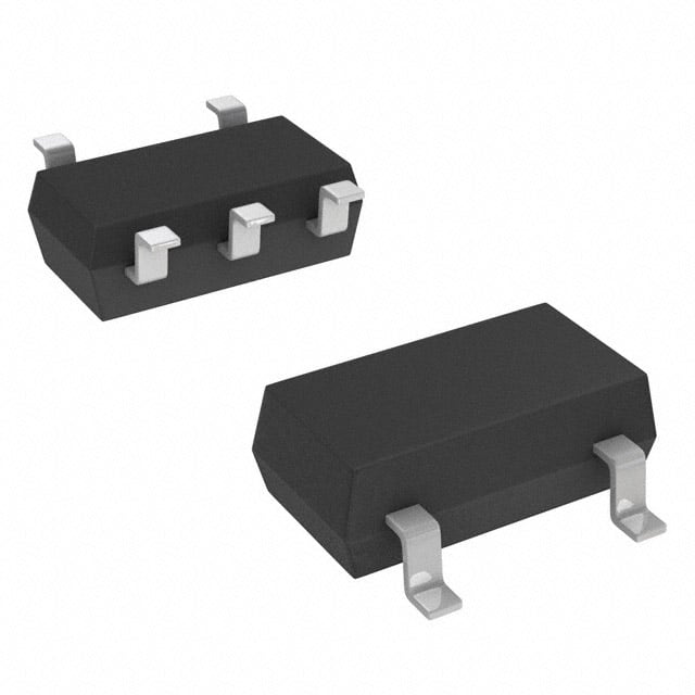
| 描述 | IC OVERVOLTAGE PROTECTOR SC70-5电流和电力监控器、调节器 Signal-Line Over Voltage Protector |
| 产品分类 | |
| 品牌 | Maxim Integrated |
| 产品手册 | |
| 产品图片 |
|
| rohs | 符合RoHS无铅 / 符合限制有害物质指令(RoHS)规范要求 |
| 产品系列 | 电源管理 IC,电流和电力监控器、调节器,Maxim Integrated MAX9940AXK+T- |
| 数据手册 | |
| 产品型号 | MAX9940AXK+T |
| 产品 | Power Monitors |
| 产品培训模块 | http://www.digikey.cn/PTM/IndividualPTM.page?site=cn&lang=zhs&ptm=25703http://www.digikey.cn/PTM/IndividualPTM.page?site=cn&lang=zhs&ptm=25705 |
| 产品目录页面 | |
| 产品种类 | 电流和电力监控器、调节器 |
| 供应商器件封装 | SC-70-5 |
| 其它名称 | MAX9940AXK+TCT |
| 功率(W) | 245mW |
| 包装 | 剪切带 (CT) |
| 商标 | Maxim Integrated |
| 安装风格 | SMD/SMT |
| 封装 | Reel |
| 封装/外壳 | 6-TSSOP(5 引线),SC-88A,SOT-353 |
| 封装/箱体 | SC-70-5 |
| 工作温度范围 | - 40 C to + 125 C |
| 工厂包装数量 | 2500 |
| 应用 | 通用 |
| 应用说明 | |
| 技术 | 混合技术 |
| 标准包装 | 1 |
| 电压-工作 | 5.5V |
| 电压-箝位 | 28V |
| 电源电压-最大 | 5.5 V |
| 电源电压-最小 | 2.2 V |
| 电源电流 | 13 uA |
| 电路数 | 1 |
| 系列 | MAX9940 |
| 输入电压范围 | 2.2 V to 5.5 V |
| 零件号别名 | MAX9940 |


- 商务部:美国ITC正式对集成电路等产品启动337调查
- 曝三星4nm工艺存在良率问题 高通将骁龙8 Gen1或转产台积电
- 太阳诱电将投资9.5亿元在常州建新厂生产MLCC 预计2023年完工
- 英特尔发布欧洲新工厂建设计划 深化IDM 2.0 战略
- 台积电先进制程称霸业界 有大客户加持明年业绩稳了
- 达到5530亿美元!SIA预计今年全球半导体销售额将创下新高
- 英特尔拟将自动驾驶子公司Mobileye上市 估值或超500亿美元
- 三星加码芯片和SET,合并消费电子和移动部门,撤换高东真等 CEO
- 三星电子宣布重大人事变动 还合并消费电子和移动部门
- 海关总署:前11个月进口集成电路产品价值2.52万亿元 增长14.8%

PDF Datasheet 数据手册内容提取
19-4168; Rev 0; 2/09 Signal-Line Overvoltage Protector for Low-Voltage Devices General Description Features M The MAX9940 signal-line overvoltage protector for low- ♦ 28V Protection on EXT A voltage digital communication ports provides protection against high-voltage faults and ESD strikes. The ♦ Extended ESD Protection X MAX9940 is especially useful for sensitive communica- ±4kV IEC 61000-4 Contact on EXT 9 tion protocols such as Maxim 1-Wire® that cannot ♦ +2.2V to +5.5V Supply Voltage Range 9 afford standard means of fault protection, such as large series resistors or large line capacitances. ♦ 13µA Quiescent Supply Current 4 0 The MAX9940 operates from a single supply voltage of ♦ 60ns Fault Reaction Time +2.2V to +5.5V and consumes only 13µA of quiescent ♦ Small, 5-Pin SC70 supply current. The EXT port is protected up to 28V. The device features a reaction time of 60ns for fast ♦ -40°C to +125°C Temperature Range action during fault conditions and operates over the -40°C to +125°C automotive temperature range. Applications Ordering Information Notebook Computers PIN- TOP PART TEMP RANGE Portable Devices PACKAGE MARK Industrial Equipment MAX9940AXK+ -40°C to +125°C 5 SC70 ATC +Denotes a lead(Pb)-free/RoHS-compliant package. 1-Wire is a registered trademark of Maxim Integrated Products, Inc. Block Diagram/Typical Application Circuit NOTEBOOK ADAPTER VDD = 3.3V LOAD NOTEBOOK BATTERY CHARGER ENABLE VCC MAX9940 MICROCONTROLLER + 2kΩ - PROTECTION 20V CIRCUIT 1-Wire DATA DEVICE EXT Rx INT N Rx P Tx Tx GND ________________________________________________________________Maxim Integrated Products 1 For pricing, delivery, and ordering information,please contact Maxim Directat 1-888-629-4642, or visit Maxim’s website at www.maxim-ic.com.
Signal-Line Overvoltage Protector for Low-Voltage Devices 0 ABSOLUTE MAXIMUM RATINGS 4 (All voltages with respect to GND.) Continuous Power Dissipation (TA= +70°C) 9 VCC...........................................................................-0.3V to +6V 5-Pin SC70 (derate 3.1mW/°C above +70°C)..............245mW 9 INT............................................................................-0.3V to +6V Operating Temperature Range.........................-40°C to +125°C EXT.........................................................................-0.3V to +30V Junction Temperature......................................................+150°C X Continuous Input Current into Any Terminal.....................±20mA Storage Temperature Range.............................-65°C to +150°C A M Stresses beyond those listed under “Absolute Maximum Ratings” may cause permanent damage to the device. These are stress ratings only, and functional operation of the device at these or any other conditions beyond those indicated in the operational sections of the specifications is not implied. Exposure to absolute maximum rating conditions for extended periods may affect device reliability. ELECTRICAL CHARACTERISTICS (VCC = +3.3V, RINT_PULLUP = 2kΩ to VDD, VDD = 3.3V, TA = TMIN to TMAX, unless otherwise noted. Typical values are at TA= +25°C.) (Note 1) PARAMETER SYMBOL CONDITIONS MIN TYP MAX UNITS POWER SUPPLY Power-Supply Voltage VCC 2.2 5.5 V Quiescent Supply Current ICC VINT = 0 13 21 µA DC CHARACTERISTICS INT Voltage Range VINT 0 5.5 V EXT Voltage Range VEXT (Note 2) -0.7 +28 V VCC + VCC + VCC + EXT Rising Threshold VTHR V 0.19 0.26 0.30 VCC + VCC + VCC + EXT Falling Threshold VTHF V 0.09 0.13 0.16 SWITCH CHARACTERISTICS On-Resistance RON 0 < VEXT < VCC, IEXT = ±10mA 43.5 77.5 Ω On-Capacitance CON Capacitance to GND 38 pF INT Off-Capacitance COFF Capacitance to GND 27 pF INT Normal Operation Leakage 0 < VINT < VCC, VCC = 5.5V 3 4.2 µA Current (to GND) EXT Normal Operation Leakage 0 < VEXT < VCC, VCC = 5.5V 3 5 µA Current (to GND) INT Fault Leakage Current VINT = 3.3V, VEXT = 28V 2 10 nA EXT Fault Leakage Current VINT = 3.3V, VEXT = 28V 341 510 µA VCC = VDD = 0, 2.2V < VDD < 5.5V, INT Shutdown Leakage Current RINT_PULLUP = 2kΩ to VDD 38 70 µA (to GND) VCC = VDD = 0 1 nA AC CHARACTERISTICS Power-Up Delay Time tPUP 500 µs Fault, VEXT = 10V, RINT_PULLUP = 200Ω 98 200 Fault Reaction Time tOFF Fault, VEXT = 16V, RINT_PULLUP = 200Ω 60 ns Fault Recovery Time tON Fault removed, VEXT < VCC - 0.8V 271 375 ns Note 1: All devices are 100% production tested at TA= +25°C. Specifications over temperature limits are guaranteed by design. Note 2: Minimum EXT voltage of -0.7V is allowed only with a maximum drawn current of 20mA. 2 _______________________________________________________________________________________
Signal-Line Overvoltage Protector for Low-Voltage Devices Typical Operating Characteristics M (VCC= +3.3V, RINT_PULLUP= 2kΩto VDD, VDD= 3.3V, TA= TMINto TMAX, unless otherwise noted.) A X ON-RESISTANCE ON-RESISTANCE TURN-ON/TURN-OFF TIME 9 vs. VCM vs. VCM vs. TEMPERATURE 5600 MAX9940 toc01 5600 TA = +125°C MAX9940 toc02 ns)235000 TURN-ON MAX9940 toc03 940 ΩSISTANCE () 4300 VCC = 2.5VVCC V=C 3C. 3=V 5.5V ΩSISTANCE () 3400 TA = +85°C URN-OFF TIME (125000 ON-RE 20 ON-RE 20 TA = +25°C URN-ON/T100 TURN-OFF 10 10 T 50 EXT = 0 TO 10V SQUARE WAVE TA = -40°C RPULLUP = 200Ω 0 0 0 0 1 2 3 4 5 6 0 0.5 1.0 1.5 2.0 2.5 3.0 3.5 4.0 -50 -25 0 25 50 75 100 125 150 VCM (V) VCM (V) TEMPERATURE (°C) TURN-ON/TURN-OFF TIME SUPPLY CURRENT vs. TEMPERATURE vs. SUPPLY VOLTAGE INSERTION LOSS vs. FREQUENCY TURN-ON/TURN-OFF TIME (ns)112230505000000 TURN-ONESRXPQUTUL =AL RU0PE T =WO 2 A10V60EVΩ MAX9940 toc04 µSUPPLY CURRENT (A)11111113434556.......0055050 TA T=A +=8 +51°C25°C TA = -40T°AC = +25°C MAX9940 toc05 INSERTION LOSS (dB) -----543210123 MAX9940 toc06 50 TURN-OFF 12.5 -6 0 12.0 -7 -50 -25 0 25 50 75 100 125 150 2.0 2.5 3.0 3.5 4.0 4.5 5.0 5.5 6.0 1k 10k 100k 1M 10M 100M TEMPERATURE (°C) SUPPLY VOLTAGE (V) FREQUENCY (Hz) OFF-ISOLATION vs. FREQUENCY FAULT TURN-ON AND RECOVERY TIME 0 -20 MAX9940 toc07 EXT MAX9940 toc08 1V/div dB) -40 N ( O TI LA -60 0 O S F-I OF -80 INT 500mV/div -100 VDD = VCC = 3.3V -120 0 1k 10k 100k 1M 10M 100M TIME (40μs/div) FREQUENCY (Hz) _______________________________________________________________________________________ 3
Signal-Line Overvoltage Protector for Low-Voltage Devices 0 Typical Operating Characteristics (continued) 4 (VCC= +3.3V, RINT_PULLUP= 2kΩto VDD, VDD= 3.3V, TA= TMINto TMAX, unless otherwise noted.) 9 9 X FAULT TURN-ON TIME FAULT RECOVERY TIME A M RPULLUP = 200Ω MAX9940 toc09 EXT RPULLUP = 2kΩ MAX9940 toc10 EXT 5V/div 5V/div 0 0 INT INT 500mV/div 2V/div 0 0 TIME (100ns/div) TIME (100ns/div) FAULT TURN-ON AND RECOVERY TIME FAULT TURN-ON TIME (SCHOTTKY DIODE FROM INT TO VCC) (SCHOTTKY DIODE FROM INT TO VCC) EXT RPULLUP = 2Ω MAX9940 toc11 EXT MAX9940 toc12 5V/div 5V/div 0 0 INT INT 1V/div 1V/div 0 0 TIME (40μs/div) TIME (100ns/div) VTHR AND VTHF VTHR AND VTHF vs. SUPPLY VOLTAGE vs. TEMPERATURE mV)235000 VTHR MAX9940 toc13 mV) 235000 VTHR MAX9940 toc14 D (200 D ( 200 VOLTAGE THRESHO110500 VTHF VOLTAGE THRESHOL 110500 VTHF 50 50 0 0 2.0 2.5 3.0 3.5 4.0 4.5 5.0 5.5 6.0 -50 -25 0 25 50 75 100 125 SUPPLY VOLTAGE (V) TEMPERATURE (°C) 4 _______________________________________________________________________________________
Signal-Line Overvoltage Protector for Low-Voltage Devices Pin Description M PIN NAME FUNCTION A 1 VCC Power Supply. Can be connected to a microcontroller enable input. X 2 GND Ground 9 3 N.C. No Connection. Not internally connected. 9 4 INT Microcontroller I/O Port. Connection to a microcontroller data port. 4 5 EXT External Connector Port. Connection to a 1-Wire device. 0 Detailed Description Block Diagram/Typical Application Circuit. The series switch cell contains circuitry that ensures the pMOS The MAX9940 is a signal-line overvoltage protector for device turns off properly when the voltage at EXT low-voltage devices that provides circuit protection exceeds the supply voltage. The switch can withstand from high-voltage faults and ESD strikes. The device a maximum voltage of 28V at EXT. provides protection in digital communication lines such as 1-Wire and I2C protocols where large series resis- Comparator tance and capacitances cannot be used to provide The MAX9940 features a low-power, high-speed com- protection due to their impact on VIL/VIH levels and parator that is used to turn off the series switch if a communication timing. The MAX9940 includes a series high-voltage condition is detected on EXT. The nominal switch that connects INT to EXT. When a high-voltage hysteresis of the comparator is 128mV (typical). Fault fault condition occurs on EXT, the MAX9940 quickly voltages on EXT that are slightly above VCC trigger the shuts off the series switch and isolates the low-voltage comparator to quickly isolate INT and EXT channels device from the fault condition. In addition to providing from each other. In this mode, the MAX9940 is able to DC fault isolation, the MAX9940 also provides up to withstand 28V on EXT. Negative voltages on EXT are ±4kV IEC 61000-4 contact ESD protection on EXT. The allowed as long as they are current-limited to less than MAX9940 is ideal for circuits that require low-voltage 20mA. devices that communicate to the outside world over connector ports that can expose them to hazardous Typical Application Circuits high-voltage DC faults and ESD strikes. The innovative design of the MAX9940 allows it to with- stand large DC voltages up to 28V at INT and EXT even Series Switch when VCC is 0. This allows application-specific power- The MAX9940 features a series switch to connect a saving and fault-protection schemes to be implemented. low-voltage device such as a microcontroller to an Figures 1 and 2 show two methods of powering the external communication device such as a 1-Wire or I2C MAX9940 from an ENABLE digital output port of the slave. The internal switch is turned off when disabled or microcontroller. Figure 3 shows the conventional method if a fault condition exists, isolating the microcontroller of operating the MAX9940 with both pullup resistor for from any possible damage. The nominal switch resis- digital communication on DATA (RP) and VCC being tance is 38Ω (typ). The series switch is composed of connected directly to VDDof the microcontroller. parallel DMOS and HV-pMOS devices as shown in the ______________________________________________________________________________________________________________________________________________________________________________ 55
Signal-Line Overvoltage Protector for Low-Voltage Devices 0 4 VDD = 3.3V 9 9 X ENABLE A VCC M MICROCONTROLLER 2kRΩ P MAX9940 1-Wire DATA DEVICE Rx Rx INT EXT GND Tx Tx Figure 1. Recommended Scheme for Battery-Operated Devices that Need to Shut Down the MAX9940 and Prevent Power Draw During Short to GND Faults In all three schemes, the MAX9940 protects the micro- operating current of the MAX9940 without any substan- controller from both DC fault voltages above VCC and tial voltage drop (VOH ≈ VDD). By forcing a 0 on the ESD strikes on EXT. The difference in the three ENABLE port of the microcontroller, the MAX9940 can schemes lies in the impact on power consumption in be put into a zero-power mode, thus conserving battery battery-operated devices during normal and short to power. It should be noted that there is no internal ESD GND fault conditions. diode from INT to VCC. This allows the voltage at INT to Figure 1 shows a recommended configuration for battery- stay at VDDeven though VCC= 0, thus drawing no cur- operated devices that need to conserve power both on rent from RP or the battery. However, an internal diode does exist from INT to EXT, and therefore, in the event a continuous basis as well as during short to GND fault of a short to GND fault on EXT, current is drawn through conditions. In this scheme, the ENABLE port of a micro- controller supplies the quiescent current for the RP, causing a power drain from VDD, and can potential- ly reduce battery life. MAX9940 as well as that required for digital communi- cation (i.e., RP pullup resistor). By forcing a 0 on the In Figure 3, VDD powers the MAX9940 directly, and ENABLE digital output port of the microcontroller, the consumes quiescent current on a continuous basis. In MAX9940 is in a zero-power shutdown mode, while also this mode, the internal FET between INT and EXT is preventing any power drain to occur in the event of a kept on as long as the voltage on EXT is below VCC. As short to GND fault on EXT. As stated earlier, EXT main- a result, in the event of a short to GND fault on EXT, tains the ability to withstand DC voltages up to 28V current is drawn through RP, causing a power drain even when VCC= 0. from VDDand potentially reducing battery life. In Figure 2, the ENABLE port of a microcontroller pow- ers the MAX9940. The low 13µA operating current allows standard digital I/O ports to easily supply the 6 _______________________________________________________________________________________
Signal-Line Overvoltage Protector for Low-Voltage Devices M VDD = 3.3V A X 9 ENABLE 9 VCC 4 0 MICROCONTROLLER 2kRΩ P MAX9940 1-Wire DATA DEVICE Rx Rx INT EXT GND Tx Tx Figure 2. Recommended Scheme for Applications that Require the MAX9940 to be Put into Shutdown VDD = 3.3V VCC MICROCONTROLLER 2kRΩ P MAX9940 1-Wire DATA DEVICE Rx Rx INT EXT GND Tx Tx Figure 3. Recommended Operating Circuit for Nonbattery-Operated Applications _______________________________________________________________________________________ 7
Signal-Line Overvoltage Protector for Low-Voltage Devices 0 Pin Configuration Chip Information 4 PROCESS: BiCMOS 9 9 TOP VIEW X + A VCC 1 5 EXT M MAX9940 GND 2 N.C. 3 4 INT SC70 8 _______________________________________________________________________________________
Signal-Line Overvoltage Protector for Low-Voltage Devices Package Information M For the latest package outline information and land patterns, go to www.maxim-ic.com/packages. A PACKAGE TYPE PACKAGE CODE DOCUMENT NO. X 5 SC70 X5-1 21-0076 9 9 S 4 P E L. 0 5 0, 7 C S PACKAGE OUTLINE, 5L SC70 1 21-0076 E 1 Maxim cannot assume responsibility for use of any circuitry other than circuitry entirely embodied in a Maxim product. No circuit patent licenses are implied. Maxim reserves the right to change the circuitry and specifications without notice at any time. Maxim Integrated Products, 120 San Gabriel Drive, Sunnyvale, CA 94086 408-737-7600 _____________________9 © 2009 Maxim Integrated Products Maxim is a registered trademark of Maxim Integrated Products, Inc.