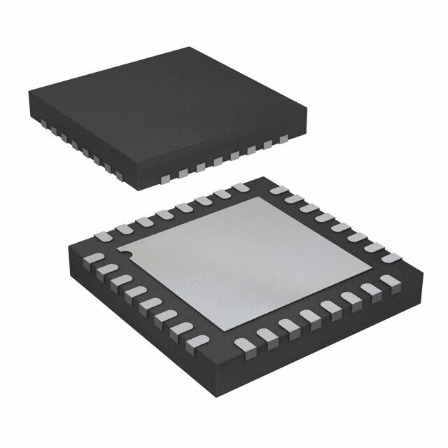
ICGOO在线商城 > 集成电路(IC) > 线性 - 放大器 - 专用 > MAX9001ESD+
- 型号: MAX9001ESD+
- 制造商: Maxim
- 库位|库存: xxxx|xxxx
- 要求:
| 数量阶梯 | 香港交货 | 国内含税 |
| +xxxx | $xxxx | ¥xxxx |
查看当月历史价格
查看今年历史价格
MAX9001ESD+产品简介:
ICGOO电子元器件商城为您提供MAX9001ESD+由Maxim设计生产,在icgoo商城现货销售,并且可以通过原厂、代理商等渠道进行代购。 MAX9001ESD+价格参考。MaximMAX9001ESD+封装/规格:线性 - 放大器 - 专用, Amplifier, Comparator, Reference IC Smart Card 14-SOIC。您可以下载MAX9001ESD+参考资料、Datasheet数据手册功能说明书,资料中有MAX9001ESD+ 详细功能的应用电路图电压和使用方法及教程。
Maxim Integrated的MAX9001ESD+是一款专用线性放大器,属于比较器类别,具有高精度和快速响应特性。该器件广泛应用于需要高速信号检测与电平判别的场景。典型应用包括工业自动化控制系统中的过压/欠压监控、电源管理电路中的电压监测与保护、电池供电设备中的低电量报警等。

MAX9001ESD+内置精密基准电压源和比较器,支持单电源工作,具备优异的抗静电(ESD)能力,适合在电磁干扰较强的环境中稳定运行。其小尺寸封装(如8引脚SOIC)使其适用于空间受限的便携式设备,例如医疗仪器、数据采集系统和通信模块。

此外,该芯片还常用于接口电路中实现电平转换与信号整形,提升系统信号完整性。由于其具备低功耗和高可靠性特点,也适用于汽车电子中的传感器信号处理和安全监控单元。总体而言,MAX9001ESD+适用于对稳定性、精度和响应速度有较高要求的工业、消费类及嵌入式系统应用场景。
| 参数 | 数值 |
| 产品目录 | 集成电路 (IC)半导体 |
| 描述 | IC OP AMP LP HI SPEED 14-SOIC高速运算放大器 Op Amp Comparator Reference IC |
| 产品分类 | |
| 品牌 | Maxim Integrated |
| 产品手册 | |
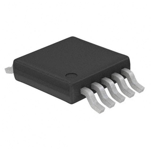
| 产品图片 |
|
| rohs | 符合RoHS无铅 / 符合限制有害物质指令(RoHS)规范要求 |
| 产品系列 | 放大器 IC,高速运算放大器,Maxim Integrated MAX9001ESD+- |
| 数据手册 | |
| 产品型号 | MAX9001ESD+ |
| 产品 | Voltage Feedback Amplifier |
| 产品培训模块 | http://www.digikey.cn/PTM/IndividualPTM.page?site=cn&lang=zhs&ptm=25703http://www.digikey.cn/PTM/IndividualPTM.page?site=cn&lang=zhs&ptm=25705 |
| 产品目录页面 | |
| 产品种类 | 高速运算放大器 |
| 供应商器件封装 | 14-SOIC |
| 共模抑制比—最小值 | 72 dB |
| 包装 | 管件 |
| 商标 | Maxim Integrated |
| 安装类型 | 表面贴装 |
| 安装风格 | SMD/SMT |
| 封装 | Tube |
| 封装/外壳 | 14-SOIC(0.154",3.90mm 宽) |
| 封装/箱体 | SO-14 |
| 工作电源电压 | 2.5 V to 5.5 V |
| 工厂包装数量 | 50 |
| 应用 | 智能卡 |
| 应用说明 | |
| 拓扑结构 | Voltage Feedback |
| 最大工作温度 | + 85 C |
| 最小工作温度 | - 40 C |
| 标准包装 | 50 |
| 电压增益dB | 106 dB |
| 电源电流 | 0.45 mA |
| 类型 | 放大器,比较器,参考 |
| 系列 | MAX9001 |
| 转换速度 | 0.85 V/us |
| 输入补偿电压 | 1.5 mV |
| 通道数量 | 2 Channel |
| 零件号别名 | MAX9001 |


PDF Datasheet 数据手册内容提取
19-0499; Rev 1; 7/98 Low-Power, High-Speed, Single-Supply Op Amp + Comparator + Reference ICs General Description Features M The MAX9000 family features the combination of a high- 'Op Amp + Comparator + Reference in A speed operational amplifier, a 185ns comparator, and a Space-Saving µMAX Package X precision 1.230V reference. These devices operate from a '+2.5V to +5.5V Single-Supply Voltage Range single +2.5V to +5.5V supply and draw less than 500µA of 9 quiescent current. The MAX9001/MAX9004 feature a shut- '340µA Supply Current (MAX9002/MAX9005) 0 down mode that reduces supply current to 2µA and puts 'Unity-Gain Stable (GBW = 1.25MHz) and 0 the outputs into a high-impedance state, making them ideal for portable and battery-powered applications. Decompensated (AV‡ 10V/V, GBW = 8MHz) Options 0 'Op-Amp/Comparator Outputs Swing Rail-to-Rail – The amplifiers in the MAX9000/MAX9001/MAX9002 are M unity-gain stable with a 1.25MHz gain-bandwidth product, 'Ground-Sensing Inputs for Both Op Amp and while the amplifiers in the MAX9003/MAX9004/MAX9005 Comparator A are stable for closed-loop gains of +10V/V or greater with 'Op Amp Stable with Capacitive Loads up to 250pF X an 8MHz gain-bandwidth product. The input common- mode voltage extends from 150mV below the negative 'Internal ±2mV Comparator Hysteresis 9 supply to within 1.2V of the positive supply for the amplifi- 'Fast 185ns Propagation-Delay Comparator 0 er, and to within 1.1V for the comparator. The amplifier and 0 comparator outputs can swing Rail-to-Rail®and deliver up 'No Phase Reversal for Overdriven Inputs 5 to ±2.5mA and ±4.0mA, respectively, to an external load (Both Op Amp and Comparator) while maintaining excellent DC accuracy. The unique 'Internal 1.230V Precision Reference (MAX9000/ design of the comparator output stage substantially MAX9001/MAX9003/MAX9004) reduces switching current during output transitions, virtually ±1% Initial Accuracy eliminating power-supply glitches. Low 8ppm/°C Temperature Drift The comparator’s ±2mV of built-in hysteresis provides Sink or Source up to 1mA noise immunity and prevents oscillations even with a Stable for Capacitive Loads up to 100nF slow-moving input signal. The MAX9000/MAX9001/ MAX9003/MAX9004 have an internal 1.230V ±1% preci- sion reference with a low 8ppm/°C temperature coeffi- Ordering Information cient that can sink or source up to 1mA. The amplifier and PART TEMP. RANGE PIN-PACKAGE reference are stable with capacitive loads up to 250pF and 100nF, respectively. The comparator’s inverting input MAX9000EUA -40°C to +85°C 8 µMAX is internally connected to the reference output in the MAX9000ESA -40°C to +85°C 8 SO MAX9000/MAX9003. MAX9001EUB -40°C to +85°C 10 µMAX ________________________Applications MAX9001ESD -40°C to +85°C 14 SO Single-Supply Zero- Photodiode Preamps Ordering Information continued at end of data sheet. Crossing Detector Smart Card Readers Pin Configurations and Typical Operating Circuit appear at Instruments, Terminals, Infrared Receivers end of data sheet. and Bar-Code Readers for Remote Controls Keyless Entry Sensor Signal Detection Rail-to-Rail is a registered trademark of Nippon Motorola, Ltd. ______________________________________________________________________________Selector Guide INTERNAL OP-AMP GAIN OP-AMPGAIN PART PRECISION STABILITY SHUTDOWN BANDWIDTH PIN-PACKAGE REFERENCE (V/V) (MHz) MAX9000 Yes 1 No 1.25 8 SO/µMAX MAX9001 Yes 1 Yes 1.25 10 µMAX, 14 SO MAX9002 No 1 No 1.25 8 SO/µMAX MAX9003 Yes 10 No 8 8 SO/µMAX MAX9004 Yes 10 Yes 8 10 µMAX, 14 SO MAX9005 No 10 No 8 8 SO/µMAX ________________________________________________________________Maxim Integrated Products 1 For free samples & the latest literature: http://www.maxim-ic.com, or phone 1-800-998-8800. For small orders, phone 408-737-7600 ext. 3468.
Low-Power, High-Speed, Single-Supply Op Amp + Comparator + Reference ICs 5 ABSOLUTE MAXIMUM RATINGS 0 Supply Voltage (VDDto VSS)....................................-0.3V to +6V 10-Pin µMAX (derate 5.6mW/°C above +70°C)............444mW 0 Voltage Inputs (AIN_, CIN_).............(VSS- 0.3V) to (VDD+ 0.3V) 14-Pin SO (derate 8.3mW/°C above +70°C).................667mW 9 Output Short-Circuit Duration (AOUT, COUT, REF)...Continuous Operating Temperature Range to either VSSor VDD MAX900_E _ _...................................................-40°C to +85°C X Continuous Power Dissipation (TA= +70°C) Maximum Junction Temperature.....................................+150°C A 8-Pin SO (derate 5.88mW/°C above +70°C).................471mW Storage Temperature Range.............................-65°C to +160°C 8-Pin µMAX (derate 4.1mW/°C above +70°C)..............330mW Lead Temperature (soldering, 10sec).............................+300°C M Stresses beyond those listed under “Absolute Maximum Ratings” may cause permanent damage to the device. These are stress ratings only, and functional – operation of the device at these or any other conditions beyond those indicated in the operational sections of the specifications is not implied. Exposure to 0 absolute maximum rating conditions for extended periods may affect device reliability. 0 ELECTRICAL CHARACTERISTICS 0 9 (VDD= +2.5V to +5.5V, VSS= 0, SHDN= VDD(MAX9001/MAX9004 only), VCM(OP AMP)= 0, VAOUT= VDD/ 2, VCM(COMP)= 0 (for MAX9001/MAX9002/MAX9004/MAX9005), COUT = low, IOUT(REF)= 0, TA= TMINto TMAX, unless otherwise noted. Typical values are X at VDD= 5V and TA= +25°C.) A PARAMETER SYMBOL CONDITIONS MIN TYP MAX UNITS M Supply Voltage Range VDD Guaranteed by PSRR tests 2.5 5.5 V MAX9000/MAX9001/ VDD= 3V 410 500 µA MAX9003/MAX9004 VDD= 5V 450 550 Supply Current IDD VDD= 3V 340 425 MAX9002/MAX9005 µA VDD= 5V 375 475 Supply Current in I MAX9001/MAX9004 (V = 0) 2 5 µA Shutdown SHDN SHDN Shutdown Input Bias Current IIN(SHDN) MAX9001/MAX9004 (VSHDN= 0 to VDD) 1 2.5 µA Shutdown Logic High VIH(SHDN) 0.7 x VDD V Shutdown Logic Low VIL(SHDN) 0.3 x VDD V OP AMP Input Offset Voltage VOS MAX900_ES_ ±0.5 ±1.5 mV Input Offset Voltage TCVOS MAX900_ES_ ±1 µV/°C Temperature Coefficient Input Bias Current IBIAS AIN+, AIN- ±0.05 ±2 nA Input Offset Current AIN+, AIN- ±0.02 ±1 nA Input Resistance RIN Differential or common mode 1000 MΩ Input Common-Mode CMVR Guaranteed by CMRR test -0.15 VDD- 1.2 V Voltage Range Common-Mode MAX900_ES_, (VSS- 0.15V) ≤VCM≤(VDD- 1.2V), CMRR 72 96 dB Rejection Ratio VDD= 5.5V Power-Supply Rejection PSRR VDD= 2.5V to 5.5V 74 100 dB Ratio Output Resistance AV= 1V/V 0.01 Ω Output Short-Circuit Shorted to VSS 10 mA Current Shorted to VDD 65 DLeisaakbalgeed Mode Output (DISIOABULTED) VSHDN ≤(0.3V x VDD), VAOUT= 0 to VDD ±0.01 ±1 µA 2 _______________________________________________________________________________________
Low-Power, High-Speed, Single-Supply Op Amp + Comparator + Reference ICs ELECTRICAL CHARACTERISTICS (continued) M (VDD= +2.5V to +5.5V, VSS= 0, SHDN= VDD(MAX9001/MAX9004 only), VCM(OP AMP)= 0, VAOUT= VDD/ 2, VCM(COMP)= 0 (for A MAX9001/MAX9002/MAX9004/MAX9005), COUT = low, IOUT(REF)= 0, TA= TMINto TMAX, unless otherwise noted. Typical values are at VDD= 5V and TA= +25°C.) X PARAMETER SYMBOL CONDITIONS MIN TYP MAX UNITS 9 VAOUT = 0.05V to 2.45V, RL= 100kΩ 94 125 0 VDD= 2.5V VAOUT = 0.2V to 2.3V, RL= 1kΩ 84 115 0 Large-Signal Voltage Gain AVOL VAOUT = 0.05V to 5.4V, RL= 100kΩ 94 120 dB 0 VDD= 5.5V VAOUT = 0.25V to 5.2V, RL= 1kΩ 86 106 – M RL = 100kΩ VDD- VOH 1 5 Output Voltage Swing VOL/ VOH œVAIN+- VAIN-œ ‡ 10mV VOL 1 5 mV A RL = 1kΩ VDD- VOH 140 250 X VOL 60 100 9 MAX9000/MAX9001/MAX9002 1.25 0 Gain-Bandwidth Product GBW MHz MAX9003/MAX9004/MAX9005 8 0 MAX9000/MAX9001/MAX9002 75 5 Phase Margin degrees MAX9003/MAX9004/MAX9005 80 MAX9000/MAX9001/MAX9002 30 Gain Margin dB MAX9003/MAX9004/MAX9005 40 MAX9000/MAX9001/ Total Harmonic Distortion f = 10kHz, MAX9002 (AV= 1V/V) 0.009 THD+N VAOUT= 2Vp-p, % plus Noise VDD= 5V MAX9003/MAX9004/ 0.028 MAX9005 (AV= 10V/V) MAX9000/MAX9001/ 0.85 VDD= 5V, MAX9002 (AV= 1V/V) Slew Rate SR V/µs VAOUT= 4V step MAX9003/MAX9004/ 6.0 MAX9005 (AV= 10V/V) MAX9000/MAX9001/ 6.9 VDD= 5V, MAX9002 (AV= 1V/V) Settling Time to within 0.01% µs VAOUT= 4V step MAX9003/MAX9004/ 2.1 MAX9005 (AV= 10V/V) Input Capacitance CIN 2.5 pF Input Noise Voltage Density VNOISE f = 10kHz 36 nV/√Hz Input Noise Current Density INOISE f = 10kHz 1 fA/√Hz Shutdown Delay Time 0.2 µs Enable Delay Time 2 µs Power-On Time 2 µs MAX9000/MAX9001/MAX9002 (AV= 1V/V) 250 Capacitive-Load Stability CLOAD pF MAX9003/MAX9004/MAX9005 (AV= 10V/V) 250 COMPARATOR Input Offset Voltage VOS MAX900_ES_ (Notes 1, 2) ±1 ±2 mV Input Offset Voltage TCVOS MAX900_ES_ ±1 µV/°C Temperature Coefficient Input-Referred Hysteresis VDD= 5V (Notes 2, 3) 4 7 mV _______________________________________________________________________________________ 3
Low-Power, High-Speed, Single-Supply Op Amp + Comparator + Reference ICs 5 ELECTRICAL CHARACTERISTICS (continued) 0 (VDD= +2.5V to +5.5V, VSS= 0, SHDN= VDD(MAX9001/MAX9004 only), VCM(OP AMP)= 0, VAOUT= VDD/ 2, VCM(COMP)= 0 (for 0 MAX9001/MAX9002/MAX9004/MAX9005), COUT = low, IOUT(REF)= 0, TA= TMINto TMAX, unless otherwise noted. Typical values are 9 at VDD= 5V and TA= +25°C.) X PARAMETER SYMBOL CONDITIONS MIN TYP MAX UNITS A Input Bias Current IBIAS 8 80 nA M Input Offset Current IOS MAX9001/MAX9002/MAX9004/MAX9005 ±2 ±15 nA Common-Mode VSS- VDD- – Voltage Range VCM Guaranteed by CMRR test 0.15 1.1 V 0 Common-Mode MAX9001/MAX9002/MAX9004/MAX9005, 0 Rejection Ratio CMRR 0.15V ≤VCM≤(VDD- 1.1V), VDD= 5.5V 72 100 dB 0 Power-Supply Rejection 9 Ratio PSRR VDD= 2.5V to 5.5V 72 100 dB X ISOURCE= 10µA 5 VDD- VOH A (VCIN+- VCIN-) ISOURCE= 4mA 400 M Output Voltage Swing VOL/VOH ‡ 20mV VOL ISINK= 10µA 5 mV ISINK= 4mA 400 Output Short-Circuit 55 mA Current Disabled Mode Output IOUT VSHDN≤(0.3V x VDD), VCOUT= 0 to VDD ±0.01 ±1 µA Leakage (DISABLED) Propagation Delay tPD+, tPD- VOD= 25mV, RL= 10kΩ, CL= 15pF (Note 4) 185 ns Rise/Fall Time tR, tF VDD= 5V, RL= 10kΩ, CL= 15pF (Note 5) 10 ns Shutdown Delay Time 100 ns Enable Delay Time 100 ns Power-On Time 100 ns VOLTAGE REFERENCE (MAX9000/MAX9001/MAX9003/MAX9004) Output Voltage VREF MAX900_ES_, VDD = 5V, TA = +25°C 1.218 1.230 1.242 V Output Voltage TCVREF 8 ppm/°C Temperature Coefficient Line Regulation VDD = 2.5V to 5.5V 20 250 µV/V VDD = 5V, Sourcing 0.15 0.8 mV/mA Load Regulation IOUT= 0 to 1mA Sinking 0.6 2.0 mV/mA Output Short-Circuit Shorted to VSS 6 mA Current Shorted to VDD 10 Disabled Mode Output VSHDN≤(0.3V x VDD), VREF= 0 to VDD ±0.01 ±1 µA Leakage Output Noise 0.1Hz to 10Hz 20 µVp-p Shutdown Delay Time 1 µs Enable Delay Time RL= 100kΩto VSS, VREFwithin 1% 16 µs Power-On Time RL= 100kΩto VSS, VREFwithin 1% 16 µs Capacitive Load Stability 0 to 100 nF Note 1: Comparator Input Offset is defined as the center of the input-referred hysteresis zone. Note 2: Measured at VCM(COMP)= 0 for the MAX9001/MAX9002/MAX9004/MAX9005; or VCM(COMP)= VREF for the MAX9000/MAX9003. Note 3: Input-referred hysteresis is defined as the difference of the trip points required to change comparator output states. Note 4: VODis the overdrive that is beyond the offset and hysteresis-determined trip points. Note 5: Rise and fall times are measured between 10% and 90% at COUT. 4 _______________________________________________________________________________________
Low-Power, High-Speed, Single-Supply Op Amp + Comparator + Reference ICs __________________________________________Typical Operating Characteristics M (VDD= +5V, VSS= 0, VCM(op amp) = 0, SHDN= VDD, COUT = low, RL= ¥ , TA= +25°C, unless otherwise noted.) A X SUPPLY CURRENT SHUTDOWN SUPPLY CURRENT SHUTDOWN LOGIC THRESHOLD 9 vs. SUPPLY VOLTAGE vs. SUPPLY VOLTAGE vs. SUPPLY VOLTAGE 0 mSUPPLY CURRENT (A) 343450055000000 MAXM90A0X09/M00A2X/M90A0X19/M00A5X9003/MAX9004 MAX9000 TOC01 mDOWN SUPPLY CURRENT (A) 121323......005055 MAX9000 TOC02 DOWN LOGIC THRESHOLD (V) 1122....5005 MAX9000 TOC03 00–MAX9 250 SHUT 0.5 SHUT 0.5 0 0 200 0 0 2.5 3.0 3.5 4.0 4.5 5.0 5.5 2.5 3.0 3.5 4.0 4.5 5.0 5.5 2.5 3.0 3.5 4.0 4.5 5.0 5.5 5 SUPPLY VOLTAGE (V) SUPPLY VOLTAGE (V) SUPPLY VOLTAGE (V) MAX9000/MAX9001/MAX9003/MAX9004 SHUTDOWN SUPPLY CURRENT SHUTDOWN LOGIC THRESHOLD SUPPLY CURRENT vs. TEMPERATURE vs. TEMPERATURE vs. TEMPERATURE mPPLY CURRENT (A) 445050000 VVDDDD == 52..55VV MAX9000 TOC04 mWN SUPPLY CURRENT (A) 2244335.......5050500 VDD = 5.5V MAX9000 TOC05 WN LOGIC THRESHOLD (V)1112....99906480 MAX9000 TOC06 SU DO 1.5 VDD = 2.5V DO 350 HUT 1.0 HUT1.92 S S 0.5 300 0 1.90 -40 -20 0 20 40 60 80 100 -40 -20 0 20 40 60 80 100 -40 -20 0 20 40 60 80 100 TEMPERATURE (°C) TEMPERATURE (°C) TEMPERATURE (°C) MAX9002/MAX9005 OP-AMP OUTPUT VOLTAGE SWING HIGH (VOH) OP-AMP OUTPUT VOLTAGE SWING LOW (VOL) SUPPLY CURRENT vs. TEMPERATURE vs. SOURCE CURRENT vs. SINK CURRENT A) 455000 MAX9000 TOC07 434055000 TA =T A+ 2=5 +°8C5°C MAX9000 TOC08 560000 TA = +85°C MAX9000 TOC09 mY CURRENT ( 400 VDD = 5.5V - V (mV)DOH 223500000 V (mV)OL340000 TA = +25°C PL VD TA = -40°C UP 150 200 S 350 VDD = 2.5V 100 TA = -40°C 100 50 300 0 0 -40 -20 0 20 40 60 80 100 0 1 2 3 4 5 6 0 2 4 6 8 10 12 14 16 18 20 TEMPERATURE (°C) SOURCE CURRENT (mA) SINK CURRENT (mA) _______________________________________________________________________________________ 5
Low-Power, High-Speed, Single-Supply Op Amp + Comparator + Reference ICs 5 ____________________________________Typical Operating Characteristics (continued) 0 (VDD= +5V, VSS= 0, VCM(op amp) = 0, SHDN= VDD, COUT = low, RL= ¥ , TA= +25°C, unless otherwise noted.) 0 9 X CHANGE IN OP-AMP OFFSET VOLTAGE (VOS) CHANGE IN OP-AMP OFFSET VOLTAGE (VOS) OP-AMP COMMON-MODE REJECTION RATIO vs. SUPPLY VOLTAGE vs. TEMPERATURE vs. TEMPERATURE –MA 2300 MAX9000 TOC10 15000 MAX9000 TOC11 999102 MAX9000 TOC12 0 V) 10 V) 900 mCHANGE IN V (OS -100 mCHANGE IN V (OS -500 CMRR (dB) 888879 X 86 -20 -100 A 85 M -30 -150 84 2.5 3.0 3.5 4.0 4.5 5.0 5.5 -40 -20 0 20 40 60 80 100 -40 -20 0 20 40 60 80 100 SUPPLY VOLTAGE (V) TEMPERATURE (°C) TEMPERATURE (°C) OP-AMP LARGE-SIGNAL GAIN OP-AMP LARGE-SIGNAL GAIN OP-AMP LARGE-SIGNAL GAIN vs. OUTPUT VOLTAGE vs. OUTPUT VOLTAGE vs. TEMPERATURE 113400 RVDL DT O= G5.N5VD RL = 100kW MAX9000 TOC13 113400 RL = 100RkLW = 10kW MAX9000 TOC14 113400 RL = 100kW MAX9000 TOC15 GAIN (dB) 112100 RL = 10kW RL = 2kW GAIN (dB) 112100 RL = 2kW GAIN (dB) 112100 RL = 10kW 100 100 100 RL = 1kW 90 90 RVDL DT O= G2.N5VD 90 RVVDLO DUT TO= S V5W.D5DIVN/2G = 0.2V TO 5.3V 80 80 80 0 100 200 300 400 500 600 0 100 200 300 400 500 600 -40 -20 0 20 40 60 80 100 OUTPUT VOLTAGE FROM EITHER SUPPLY (mV) OUTPUT VOLTAGE FROM EITHER SUPPLY (mV) TEMPERATURE (°C) OP-AMP LARGE-SIGNAL GAIN OP-AMP LARGE-SIGNAL GAIN OP-AMP LARGE-SIGNAL GAIN vs. OUTPUT VOLTAGE vs. OUTPUT VOLTAGE vs. TEMPERATURE 113400 RL = 100kW MAX9000 TOC16 140 RVDL DT O= V2.D7DV MAX9000 TOC17 113400 RL = 100kW MAX9000 TOC18 120 RL = 10kW 130 RL = 100kW 120 RL = 10kW AIN (dB) 110 RL = 2kW AIN (dB) 120 RL = 10kW AIN (dB) 110 RL = 1kW G G G 100 RL = 2kW 100 110 90 VDD = 5.5V 90 RVDL DT O= V2.D5DV/2 RL TO VDD VOUT SWING = 0.2V TO 2.3V 80 100 80 0 100 200 300 400 500 600 0 100 200 300 400 500 600 -40 -20 0 20 40 60 80 100 OUTPUT VOLTAGE FROM EITHER SUPPLY (mV) OUTPUT VOLTAGE FROM EITHER SUPPLY (mV) TEMPERATURE (°C) 6 _______________________________________________________________________________________
Low-Power, High-Speed, Single-Supply Op Amp + Comparator + Reference ICs _____________________________Typical Operating Characteristics (continued) M (VDD= +5V, VSS= 0, VCM(op amp) = 0, SHDN= VDD, COUT = low, RL= ¥ , TA= +25°C, unless otherwise noted.) A MAX9000/MAX9001/MAX9002 MAX9000/MAX9001/MAX9002 MAX9000/MAX9001/MAX9002 X OP-AMP GAIN AND PHASE OP-AMP GAIN AND PHASE OP-AMP POWER-SUPPLY REJECTION vs. FREQUENCY (NO LOAD) vs. FREQUENCY (WITH CLOAD) vs. FREQUENCY 9 4600 NAVO =L O+1A0D00 MAX9000 TOC 19 111480408 4600 CAVL == +217000p0F MAX9000 TOC20 111480408 N (dB) -200 NAVO =L O+1AD MAX9000 TOC21 000 GAIN (dB) 200 PHAGSAEIN -70-3732626 PHASE (DEGREES) GAIN (dB) 200 PHAGSAEIN -70-3732626 PHASE (DEGREES) ER-SUPPLY REJECTIO --6400 –MAX W -20 -108 -20 -108 PO -80 9 -144 -144 0 -40 -180 -40 -180 -100 0 100 1k 10k 100k 1M 10M 100 1k 10k 100k 1M 10M 100 1k 10k 100k 1M 10M 5 FREQUENCY (Hz) FREQUENCY (Hz) FREQUENCY (Hz) MAX9003/MAX9004/MAX9005 MAX9003/MAX9004/MAX9005 MAX9003/MAX9004/MAX9005 OP-AMP GAIN AND PHASE OP-AMP GAIN AND PHASE OP-AMP POWER-SUPPLY REJECTION vs. FREQUENCY (NO LOAD) vs. FREQUENCY (WITH CLOAD) vs. FREQUENCY 60 MAX9000 TOC22 180 60 MAX9000 TOC23 180 0 GAIN (dB) 24000 NAVO = L +O1A0D00 PHAGSAEIN -710-137324062648PHASE (DEGREES) GAIN (dB) 24000 CAVL == +217000p0F PHAGSAEIN -710-137324062648 PHASE (DEGREES) ER-SUPPLY REJECTION (dB) ---642000 NAVO = L +O1A0D MAX9000 TOC24 W -20 -108 -20 -108 PO -80 -144 -144 -40 -180 -40 -180 -100 100 1k 10k 100k 1M 10M 100 1k 10k 100k 1M 10M 100 1k 10k 100k 1M 10M FREQUENCY (Hz) FREQUENCY (Hz) FREQUENCY (Hz) MAX9000/MAX9001/MAX9002 MAX9003/MAX9004/MAX9005 OP-AMP PERCENT OVERSHOOT OP-AMP PERCENT OVERSHOOT OP-AMP VOLTAGE NOISE DENSITY vs. LOAD CAPACITANCE vs. LOAD CAPACITANCE vs. FREQUENCY 50 50 1000 40 RAVL T=O + 1VDD/2 RL = 100kW MAX9000 TOC25 40 RAVL T=O + 1V0DDR/L2 = 100kW RL = 10kW MAX9000 TOC26 Hz) 300 MAX9000 TOC27 %) %) (cid:214)V/ OVERSHOOT ( 2300 RL = 10kW RL = 1kW OVERSHOOT ( 2300 TAGE NOISE (n 100 L O 10 10 RL = 1kW V 30 0 0 10 0 100 200 300 400 500 600 700 800 9001000 0 100 200 300 400 500 600 700 800 9001000 1 10 100 1k 10k 100k CLOAD (pF) CLOAD (pF) FREQUENCY (Hz) _______________________________________________________________________________________ 7
Low-Power, High-Speed, Single-Supply Op Amp + Comparator + Reference ICs 5 _____________________________Typical Operating Characteristics (continued) 0 (VDD= +5V, VSS= 0, VCM(op amp) = 0, SHDN= VDD, COUT = low, RL= ¥ , TA= +25°C, unless otherwise noted.) 0 9 MAX9000/MAX9001/MAX9002 MAX9000/MAX9001/MAX9002 OP-AMP TOTAL HARMONIC DISTORTION OP-AMP TOTAL HARMONIC DISTORTION MAX9000/MAX9001/MAX9002 X PLUS NOISE vs. FREQUENCY PLUS NOISE vs. VAOUT OP-AMP OUTPUT IMPEDANCE vs. FREQUENCY A 1 0.25 1k 9000–M THD + NOISE (%) 0.00.11 VA5R0VILN 0 T= =Ok + H2 1VVzD pLD-O/p2WPASS FIRLLT E=R 10RkLW = 1kW MAX9000 TOC28 THD + NOISE (%)000...112050 VA5R0VILN 0 T= k=O H+ 1 1Vz0 DLkDOH/Wz2 SPIANSES W FAIRLVTLE E=R 1kW RL = 10kW MAX9000 TOC29 WTPUT IMPEDANCE () 110010 NAVO = L +O1AD MAX9000 TOC30 X RL = 100kW RL = 100kW OU 0.05 0.1 A M 0.001 0 0.01 10 100 1k 10k 100k 4.0 4.1 4.2 4.3 4.4 4.5 4.6 4.7 4.8 4.9 5.0 100 1k 10k 100k 1M 10M FREQUENCY (Hz) VAOUT SWING (Vp-p) FREQUENCY (Hz) MAX9003/MAX9004/MAX9005 MAX9003/MAX9004/MAX9005 OP-AMP TOTAL HARMONIC DISTORTION OP-AMP TOTAL HARMONIC DISTORTION MAX9003/MAX9004/MAX9005 PLUS NOISE vs. FREQUENCY PLUS NOISE vs. VAOUT OP-AMP OUTPUT IMPEDANCE vs. FREQUENCY 1 VA5R0VILN 0 T= k=O H+ 2 1zV0 0DL0ODm/WV2pP-ApSS FILTER RL = 1kW MAX9000 TOC31 00..2205 VA5R0VILN 0 T= k=O H+ 1 1zV0 0DLkHOD/zW2 SPIANSES W FAILVTEER MAX9000 TOC32 ) 110kk NAVO = L +O1A0D MAX9000 TOC33 THD + NOISE (%) 0.1 VIN VOUTRL = 10RkLW = 100kW THD + NOISE (%)00..1105 VIN 4k36RkL = 1kVRWOLUT WOUTPUT IMPEDANCE ( 10100 RL 0.05 RL = 10kW 1 4k36k RL = 100kW 0.01 0 0.1 10 100 1k 10k 100k 4.0 4.1 4.2 4.3 4.4 4.5 4.6 4.7 4.8 4.9 5.0 100 1k 10k 100k 1M 10M FREQUENCY (Hz) VAOUT SWING (Vp-p) FREQUENCY (Hz) COMPARATOR COMMON-MODE CHANGE IN COMPARATOR OFFSET CHANGE IN COMPARATOR OFFSET REJECTION RATIO (CMRR) VOLTAGE (VOS) vs. SUPPLY VOLTAGE VOLTAGE (VOS) vs. TEMPERATURE vs. TEMPERATURE 125000 MAX9000 TOC34 125000 MAX9000 TOC35 9935 MAX9000 TOC36 100 100 V) V) mANGE IN V (OS -55000 mANGE IN V (OS -55000 CMRR (dB) 9819 H H C C -100 -100 87 -150 -150 -200 -200 85 2.5 3.0 3.5 4.0 4.5 5.0 5.5 -40 -20 0 20 40 60 80 100 -40 -20 0 20 40 60 80 100 SUPPLY VOLTAGE (V) TEMPERATURE (°C) TEMPERATURE (°C) 8 _______________________________________________________________________________________
Low-Power, High-Speed, Single-Supply Op Amp + Comparator + Reference ICs _____________________________Typical Operating Characteristics (continued) M (VDD= +5V, VSS= 0, VCM(op amp) = 0, SHDN= VDD, COUT = low, RL= ¥ , TA= +25°C, unless otherwise noted.) A X COMPARATOR HYSTERESIS COMPARATOR OUTPUT VOLTAGE COMPARATOR OUTPUT VOLTAGE 9 vs. TEMPERATURE SWING HIGH (VOH) vs. SOURCE CURRENT SWING LOW (VOL) vs. SINK CURRENT 0 33..25 MAX9000 TOC37 560000 MAX9000 TOC38 560000 TA = +85°C MAX9000 TOC39 00 mV) V)400 TA = +85°C 400 TA = +25°C –M HYSTERESIS ( 22..96 V - V (mDDOH320000 TA = +25°C V(mV)OL 320000 AX TA = -40°C 9 2.3 TA = -40°C 100 100 0 0 2.0 0 0 -40 -20 0 20 40 60 80 100 0 1 2 3 4 5 6 7 8 9 10 0 1 2 3 4 5 6 7 8 9 10 5 TEMPERATURE (°C) SOURCE CURRENT (mA) SINK CURRENT (mA) COMPARATOR PROPAGATION DELAY POSITIVE COMPARATOR PROPAGATION NEGATIVE COMPARATOR PROPAGATION vs. INPUT OVERDRIVE DELAY (tPD+) vs. LOAD CAPACITANCE DELAY (tPD-) vs. LOAD CAPACITANCE AY (ns)223570050 tPD- MAX9000 TOC40 768000000 OVERDRIVE = 5mV MAX9000 TOC41 768000000 OVERDRIVE = 5mV MAX9000 TOC42 L OVERDRIVE = 25mV GATION DE225 t(ns)PD+ 540000 OVERDRIVE = 100mV t- (ns)PD540000 OVERDRIVE = 25mV A ROP200 tPD+ 300 300 OVERDRIVE = 100mV P 175 200 200 150 100 100 0 10 20 30 40 50 60 70 80 90 100 0 2000 4000 6000 8000 10,000 0 2000 4000 6000 8000 10,000 INPUT OVERDRIVE (mV) CLOAD (pF) CLOAD (pF) COMPARATOR PROPAGATION DELAY VREF POWER-SUPPLY REJECTION VREF OUTPUT VOLTAGE CHANGE vs. TEMPERATURE vs. FREQUENCY vs. TEMPERATURE PROPAGATION DELAY (ns) 111252700550 OVERDRIVE VOLTAGE = 50mV ttPPDD-+ MAX9000 TOC43 POWER-SUPPLY REJECTION (dB) ----462800000 MAX9000 TOC44 VOUTPUT VOLTAGE CHANGE (mV)REF ---11001.....050550 MAX9000TOC45 100 -100 -2.0 -40 -20 0 20 40 60 80 100 1 10 100 1k 10k 100k 1M -40 -20 0 20 40 60 80 100 TEMPERATURE (°C) FREQUENCY (Hz) TEMPERATURE (°C) _______________________________________________________________________________________ 9
Low-Power, High-Speed, Single-Supply Op Amp + Comparator + Reference ICs 5 _____________________________Typical Operating Characteristics (continued) 0 (VDD= +5V, VSS= 0, VCM(op amp) = 0, SHDN= VDD, COUT = low, RL= ¥ , TA= +25°C, unless otherwise noted.) 0 9 X VREF OUTPUT VOLTAGE CHANGE VREF OUTPUT VOLTAGE CHANGE vs. LOAD CURRENT vs. SUPPLY VOLTAGE VREF LOAD-TRANSIENT RESPONSE –MA NGE (mV) 34 MAX9000 TOC46 mNGE (V) 15000 MAX9000 TOC47 2mAI/OdUivT +1mA -1mA MAX9000-TOC48 0 HA 2 SINKING HA C C 0 GE GE A A 0 OLT 1 OLT 0 VREF 9 PUT V 0 SOURCING PUT V 200mV/div X OUT OUT -50 A V REF -1 V REF M -2 -100 -2.0 -1.5 -1.0 -0.5 0 0.5 1.0 1.5 2.0 2.5 3.0 3.5 4.0 4.5 5.0 5.5 50m s/div LOAD CURRENT (mA) SUPPLY VOLTAGE (V) VREF LINE-TRANSIENT RESPONSE VREF 0.1Hz to 10Hz VOLTAGE NOISE COMPARATOR PROPAGATION DELAY 500mVV/dDiDv 5.0V 4.5V MAX9000-TOC49 MAX9000-TOC50 50mVV/dINiv+ VNIONM -LA =OX9 AG00DN0-TDOC51 +50mW -50mW 5m V/div VREF VOUT 100mV/div 2V/div tPD+ tPD- 5m s/div 1sec/div 100ns/div MAX9000/MAX9001/MAX9002 MAX9000/MAX9001/MAX9002 OP-AMP SMALL-SIGNAL TRANSIENT MAX9003/MAX9004/MAX9005 OP-AMP SMALL-SIGNAL TRANSIENT RESPONSE RESPONSE WITH CLOAD OP-AMP SMALL-SIGNAL TRANSIENT RESPONSE VIN NAVO =L O+1AD MAX9000-TOC52 VIN CAVL == +2170pF MAX9000-TOC53 10mV/VdIiNv NAVO =L O+1A0D MAX9000-TOC54 50mV/div 50mV/div VOUT 50mV/div VOUT VOUT 50mV/div 50mV/div 500ns/div 1m s/div 500ns/div 10 ______________________________________________________________________________________
Low-Power, High-Speed, Single-Supply Op Amp + Comparator + Reference ICs _____________________________Typical Operating Characteristics (continued) M (VDD= +5V, VSS= 0, VCM(op amp) = 0, SHDN= VDD, COUT = low, RL= ¥ , TA= +25°C, unless otherwise noted.) A X MAX9003/MAX9004/MAX9005 9 OP-AMP SMALL-SIGNAL TRANSIENT MAX9000/MAX9001/MAX9002 MAX9003/MAX9004/MAX9005 0 RESPONSE WITH CLOAD OP-AMP LARGE-SIGNAL TRANSIENT RESPONSE OP-AMP LARGE-SIGNAL TRANSIENT RESPONSE 0 10mV/VdIiNv CAVL == +2170pF MAX9000-TOC55 5V/VdIiNv NAVO =L O+1AD MAX9000-TOC56 0.5V/VdIiNv NAVO =L O+1A0D MAX9000-TOC57 0–M 4V 5V A X VOUT VOUT VOUT 50mV/div 1V/div 1V/div 9 0 0V 0 5 0V 1m s/div 2m s/div 500ns/div Pin Description PIN MAX9001/MAX9004 NAME FUNCTION MAX9000/ MAX9002/ MAX9003 MAX9005 10 µMAX 14 SO — — 1 2 SHDN Shutdown Logic Input 1 1 2 3 AOUT Op-Amp Output 2 2 3 4 AIN- Inverting Op-Amp Input 3 3 4 5 AIN+ Noninverting Op-Amp Input 4 4 5 6 VSS Negative Supply or Ground 5 — 6 9 REF Internal Reference Output — 5 7 10 CIN- Inverting Comparator Input 6 6 8 11 CIN+ Noninverting Comparator Input 7 7 9 12 COUT Comparator Output 8 8 10 13 VDD Positive Supply — — — 1, 7, 8, 14 N.C. No Connection. Not internally connected. ______________________________________________________________________________________ 11
Low-Power, High-Speed, Single-Supply Op Amp + Comparator + Reference ICs 5 _______________Detailed Description 0 The MAX9001–MAX9005 are combinations of a high- 0 speed operational amplifier, a 185ns comparator, and a 9 1%-accurate, 8ppm/°C, 1.230V reference. The devices X 1 AOUT OP AMP MMAAXX99000003 VDD 8 aargee os.f feTrheed cino msppaacrea-tosar’vsi ningv 8e-rptining a inndp u1t0 i-sp iinn tµeMrnAaXlly p caocnk-- A nected to the reference output in the MAX9000/MAX9003. M 2 AIN- COUT 7 The MAX9002/MAX9005 do not have an internal refer- COMP ence, but the inverting input of the comparator is avail- – able externally. The MAX9001/MAX9004 include both the 0 3 AIN+ CIN+ 6 inverting input and the reference output. The MAX9000/ 0 MAX9001/MAX9003/MAX9004 typically consume only 0 REF 410µA of quiescent current, while the MAX9002/ 4 VSS REF 5 9 MAX9004 typically consume 340µA. These low-power, X Rail-to-Rail devices provide excellent AC and DC perfor- mance and are ideally suited to operate from a single A supply. The MAX9001/MAX9004 feature a shutdown M mode that sets the outputs in a high-impedance state and reduces the supply current to 2µA, making these devices ideal for portable and battery-powered systems. MAX9002 1 AOUT OP AMP MAX9005 VDD 8 Op Amp The op amps in the MAX9000/MAX9001/MAX9002 are 2 AIN- COUT 7 COMP unity-gain stable with a gain-bandwidth product of 1.25MHz and a slew rate of 0.85V/µs. The amplifiers in the MAX9003/MAX9004/MAX9005 are stable at closed- 3 AIN+ CIN+ 6 loop gains greater than or equal to 10V/V, with a gain- bandwidth product of 8MHz and a slew rate of 6.0V/µs. 4 VSS CIN- 5 The common-mode input voltage range extends from 150mV below the negative rail to within 1.2V of the pos- itive rail. The amplifier output does not undergo phase reversal when the common-mode input range is exceeded, and the input impedance is relatively con- 2 SHDN VDD 13 stant for input voltages within both supply rails. The MOS differential inputs of the amplifiers feature 4M NORMAL/SHUTDOWN CONTROL extremely high input impedance and ultra-low input bias currents. The CMOS output stage achieves true rail-to-rail operation; the outputs swing to within a few 3 AOUT VDD 12 millivolts of the supply rails, thus extending the dynamic OP AMP COMP range. A proprietary design achieves high open-loop gain, enabling these devices to operate at low quies- 4 AIN- CIN+ 11 cent currents yet maintain excellent DC and AC char- acteristics under various load conditions. These 5 AIN+ CIN- 10 devices have been designed to maintain low offset volt- 6 VSS MAX9001 REF REF 9 age over the entire operating-temperature, common- MAX9004 mode, and supply-voltage ranges. Figure 1. MAX9000–MAX90005 Functional Diagrams 12 ______________________________________________________________________________________
Low-Power, High-Speed, Single-Supply Op Amp + Comparator + Reference ICs Comparator amplifier’s output, add a 1µF to 10µF power-supply M The common-mode input range extends from 150mV bypass capacitor. below the negative rail to within 1.1V of the positive rail. A The device has a high degree of isolation between the The bipolar differential inputs of the comparator feature various blocks. To maintain isolation, careful layout is X high input impedance and low input bias currents. The required. Take special precautions to avoid crossing 9 comparators are designed to maintain low offset volt- signal traces, especially from the outputs to the inputs. 0 age over the entire operating-temperature, common- For sensitive applications, shielding might be required. mode, and supply-voltage ranges. In the MAX9000/ 0 In addition, stray capacitance may affect the stability MAX9003, the comparator’s inverting input is internally and frequency response of the amplifier. Decrease 0 connected to the reference output. stray capacitance by minimizing lead lengths in the – The CMOS output stage achieves true rail-to-rail opera- board layout, as well as placing external components M tion; the outputs swing to within a few millivolts of the as close to the device as possible. A supply rails. The comparator’s propagation delay is Op-Amp Frequency Stability 185ns and is a function of the overdrive (see Typical X Driving large capacitive loads can cause instability in Operating Characteristics). TTL/CMOS compatibility is 9 most low-power, rail-to-rail output amplifiers. These maintained even with a ±4mA output load. A propri- amplifiers are stable with capacitive loads up to 250pF in 0 etary design of the output stage substantially reduces their minimum gain configuration. Stability with higher 0 the cross-conduction current during output transitions, thereby minimizing power-supply glitches typical of capacitive loads can be improved by adding an isolation 5 resistor in series with the op-amp output, as shown in most comparators. In addition, the comparator’s ±2mV Figure 2. This resistor improves the circuit’s phase mar- of built-in hysteresis provides noise immunity and pre- gin by isolating the load capacitor from the amplifier’s vents unstable outputs even with slow-moving input output. Figures 3 and 4 show the response of the ampli- signals. fier with and without an isolation resistor, respectively. Voltage Reference The total capacitance at the op amp’s inputs (input The 1%-accurate, precision 1.230V internal bandgap capacitance + stray capacitance) along with large-value reference in the MAX9000/MAX9001/MAX9003/ feedback resistors can cause additional poles within the MAX9004 achieves an 8ppm/°C temperature coefficient amplifier’s bandwidth, thus degrading the phase margin. (tempco). The reference can sink or source 1mA of load To compensate for this effect, place a 2pF to 10pF current with excellent load regulation. The output typical- capacitor across the feedback resistor, as shown in ly changes only 60µV for a 3V change in input voltage Figure 5. (line regulation). The reference is stable for capacitive loads up to 100nF. Applications Information The MAX9000–MAX9005 offer excellent performance and low power consumption, and are available in space-saving µMAX packages. The following section provides some practical application guidelines. RS MAX9000 CLOAD Bypassing and Layout MAX9001 The MAX9000–MAX9005 operate from a +2.5V to +5.5V MAX9002 single supply or from ±1.25V to ±2.75V dual supplies. (In the MAX9000/MAX9001/MAX9003/MAX9004, the reference voltage is referred to as VSS.). For single- RS supply operation, bypass the power supply with a CLOAD 0.1µF capacitor. For dual supplies, bypass each supply to ground. Bypass with capacitors as close as possible R to the device to minimize lead inductance and noise. R Use a low-inductance ground plane if possible. A print- MAX9003 ed circuit board with a ground plane is recommended. MAX9004 MAX9005 Avoid using wire-wrap boards, breadboards, or IC sockets. For heavy loads at the comparator’s and/or Figure 2. Isolation Resistors to Drive Capacitive Loads ______________________________________________________________________________________ 13
Low-Power, High-Speed, Single-Supply Op Amp + Comparator + Reference ICs 5 900 50mVVIN/ MAX9000-FIG03 50mVVIN/ MAX9000-FIG04 X div div A M – VOUT VOUT 0 50mV/ 50mV/ 0 div div VDD = +1 CL = 510pF 0 9 2m s/div 2m s/div X Figure 3. MAX9000/MAX9001/MAX9002 Op-Amp Small-Signal Figure 4. MAX9000/MAX9001/MAX9002 Op-Amp Small-Signal A Transient Response with Capacitive Load (CL= 510pF) and Transient Response with Capacitive Load (CL= 510pF) and M Isolation Resistor (RISO= 91Ω) No Isolation Resistor AIN+ R2 AOUT VIN R1 COUT R2 R1 REF 2pF TO 10pF Figure 5. Compensation for Input Capacitance Figure 6. External Hysteresis comparator. The outputs do not undergo phase rever- Reference Bypassing sal when the input common-mode range is exceeded, While the internal reference is stable with capacitive and the input impedance is relatively constant for input loads up to 100nF, it does not require an output capaci- voltages within both supply rails. tor for stability. However, in applications where the load or the supply could experience large step changes, an Comparator Hysteresis output capacitor reduces the amount of overshoot and Built-in ±2mV hysteresis improves the comparator’s improves the circuit’s transient response. noise immunity. It prevents unstable outputs with slow- moving or noisy input signals. If additional hysteresis is Comparator Input Stage required, add positive feedback as shown in Figure 6. The comparator’s input bias current is typically 8nA. To This configuration increases the hysteresis band to reduce the offset error caused by the bias current flow- desired levels, but also increases power consumption ing through the external source impedance, match the and slows down the output response. effective impedance seen by each input. High source impedance together with the comparator’s input capaci- tance can increase the propagation delay through the 14 ______________________________________________________________________________________
Low-Power, High-Speed, Single-Supply Op Amp + Comparator + Reference ICs To add hysteresis, use the following procedure: tive supply without an increase in the SHDN input cur- M Step 1: The device’s input bias current can be as high rent, allowing them to be driven from independent logic as 80nA. To minimize error due to the input bias, circuits powered from a different supply voltage. A choose a value for R2 of 100kΩ (VREF / R2), which However, the logic threshold voltage requirements X allows a current of 12.33µA at the upper trip point. must be met for proper operation. If SHDN is left 9 unconnected, the device defaults to the enabled mode Step 2:Choose the width of the hysteresis band. In this through an internal 4MΩ pull-up to VDD. If SHDN is to 0 example, choose 20mV for the added external hystere- be left unconnected, take proper care to ensure that no 0 sis (VEHYST = 20mV). Total hysteresis = VEHYST + signals are coupled to this pin, as this may cause false 0 VIHYST= 24mV. triggering. – R1 = R2 (VEHYST- 2VIHYST) / (VDD+ 2VIHYST) In shutdown mode, all outputs are set to a high-imped- M where IHYSTis the device’s internal hysteresis. ance state and the supply current reduces to 2µA. A Step 3:Determine R1. If VDD= 5V, then R1 = 319Ω. Enable times for the op amp, comparator, and refer- ence are 2µs, 100ns, and 16µs, respectively. Shutdown X Step 4: Check the hysteresis trip points. The following delay times for the op amp, comparator, and reference 9 equation represents the upper trip point (VIN(H)): are 200ns, 100ns, and 1µs, respectively (Figure 7). 0 VIN(H)= [(R1 + R2) / R2] (VREF+ VIHYST) = 1.238V ________________Application Circuits 0 The lower trip point is 24mV lower than upper trip point. 5 VIN(L)= 1.238V - 0.024V = 1.214V. Radio Receiver for Alarms and Detectors Comparator Propagation Delay Figure 8’s circuit is useful as a front end for RF alarms. The comparator’s propagation delay is a function of the An unshielded inductor is used with capacitors C1A, input overdrive voltage. Overdrive voltage is measured C1B, and C1C in a resonant circuit to provide frequen- from beyond the edge of the offset and hysteresis- cy selectivity. The op amp from a MAX9003 amplifies determined trip points (see Typical Operating the signal received. The comparator improves noise Characteristicsfor a graph of Propagation Delay vs. immunity, provides a signal-strength threshold, and Input Overdrive). High source impedance coupled with translates the received signal into a pulse train. The the comparator’s input capacitance increases the prop- tuned LC circuit in Figure 8 is set for 300kHz. The lay- agation delay. Large capacitive loads also increase the out and routing of components for the amplifier should propagation delay. be tight to minimize 60Hz interference and crosstalk Shutdown (SSHHDDNN) from the comparator. Metal shielding is recommended Shutdown is active-low enabled. The SHDN input for to prevent RFI from the comparator or digital circuitry the MAX9001/MAX9004 can be taken above the posi- from exciting the receiving antenna. The transmitting 5SVH/DdiNv MAX9000-FIG07 ANTENNA MAX9003 0.1m F VCC = 5V AOUT 0.1m F 2V/div 20k 10M C1A AMP 390pFC1B COUT L1 0.01nF 5V/div 33m H 9.1k C1C 50-100pF 10k COMP VREF 5.1M 1V/div 1.230V REF 5m s/div L 1 x C 1 = ( 2 p1 fC) 2 LMAEYTOAUL TR-FSIE SNHSIIETLIVDEIN AGR EAAD,VISED AV = +1V/V, CAIN+ = 2.5V, CCIN+ = 2.5V Figure 7. Enable/Disable Response of Op Amp, Comparator, Figure 8. Radio Receiver Application and Reference to SHDN ______________________________________________________________________________________ 15
Low-Power, High-Speed, Single-Supply Op Amp + Comparator + Reference ICs 5 antenna can be long parallel wires spaced about 7.2cm 0 apart, with equal but opposite currents. Radio waves from this antenna are detectable when the receiver is 0 9 brought within close proximity, but cancel out at greater VCC = 5V distances. 100kHz, C2 X 5Vp-p 15pF, 5% A Infrared Receiver Front End for NEC R2 Remote Controls and Data Links NEC PH302B 100k, 0.1m F M The circuit in Figure 9 uses the MAX9003 as a PIN pho- SE307-C 4.99k 1% 0– troedcieoidveer .p Trehaem oppli fiaemr pa nids cdoisncfrigimuirneadto ar sf oar Dane lyiniafrnanreisd- 51W R419%1.A9k R1B 15C01pF, AMP 0 noise and eliminates low-frequency interference from 4.99k 5% sunlight, fluorescent lights, etc. This circuit is applica- 1% 0 ble for TV remote controls and low-frequency data links 100k 1.230V COMP 9 up to 200kbps. Carrier frequencies are limited to X around 100kHz, as in the example circuit. Component MAX9003 0.1m F REF layout and routing for the amplifier should be tight to A LAYOUT-SENSITIVE AREA reduce stray capacitance, 60Hz interference, and RFI M from the comparator. Crosstalk from comparator edges 1 distorts the amplifier signal. To minimize this effect, add R1 x C1 = R2 x C2 = a lowpass RC filter to the connection from the reference 2p fC to the op amp’s noninverting input. Signal Conditioning For incoming signals that require filtering, the internal Figure 9. Infrared Receiver Application amplifier provides an opportunity to create an active fil- ter. This may be required for relatively high-speed sig- nals that require adequate filtering of high-speed carrier frequencies, harmonics, and external noise. In addition, the amplifier can be used to amplify the signal prior to digitizing it through the comparator to improve the comparator’s overall output response and improve its noise immunity. 16 ______________________________________________________________________________________
Low-Power, High-Speed, Single-Supply Op Amp + Comparator + Reference ICs Pin Configurations M A X TOP VIEW 9 0 0 AOUT 1 8 VDD SHDN 1 10 VDD N.C. 1 14 N.C. 0 AOUT 2 9 COUT SHDN 2 13 VDD AIN- 2 7 COUT MAX9001 – MAX9000 AIN- 3 MAX9004 8 CIN+ AOUT 3 12 COUT M AIN+ 3 MAX9002 6 CIN+ MAX9003 AIN+ 4 7 CIN- AIN- 4 MAX9001 11 CIN+ MAX9005 MAX9004 A VSS 4 5 REF (CIN-) VSS 5 6 REF AIN+ 5 10 CIN- X SO/m MAX m MAX VSS 6 9 REF 9 N.C. 7 8 N.C. 0 0 SO 5 ( ) ARE FOR THE MAX9002/MAX9005. Typical Operating Circuit 0.1m F VDD AIN+ INPUT OP AMP MAX9000 AIN- MAX9003 AOUT 1M R2 CIN+ COUT COMP R1 REF REF 1.230V VSS ______________________________________________________________________________________ 17
Low-Power, High-Speed, Single-Supply Op Amp + Comparator + Reference ICs 5 Ordering Information (continued) Chip Information 0 PART TEMP. RANGE PIN-PACKAGE 0 TRANSISTOR COUNT: 283 MAX9002EUA -40°C to +85°C 8 µMAX 9 MAX9002ESA -40°C to +85°C 8 SO X MAX9003EUA -40°C to +85°C 8 µMAX A MAX9003ESA -40°C to +85°C 8 SO M MAX9004EUB -40°C to +85°C 10 µMAX – MAX9004ESD -40°C to +85°C 14 SO 0 MAX9005EUA -40°C to +85°C 8 µMAX 0 MAX9005ESA -40°C to +85°C 8 SO 0 9 X A M Package Information D.EPS MAX U 8L 18 ______________________________________________________________________________________
Low-Power, High-Speed, Single-Supply Op Amp + Comparator + Reference ICs Package Information (continued) M S A P E XB. X A M LU 9 0 1 0 0 0 – M A X 9 0 0 5 ______________________________________________________________________________________ 19
Low-Power, High-Speed, Single-Supply Op Amp + Comparator + Reference ICs 5 Package Information (continued) 0 0 9 SOICN.EPS X A M – 0 0 0 9 X A M MMaaxxiimm ccaannnnoott aassssuummee rreessppoonnssiibbiilliittyy ffoorr uussee ooff aannyy cciirrccuuiittrryy ootthheerr tthhaann cciirrccuuiittrryy eennttiirreellyy eemmbbooddiieedd iinn aa MMaaxxiimm pprroodduucctt.. NNoo cciirrccuuiitt ppaatteenntt lliicceennsseess aarree iimmpplliieedd.. MMaaxxiimm rreesseerrvveess tthhee rriigghhtt ttoo cchhaannggee tthhee cciirrccuuiittrryy aanndd ssppeecciiffiiccaattiioonnss wwiitthhoouutt nnoottiiccee aatt aannyy ttiimmee.. 2200 ________________________________________MMaaxxiimm IInntteeggrraatteedd PPrroodduuccttss,, 112200 SSaann GGaabbrriieell DDrriivvee,, SSuunnnnyyvvaallee,, CCAA 9944008866 440088--773377--77660000 ©© 11999988 MMaaxxiimm IInntteeggrraatteedd PPrroodduuccttss PPrriinntteedd UUSSAA iiss aa rreeggiisstteerreedd ttrraaddeemmaarrkk ooff MMaaxxiimm IInntteeggrraatteedd PPrroodduuccttss..
Mouser Electronics Authorized Distributor Click to View Pricing, Inventory, Delivery & Lifecycle Information: M axim Integrated: MAX9000ESA+ MAX9000ESA+T MAX9000EUA+ MAX9000EUA+T MAX9001ESD+ MAX9001ESD+T MAX9001EUB+ MAX9001EUB+T MAX9002ESA+ MAX9002ESA+T MAX9002EUA+ MAX9002EUA+T MAX9003ESA+ MAX9003ESA+T MAX9003EUA+ MAX9003EUA+T MAX9004ESD+ MAX9004ESD+T MAX9004EUB+ MAX9004EUB+T MAX9005ESA+ MAX9005ESA+T MAX9005EUA+ MAX9005EUA+T MAX9000ESA MAX9000ESA-T MAX9000EUA MAX9000EUA-T MAX9001EUB MAX9001EUB-T MAX9002ESA MAX9002ESA-T MAX9002EUA MAX9002EUA-T MAX9003ESA MAX9003ESA-T MAX9003EUA MAX9003EUA-T MAX9004ESD MAX9004ESD-T MAX9004EUB MAX9004EUB-T MAX9005ESA MAX9005ESA-T

 Datasheet下载


