ICGOO在线商城 > 集成电路(IC) > PMIC - 稳压器 - DC DC 开关稳压器 > MAX8646ETG+
- 型号: MAX8646ETG+
- 制造商: Maxim
- 库位|库存: xxxx|xxxx
- 要求:
| 数量阶梯 | 香港交货 | 国内含税 |
| +xxxx | $xxxx | ¥xxxx |
查看当月历史价格
查看今年历史价格
MAX8646ETG+产品简介:
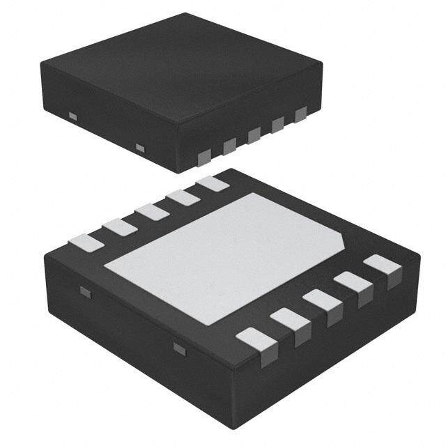
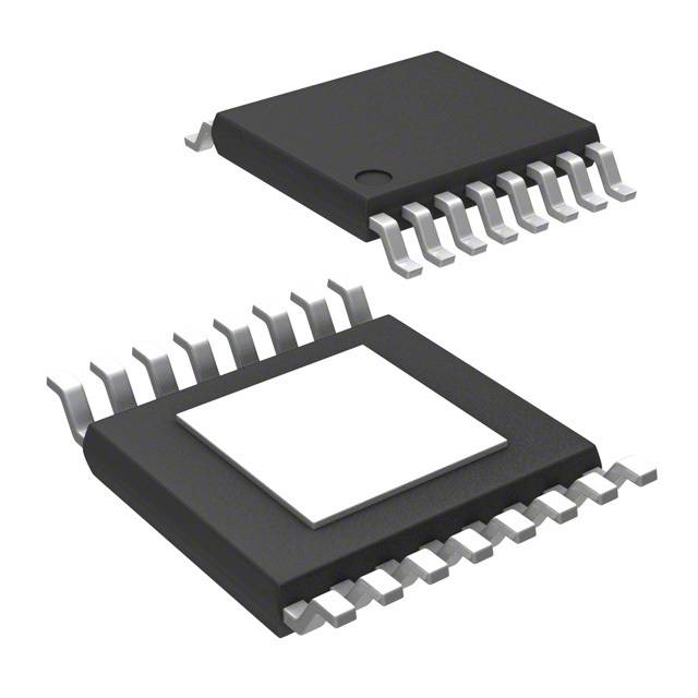
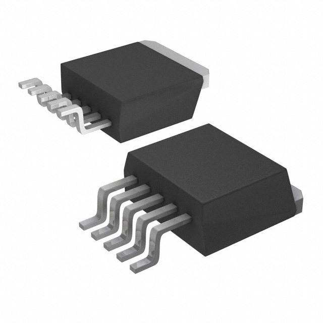
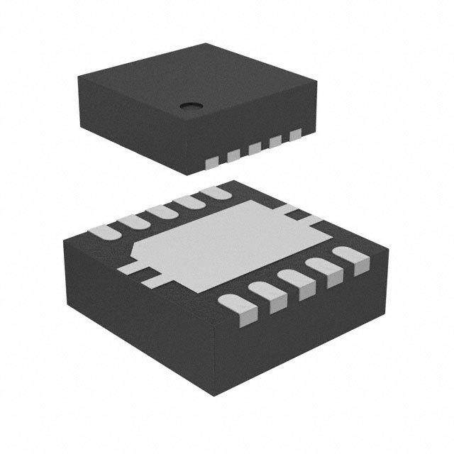
ICGOO电子元器件商城为您提供MAX8646ETG+由Maxim设计生产,在icgoo商城现货销售,并且可以通过原厂、代理商等渠道进行代购。 MAX8646ETG+价格参考。MaximMAX8646ETG+封装/规格:PMIC - 稳压器 - DC DC 开关稳压器, 可调式 降压 开关稳压器 IC 正 0.6V 1 输出 6A 24-WFQFN 裸露焊盘。您可以下载MAX8646ETG+参考资料、Datasheet数据手册功能说明书,资料中有MAX8646ETG+ 详细功能的应用电路图电压和使用方法及教程。
Maxim Integrated的MAX8646ETG+是一款高效、同步整流的DC-DC降压型开关稳压器,广泛应用于需要高效能电源管理的场景。该器件支持宽输入电压范围(2.7V至5.5V),输出电压可调(0.6V至3.3V),并能提供高达1.5A的连续负载电流。

其主要应用场景包括:

1. 便携式电子设备:如智能手机、平板电脑和手持仪器等,适用于电池供电系统中对效率与空间要求较高的场合。
2. 通信设备:用于无线基站、光模块、路由器等设备中的低压差电源转换,提升整体能效。
3. 工业控制系统:如PLC、传感器模块、工业仪表等,提供稳定可靠的电源调节。
4. 计算机外设:如硬盘驱动器、SSD控制器、USB集线器等,满足多电压轨供电需求。
5. 汽车电子系统:在车载导航、娱乐系统及辅助驾驶设备中用于为微处理器和外围电路提供高效电源。

该器件采用小型TDFN封装,具备轻载高效模式、过温保护、过流保护等功能,适合高密度、高可靠性设计需求。
| 参数 | 数值 |
| 产品目录 | 集成电路 (IC) |
| 描述 | IC REG BUCK SYNC ADJ 6A 24TQFN |
| 产品分类 | |
| 品牌 | Maxim Integrated |
| 数据手册 | |
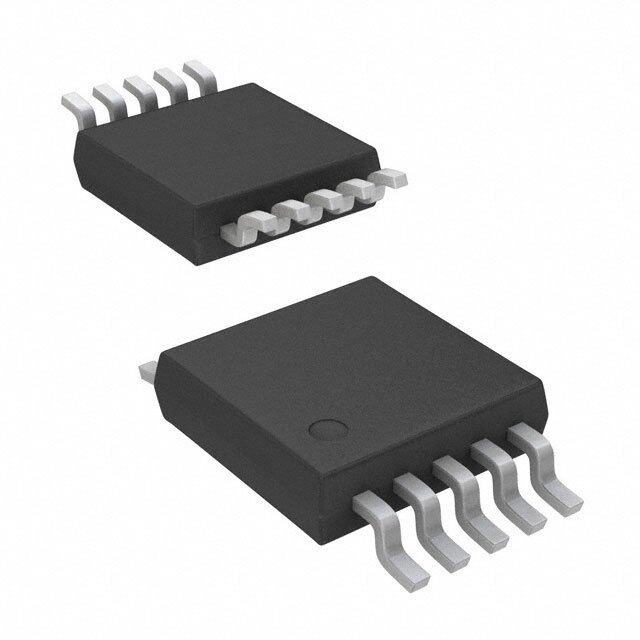
| 产品图片 |
|
| 产品型号 | MAX8646ETG+ |
| PWM类型 | 电压模式 |
| rohs | 无铅 / 符合限制有害物质指令(RoHS)规范要求 |
| 产品系列 | - |
| 产品培训模块 | http://www.digikey.cn/PTM/IndividualPTM.page?site=cn&lang=zhs&ptm=25703http://www.digikey.cn/PTM/IndividualPTM.page?site=cn&lang=zhs&ptm=25705 |
| 供应商器件封装 | 24-TQFN(4x4) |
| 包装 | 管件 |
| 同步整流器 | 是 |
| 安装类型 | 表面贴装 |
| 封装/外壳 | 24-WFQFN 裸露焊盘 |
| 工作温度 | -40°C ~ 85°C |
| 应用说明 | |
| 标准包装 | 1 |
| 电压-输入 | 2.35 V ~ 3.6 V |
| 电压-输出 | 0.6 V ~ 3.2 V |
| 电流-输出 | 6A |
| 类型 | 降压(降压) |
| 输出数 | 1 |
| 输出类型 | 可调式 |
| 频率-开关 | 500kHz ~ 2MHz |




- 商务部:美国ITC正式对集成电路等产品启动337调查
- 曝三星4nm工艺存在良率问题 高通将骁龙8 Gen1或转产台积电
- 太阳诱电将投资9.5亿元在常州建新厂生产MLCC 预计2023年完工
- 英特尔发布欧洲新工厂建设计划 深化IDM 2.0 战略
- 台积电先进制程称霸业界 有大客户加持明年业绩稳了
- 达到5530亿美元!SIA预计今年全球半导体销售额将创下新高
- 英特尔拟将自动驾驶子公司Mobileye上市 估值或超500亿美元
- 三星加码芯片和SET,合并消费电子和移动部门,撤换高东真等 CEO
- 三星电子宣布重大人事变动 还合并消费电子和移动部门
- 海关总署:前11个月进口集成电路产品价值2.52万亿元 增长14.8%


PDF Datasheet 数据手册内容提取
19-3971; Rev 2; 10/07 EVAALVUAAILTAIOBNL EKIT 6A, 2MHz Step-Down Regulator with Integrated Switches General Description Features M The MAX8646 high-efficiency switching regulator deliv- (cid:1) Internal 23mΩRDS(ON)MOSFETs A ers up to 6A load current at output voltages from 0.6V (cid:1) Continuous 6A Output Current X to 0.9 x VIN. The IC operates from 2.35V to 3.6V, mak- (cid:1) ±1% Output Accuracy over Load, Line, ing it ideal for on-board point-of-load and postregula- 8 and Temperature tion applications. Total output error is less than ±1% 6 over load, line, and temperature ranges. (cid:1) Operates from 2.35V to 3.6V Supply 4 The MAX8646 features fixed-frequency PWM mode (cid:1) Adjustable Output from 0.6V to (0.9 x VIN) 6 operation with a switching frequency range of 500kHz (cid:1) Soft-Start Reduces Inrush Supply Current to 2MHz set by an external resistor. High-frequency (cid:1) 500kHz to 2MHz Adjustable Switching Frequency operation allows for an all-ceramic capacitor design. (cid:1) Compatible with Ceramic, Polymer, and The high operating frequency also allows for small-size Electrolytic Output Capacitors external components. (cid:1) VID-Selectable Output Voltages The low-resistance on-chip nMOS switches ensure high 0.6V, 0.7V, 0.8V, 1.0V, 1.2V, 1.5V, 1.8V, 2.0V, efficiency at heavy loads while minimizing critical induc- and 2.5V tances, making the layout a much simpler task with (cid:1) Fully Protected Against Overcurrent and respect to discrete solutions. Following a simple layout Overtemperature and footprint ensures first-pass success in new designs. (cid:1) Safe-Start into Prebiased Output The MAX8646 comes with a high bandwidth (> 14MHz) voltage-error amplifier. The voltage-mode control archi- (cid:1) Sink/Source Current in DDR Applications tecture and the voltage-error amplifier permit a type III (cid:1) Lead-Free, 24-Pin, 4mm x 4mm Thin QFN Package compensation scheme to be utilized to achieve maxi- Ordering Information mum loop bandwidth, up to 20% of the switching fre- quency. High loop bandwidth provides fast transient TEMP PKG response, resulting in less required output capacitance PART PIN-PACKAGE RANGE CODE and allowing for all-ceramic-capacitor designs. 24 Thin QFN-EP* The MAX8646 provides two tri-state logic inputs to MAX8646ETG+ -40°C to +85°C T2444-4 4mm x 4mm select one of nine preset output voltages. The preset output voltages allow customers to achieve ±1% out- +Denotes a lead-free package. put-voltage accuracy without using expensive 0.1% *EP = Exposed pad. resistors. In addition, the output voltage can be set to Typical Operating Circuit any customer value by either using two external resis- tors at the feedback with 0.6V internal reference or applying an external reference voltage to the REFIN INPUT 2.4V, 3.6V input. The MAX8646 offers programmable soft-start IN BST time using one capacitor to reduce input inrush current. MAX8646 OUTPUT The MAX8646 is available in a lead-free, 24-pin, 4mm x EN 1.8V, 6A 4mm, thin QFN package. LX VDD Applications OUT POLs PGND CTL1 ASIC/CPU/DSP Core and I/O Voltages DDR Power Supplies CTL2 FB Base-Station Power Supplies FREQ REFIN Telecom and Networking Power Supplies SS COMP VDD RAID Control Power Supplies PREBIAS PWRGD GND Pin Configuration appears at end of data sheet. ________________________________________________________________Maxim Integrated Products 1 For pricing, delivery, and ordering information, please contact Maxim Direct at 1-888-629-4642, or visit Maxim’s website at www.maxim-ic.com.
6A, 2MHz Step-Down Regulator with Integrated Switches 6 ABSOLUTE MAXIMUM RATINGS 4 IN, VDD, PWRGD to GND......................................-0.3V to +4.5V Continuous Power Dissipation (TA= +70°C) 6 COMP, FB, REFIN, OUT, (derate 27.8mW/°C above +70°C)..........................2222.2mW 8 CTL_, EN, SS, FREQ to GND...................-0.3V to (VDD + 0.3V) Operating Temperature Range...........................-40°C to +85°C LX Current (Note 1).....................................................-8A to +8A Junction Temperature......................................................+150°C X BST to LX..................................................................-0.3V to +4V Storage Temperature Range.............................-65°C to +150°C A PGND to GND.......................................................-0.3V to +0.3V Lead Temperature (soldering, 10s).................................+300°C M Note 1: LX has internal clamp diodes to GND and IN. Applications that forward bias these diodes should take care not to exceed the IC’s package power dissipation limits. Stresses beyond those listed under “Absolute Maximum Ratings” may cause permanent damage to the device. These are stress ratings only, and functional operation of the device at these or any other conditions beyond those indicated in the operational sections of the specifications is not implied. Exposure to absolute maximum rating conditions for extended periods may affect device reliability. ELECTRICAL CHARACTERISTICS (VIN= VDD= 3.3V, VFB= 0.5V, TA= -40°C to +85°C,typical values are at TA= +25°C, circuit of Figure 1, unless otherwise noted.) (Note 2) PARAMETER CONDITIONS MIN TYP MAX UNITS IN/VDD IN and VDD Voltage Range 2.35 3.60 V fS = 1MHz, no load, VIN = 2.5V 4 4.6 IN Supply Current mA (includes gate-drive current) VIN = 3.3V 5.5 VIN = 2.5V 1.4 2.3 VDD Supply Current fS = 1MHz mA VIN = 3.3V 2 Total Shutdown Current from IN VIN = VDD = VBST - VLX = 3.6V, VEN = 0V 13 µA and VDD VDD rising 2 2.1 VDD Undervoltage Lockout V LX starts/stops switching VDD falling 1.8 1.9 Threshold Deglitching 2 µs BST VBST = VDD = VIN = 3.6V, TA = +25°C 5 BST Supply Current µA VLX = 3.6V or 0V, VEN = 0V TA = +85°C 10 PWM COMPARATOR PWM Comparator Propagation 10mV overdrive 20 ns Delay COMP COMP Clamp Voltage, High VIN = 2.35V to 3.6V 2 V COMP Slew Rate 1.4 V/µs PWM Ramp Amplitude 1 V COMP Shutdown Resistance From COMP to GND, VEN = VSS = 0V 8 Ω ERROR AMPLIFIER Select Preset Output-Voltage Accuracy REFIN = SS -1 from +1 % Table 1 FB Regulation Accuracy Using CTL1 = CTL2 = GND 0.594 0.600 0.606 V External Resistors FB to OUT Resistor All VID settings except CTL1 = CTL2 = GND 5 8 11 kΩ Open-Loop Voltage Gain 1kΩ from COMP to GND 115 dB 2 _______________________________________________________________________________________
6A, 2MHz Step-Down Regulator with Integrated Switches ELECTRICAL CHARACTERISTICS (continued) M (VIN= VDD= 3.3V, VFB= 0.5V, TA= -40°C to +85°C,typical values are at TA= +25°C, circuit of Figure 1, unless otherwise noted.) A (Note 2) X PARAMETER CONDITIONS MIN TYP MAX UNITS 8 Error-Amplifier Unity-Gain Parallel 10kΩ, 40pF from COMP to GND (Note 3) 14 26 MHz 6 Bandwidth 4 Error-Amplifier Common-Mode VDD = 2.35V to 2.6V 0 VDD - 1.65 V 6 Input Range VDD = 2.6V to 3.6V 0 VDD - 1.7 Error-Amplifier Minimum Output Sourcing 1000 VCOMP = 1V µA Current Sinking -500 FB Input Bias Current VFB = 0.7, CTL1 = CTL2 = GND, TA = +25°C -200 -40 nA CTL_ VCTL_ = 0V -7 CTL_ Input Bias Current µA VCTL_ = VDD +7 Rising 0.75 High-Z Threshold V Falling VD D - 1.2 Hysteresis All VID transitions 50 mV REFIN REFIN Input Bias Current VREFIN = 0.6V, TA = +25°C -500 -100 nA VDD - VDD = 2.3V to 2.6V 0 1.65 REFIN Common-Mode Range V VDD - VDD = 2.6V to 3.6V 0 1.7 REFIN Offset Voltage CTL1 = CTL2 = GND, TA = +25°C -3 +3 mV LX (All pins combined) LX On-Resistance, High Side ILX = -2A VIN = VBST - VLX = 2.5V 27 mΩ VIN = VBST - VLX = 3.3V 26 45 LX On-Resistance, Low Side ILX = 2A VIN = 2.5V 24 mΩ VIN = 3.3V 23 38 LX Current-Limit Threshold VIN = 2.5V, high-side sourcing 8 11 A VLX = 0V -2 TA = +25°C VLX = 3.6V +2 LX Leakage Current VIN = 3.6V, VEN = VSS = 0V µA VLX = 0V 1 TA = +85°C VLX = 3.6V 1 RFREQ = 50kΩ 0.9 1 1.1 LX Switching Frequency VIN = 2.5V to 3.3V RFREQ = 23.2kΩ 1.8 2 2.2 MHz _______________________________________________________________________________________ 3
6A, 2MHz Step-Down Regulator with Integrated Switches 6 ELECTRICAL CHARACTERISTICS (continued) 4 (VIN= VDD= 3.3V, VFB= 0.5V, TA= -40°C to +85°C,typical values are at TA= +25°C, circuit of Figure 1, unless otherwise noted.) 6 (Note 2) 8 PARAMETER CONDITIONS MIN TYP MAX UNITS X Frequency Range 500 2000 kHz A LX Minimum Off-Time VIN = 2.5V to 3.3V 40 75 ns M LX Maximum Duty Cycle RFREQ = 50kΩ, VIN = 2.5V to 3.3V 93 96 % LX Minimum On-Time RFREQ = 50kΩ, VIN = 2.5V to 3.3V 80 ns RMS LX Output Current 6 A ENABLE EN Input Logic Low, Falling 1.2 0.7 V EN Input Logic High, Rising 1.7 1.4 V EN Hysteresis 200 mV VEN = 0V or 3.6V, TA = +25°C 1 EN, Input Current µA VDD = 3.6V TA = +85°C 0.01 SS SS Charging Current VSS = 0.45V 7 8 9 µA SS Discharge Resistance 500 Ω THERMAL SHUTDOWN Thermal-Shutdown Threshold +165 °C Thermal-Shutdown Hysteresis 20 °C POWER-GOOD (PWRGD) Power-Good Threshold Voltage VFB falling, 3mV hysteresis 87 90 93 % Power-Good Falling Edge Clock 48 Deglitch cycles PWRGD Output Voltage Low IPWRGD = 4mA 0.03 0.15 V PWRGD Leakage Current VDD = VPWRGD = 3.6V, VFB = 0.9V 0.01 µA OVERCURRENT LIMIT Clock Current-Limit Startup Blanking 128 cycles Clock Restart Time 1024 cycles Note 2:Specifications are 100% production tested at TA = +25°C. Limits over the operating temperature range are guaranteed by design and characterization. Note 3:Guaranteed by design. 4 _______________________________________________________________________________________
6A, 2MHz Step-Down Regulator with Integrated Switches Typical Operating Characteristics M (Typical values are: VIN= VDD= 3.3V; VOUT= 1.8V, RFREQ= 50kΩ, IOUT= 6A, and TA = +25°C, unless otherwise noted.) A X 8 EFFICIENCY vs. OUTPUT CURRENT EFFICIENCY vs. OUTPUT CURRENT EFFICIENCY vs. OUTPUT CURRENT 6 19000 MAX8646 toc01 19050 MAX8646 toc02 19050 MAX8646 toc03 46 90 90 80 %) %) 85 %) 85 CIENCY ( 70 VOUT = 1.V8OVUT = 2.5V CIENCY ( 80 VOUT = 1.5V CIENCY ( 80 VOUT = 1.5VVOUT = 1.8V EFFI 60 VOUT = 1.2V EFFI 75 VOUT = 1.8V EFFI 75 70 VOUT = 1.2V 70 VOUT = 1.2V 50 65 65 VIN = 2.5V VIN = VDD = 3.3V VIN = VDD = 2.5V VDD = 3.3V 40 60 60 0.1 1 10 0.1 1 10 0.1 1 10 OUTPUT CURRENT (A) OUTPUT CURRENT (A) OUTPUT CURRENT (A) FREQUENCY vs. INPUT VOLTAGE LOAD REGULATION LOAD TRANSIENT 11890500 - 40°C + 25°C + 85°C MAX8646 toc04 E (%)--00..10005 VOVUINT == V2D.5DV = 3.3V MAX8646 toc05 VOUT VIN = VDD =M A3X.836V46 toc06A50Cm-CVO/dUivPLED FREQUENCY (kHz)111356505000 UT VOLTAGE CHARG---000...221505 VOUT = V1.O8UVT = 1.2V IOUT 1A/div 1200 - 40°C + 25°C + 85°C TP-0.30 U O 1050 -0.35 0A 900 -0.40 2.2 2.6 3.0 3.4 3.8 0 2 4 6 8 40µs/div INPUT VOLTAGE (V) LOAD CURRENT (A) SWITCHING WAVEFORMS SOFT-START WAVEFORM SHUTDOWN WAVEFORMS MAX8646 toc07 MAX8646 toc08 MAX8646 toc09 AC-COUPLED 2V/div VOUT 20mV/div VEN VEN 2V/div 0V 0V 2A/div ILX 0A VOUT 1V/div VLX 1V/div 0V 2V/div VOUT 0V 0V RLOAD = 0.5Ω RLOAD = 0.5Ω 100ns/div 400µs/div 10µs/div _______________________________________________________________________________________ 5
6A, 2MHz Step-Down Regulator with Integrated Switches 6 Typical Operating Characteristics (continued) 4 (Typical values are: VIN= VDD= 3.3V; VOUT= 1.8V, RFREQ= 50kΩ, IOUT= 6A, and TA = +25°C, unless otherwise noted.) 6 8 X INPUT CURRENT vs. INPUT VOLTAGE CURRENT LIMIT vs. OUTPUT VOLTAGE HICCUP CURRENT LIMIT MA 1890 MAX8646 toc10 89 MAX8646 toc11 VOUT MAX8646 toc121V/div 0V µNT (A) 67 MIT (A) 67 NPUT CURRE 345 CURRENT LI 45 IOUT 50AA/div I 2 3 IIN 1 VEN = 0V 1A/div 0 2 0A 2.2 2.4 2.6 2.8 3.0 3.2 3.4 3.6 0.5 1.0 1.5 2.0 2.5 400µs/div INPUT VOLTAGE (V) OUTPUT VOLTAGE (V) RMS INPUT CURRENT DURING SHORT-CIRCUIT EXPOSED PAD TEMPERATURE vs. INPUT VOLTAGE (C4 = 0.022µF) vs. AMBIENT TEMPERATURE FEEDBACK VOLTAGE vs. TEMPERATURE RMS INPUT CURRENT (A)00000000........1223344550505050 MAX8646 toc13 °OSED PAD TEMPERATURE (C) 111456789012000000000 V6AO ULTO =A D1.8V MAX8646 toc14 FEEDBACK VOLTAGE (V)0000000.......55666668901234 MAX8646 toc15 0.10 XP 30 E 0.05 VOUT = 0V 20 MEASURED ON A MAX8646 EV KIT 0.57 0 10 0.56 2.0 2.5 3.0 3.5 4.0 0 20 40 60 80 100 -40 -15 10 35 60 85 INPUT VOLTAGE (V) TEMPERATURE (°C) TEMPERATURE (°C) SOFT-START WITH REFIN STARTING INTO PREBIASED OUTPUT MAX8646 toc16 MAX8646 toc17 2V/div IIN 1A/div VEN 0V 0A VREFIN 0.5V/div VOUT 1V/div 0V 0V VOUT 1V/div 2V/div 0V VPWRGD 0V VPWRGD 2V/div 0V 200µs/div 100µs/div CSS = 6800pF, CO = 122µF, L = 0.56µH, VOUT = 2.5V 6 _______________________________________________________________________________________
6A, 2MHz Step-Down Regulator with Integrated Switches Pin Description M A PIN NAME FUNCTION X Leave Pin Unconnected to Prevent Discharging of Output Capacitor During Soft-Start. Connect to GND 1 PREBIAS otherwise. See the Soft-Starting into a Prebiased Output section. 8 Supply Voltage and Bypass Input. Connect VDD to IN with a 10Ω resistor. Connect a 1µF ceramic 6 2 VDD capacitor from VDD to GND. 4 6 CTL1, Preset Output Voltage Selection Input. CTL1 and CTL2 set the output voltage to one of nine preset 3, 4 CTL2 voltages. See Table 1 for preset voltages. External Reference Input. Connect REFIN to SS to use the internal 0.6V reference. Connecting REFIN to an 5 REFIN external reference voltage forces FB to regulate the voltage applied to REFIN. REFIN is internally pulled to GND when the IC is in shutdown mode. Soft-Start Input. Connect a capacitor from SS to GND to set the startup time. See the Soft-Start and REFIN 6 SS section for details on setting the soft-start time. 7 GND Analog Circuit Ground Output of the Voltage-Error Amplifier. Connect the necessary compensation network from COMP to FB. 8 COMP COMP is internally pulled to GND when the IC is in shutdown mode. Feedback Input. Connect FB to the center tap of an external resistor-divider from the output to GND to set 9 FB the output voltage from 0.6V to 90% of VIN. Connect FB through an RC network to the output when using CTL1 and CTL2 to select any of nine preset voltages. Output Voltage Sense. Connect to the output. Leave OUT unconnected when an external resistor-divider 10 OUT is used. 11 FREQ Oscillator Frequency Selection. Connect a resistor from FREQ to GND to select the switching frequency. P ow er -G ood O utp ut. O pe n- d ra in outp ut that is hig h i mp ed ance wh en VF B ≥ 90% of VR EF IN or 0.6V . PW RGD i s 12 PWRGD i nter nal ly pu ll ed l ow wh en VF B fall s be l ow 90% of it s re g ul ati on po in t. PW RG D i s in ter nall y pu l le d l ow wh en the IC is i n shutdo wn m ode , VD D or V I N is be l ow the UV L O thre shol d, or the IC i s in therm al shutdo w n. 13 BST High-Side MOSFET Driver Supply. Bypass BST to LX with a 0.1µF capacitor. Inductor Connection. All LX pins are internally connected together. Connect all LX pins to the output 14, 15, 16 LX inductor. LX is high impedance when the IC is in shutdown mode. 17–20 PGND Power Ground. Connect all PGND pins externally to the power ground plane. 21, 22, Power-Supply Input. Input supply range is from 2.35V to 3.6V. Bypass with 22µF ceramic capacitance to IN 23 PGND externally. See the Typical Application Circuit. 24 EN Enable Input. Logic input to enable/disable the MAX8646. — EP Exposed Pad. Connect to a large ground plane to optimize thermal performance. _______________________________________________________________________________________ 7
6A, 2MHz Step-Down Regulator with Integrated Switches 6 Block Diagram 4 6 VDD 8 X A M MAX8646 SHUTDOWN UVLO EN CONTROL CIRCUITRY CURRENT-LIMIT COMPARATOR BIAS LX GENERATOR ILIM THRESHOLD BST IN VOLTAGE BST CAPACITOR REFERENCE CHARGING SWITCH SS SOFT-START CONTROL LOGIC LX IN THERMAL SHUTDOWN REFIN PGND OUT ERROR 8kΩ AMPLIFIER PWM COMPARATOR FB PREBIAS CTL1 VID VOLTAGE- CONTROL CTL2 CIRCUITRY 1VP-P FREQ OSCILLATOR COMP SHDN PWRGD FB COMP LOW DETECTOR 0.9 x VREFIN GND 8 _______________________________________________________________________________________
6A, 2MHz Step-Down Regulator with Integrated Switches Typical Application Circuit M A INPUT 2.4V TO 3.6V X IN BST C10 0.1µF 8 22µC6F 0.1µC7F VDD R105Ω MAX8646 0.4L71µH O1.U8TVP, 6UAT 6 LX 4 VDD 6 C5 OUT 1µF 680Cp3F C228µF C0.901µF x2 CTL2 R3 432Ω CTL1 PGND EN FB C2 FREQ 1500pF 3.5R72kΩ REFIN R4 49.9kΩ SS C1 C4 0.022µF 33pF COMP VDD R1 20kΩ PREBIAS PWRGD GND Figure 1. MAX8646 1MHz, All-Ceramic-Capacitor Design with VOUT= 1.8V Detailed Description op-amp voltage-error amplifier works with type III com- pensation to fully utilize the bandwidth of the high-fre- The MAX8646 high-efficiency, voltage-mode switching quency switching to obtain fast transient response. regulator is capable of delivering up to 6A of output Adjustable soft-start time provides flexibilities to mini- current. The MAX8646 provides output voltages from mize input startup inrush current. An open-drain, 0.6V to 0.9 x VIN from 2.35V to 3.6V input supplies, power-good (PWRGD) output goes high when VFB making it ideal for on-board point-of-load applications. reaches 90% of VREFINor 0.54V. The output voltage accuracy is better than ±1% over load, line, and temperature. Controller Function The MAX8646 features a wide switching frequency The controller logic block is the central processor that range, allowing the user to achieve all-ceramic-capacitor determines the duty cycle of the high-side MOSFET designs and fast transient responses (see Figure 1). The under different line, load, and temperature conditions. high operating frequency minimizes the size of external Under normal operation, where the current-limit and components. The MAX8646 is available in a small (4mm temperature protection are not triggered, the controller x 4mm), lead-free, 24-pin thin QFN package. The REFIN logic block takes the output from the PWM comparator function makes the MAX8646 an ideal candidate for and generates the driver signals for both high-side and DDR and tracking power supplies. Using internal low- low-side MOSFETs. The break-before-make logic and RDS(ON)(23mΩ) n-channel MOSFETs for both high- and the timing for charging the bootstrap capacitors are low-side switches maintains high efficiency at both calculated by the controller logic block. The error signal heavy-load and high-switching frequencies. from the voltage-error amplifier is compared with the ramp signal generated by the oscillator at the PWM The MAX8646 employs voltage-mode control architec- comparator and, thus, the required PWM signal is pro- ture with a high bandwidth (> 14MHz) error amplifier. duced. The high-side switch is turned on at the begin- The voltage-mode control architecture allows up to ning of the oscillator cycle and turns off when the ramp 2MHz switching frequency, reducing board area. The _______________________________________________________________________________________ 9
6A, 2MHz Step-Down Regulator with Integrated Switches 6 voltage exceeds the VCOMP signal or the current-limit BST 4 threshold is exceeded. The low-side switch is then The gate-drive voltage for the high-side, n-channel 6 turned on for the remainder of the oscillator cycle. switch is generated by a flying-capacitor boost circuit. The capacitor between BST and LX is charged from the 8 Current Limit VIN supply while the low-side MOSFET is on. When the X The internal, high-side MOSFET has a typical 11A peak low-side MOSFET is switched off, the voltage of the current-limit threshold. When current flowing out of LX A capacitor is stacked above LX to provide the necessary exceeds this limit, the high-side MOSFET turns off and turn-on voltage for the high-side internal MOSFET. M the synchronous rectifier turns on. The synchronous rectifier remains on until the inductor current falls below Frequency Select (FREQ) the low-side current limit. This lowers the duty cycle The switching frequency is resistor programmable from and causes the output voltage to droop until the current 500kHz to 2MHz. Set the switching frequency of the IC limit is no longer exceeded. The MAX8646 uses a hic- with a resistor (RFREQ) connected from FREQ to GND. cup mode to prevent overheating during short-circuit RFREQis calculated as: output conditions. 49.9kΩ 1 During current limit if VFB drops below 420mV and RFREQ = ×( −0.05µs) stays below this level for 12µs or more, the part enters 0.95µs fS hiccup mode. The high-side MOSFET and the synchro- nous rectifier are turned off and both COMP and REFIN where fSis the desired switching frequency in Hz. are internally pulled low. If REFIN and SS are connect- Power-Good Output (PWRGD) ed together, then both are pulled low. The part remains PWRGD is an open-drain output that goes high imped- in this state for 1024 clock cycles and then attempts to ance when VFB is above 0.9 x VREFIN. PWRGD pulls restart for 128 clock cycles. If the fault causing current low when VFB is below 90% of its regulation for at least limit has cleared, the part resumes normal operation. 48 clock cycles. PWRGD is low during shutdown. Otherwise, the part reenters hiccup mode again. Programming the Output Voltage Soft-Start and REFIN (CTL1, CTL2) The MAX8646 utilizes an adjustable soft-start function As shown in Table 1, the output voltage is pin program- to limit inrush current during startup. An 8µA (typ) cur- mable by the logic states of CTL1 and CTL2. CTL1 and rent source charges an external capacitor connected to CTL2 are tri-level inputs: VDD, unconnected, and GND. SS. The soft-start time is adjusted by the value of the The logic states of CTL1 and CTL2 should be pro- external capacitor from SS to GND. The required grammed only before power-up. Once the part is capacitance value is determined as: enabled, CTL1 and CTL2 should not be changed. If the 8µA×t output voltage needs to be reprogrammed, cycle C= SS power or EN and reprogram before enabling. 0.6V where tSSis the required soft-start time in seconds. The MAX8646 also features an external reference input (REFIN). The IC regulates FB to the voltage applied to REFIN. The internal soft-start is not available when using an external reference. A method of soft-start R1 when using an external reference is shown in Figure 2. Connect REFIN to SS to use the internal 0.6V reference. REFIN R2 C MAX8646 Undervoltage Lockout (UVLO) The UVLO circuitry inhibits switching when VDDis below 2V (typ). Once VDD rises above 2V (typ), UVLO clears and the soft-start function activates. A 100mV hysteresis is built in for glitch immunity. Figure 3 is the type III com- pensation network. Figure 2. Typical Soft-Start Implementation with External Reference 10 ______________________________________________________________________________________
6A, 2MHz Step-Down Regulator with Integrated Switches Shutdown Mode Table 1. CTL1 and CTL2 Output Voltage M Drive EN to GND to shut down the IC and reduce quies- Selection cent current to less than 12µA. During shutdown, the LX A is high impedance. Drive EN high to enable the CTL1 CTL2 VOUT (V) X MAX8646. GND GND 0.6 8 Thermal Protection VDD VDD 0.7 6 Thermal-overload protection limits total power dissipation GND Unconnected 0.8 4 in the device. When the junction temperature exceeds TJ GND VDD 1.0 6 = +165°C, a thermal sensor forces the device into shut- Unconnected GND 1.2 down, allowing the die to cool. The thermal sensor turns the device on again after the junction temperature cools Unconnected Unconnected 1.5 by 20°C, causing a pulsed output during continuous Unconnected VDD 1.8 overload conditions. The soft-start sequence begins after VDD GND 2.0 recovery from a thermal-shutdown condition. VDD Unconnected 2.5 Applications Information where the output ripple due to output capacitance, IN and VDDDecoupling ESR, and ESL is: To decrease the noise effects due to the high switching frequency and maximize the output accuracy of V = IP−P the MAX8646, decouple VINwith a 22µF capacitor from RIPPLE(C) 8 xC xf VIN to PGND. Also decouple VDD with a 1µF from VDD OUT S to GND. Place these capacitors as close to the IC as possible. VRIPPLE(ESR) =IP−P xESR Choose an inductor with the folloInwdinugc etqoura tSioenl:ection VRIPPLE(ESL) = IP−P xESL t ON L=fS ×VOVIUNT××L(IVRIN×−IOVUOTU(MTA)X) or: VRIPPLE(ESL) = IP−P xESL t OFF where LIR is the ratio of the inductor ripple current to full or whichever is larger. load current at the minimum duty cycle. Choose LIR The peak inductor current (IP-P) is: between 20% to 40% for best performance and stability. Uthsaet faitns iinn dtuhcet oarl lowttitehd thdeim loewnseiostn sp.o Pssoiwbldee rDeCd rireosnis ftearnrcitee IP−P = VINf−×VOLUT x VVOUT S IN core types are often the best choice for performance. With any core material, the core must be large enough Use these equations for initial capacitor selection. not to saturate at the current limit of the MAX8646. Determine final values by testing a prototype or an evaluation circuit. A smaller ripple current results in less Output-Capacitor Selection output-voltage ripple. Since the inductor ripple current The key selection parameters for the output capacitor are is a factor of the inductor value, the output voltage rip- capacitance, ESR, ESL, and voltage-rating requirements. ple decreases with larger inductance. Use ceramic These affect the overall stability, output ripple voltage, capacitors for low ESR and low ESL at the switching and transient response of the DC-DC converter. The out- frequency of the converter. The ripple voltage due to put ripple occurs due to variations in the charge stored ESL is negligible when using ceramic capacitors. in the output capacitor, the voltage drop due to the capacitor’s ESR, and the voltage drop due to the Load-transient response depends on the selected out- capacitor’s ESL. Calculate the output voltage ripple put capacitance. During a load transient, the output due to the output capacitance, ESR, and ESL: instantly changes by ESR x ∆ILOAD. Before the con- troller can respond, the output deviates further, V =V + RIPPLE RIPPLE(C) depending on the inductor and output capacitor val- V +V ues. After a short time, the controller responds by regu- RIPPLE(ESR) RIPPLE(ESL) ______________________________________________________________________________________ 11
6A, 2MHz Step-Down Regulator with Integrated Switches 6 lating the output voltage back to its predetermined DCR and the internal switch resistance, RDS(ON). A typi- 4 value. The controller response time depends on the cal value for RDS(ON) is 23mΩ. RO is the output load closed-loop bandwidth. A higher bandwidth yields a resistance, which is equal to the rated output voltage 6 faster response time, preventing the output from deviat- divided by the rated output current. ESR is the total 8 ing further from its regulating value. See the Compen- equivalent series resistance of the output filtering capaci- X sation Designsection for more details. tor. If there is more than one output capacitor of the same A type in parallel, the value of the ESR in the above equa- Input-Capacitor Selection tion is equal to that of the ESR of a single output capaci- M The input capacitor reduces the current peaks drawn tor divided by the total number of output capacitors. from the input power supply and reduces switching The high switching frequency range of the MAX8646 noise in the IC. The total input capacitance must be allows the use of ceramic output capacitors. Since the equal or greater than the value given by the following ESR of ceramic capacitors is typically very low, the fre- equation to keep the input-ripple voltage within specs quency of the associated transfer function zero is higher and minimize the high-frequency ripple current being than the unity-gain crossover frequency, fC, and the zero fed back to the input source: cannot be used to compensate for the double pole creat- D xT xI ed by the output filtering inductor and capacitor. The dou- C = S OUT IN_MIN ble pole produces a gain drop of 40dB/decade and a VIN−RIPPLE phase shift of 180°/decade. The error amplifier must com- where VIN-RIPPLE is the maximum allowed input ripple pensate for this gain drop and phase shift to achieve a voltage across the input capacitors and is recommend- stable high-bandwidth closed-loop system. Therefore, ed to be less than 2% of the minimum input voltage. D use type III compensation as shown in Figures 3 and 4. is the duty cycle (VOUT/VIN) and TS is the switching Type III compensation possesses three poles and two period (1/fS). zeros with the first pole, fP1_EA, located at zero frequency The impedance of the input capacitor at the switching (DC). Locations of other poles and zeros of the type III frequency should be less than that of the input source so compensation are given by: high-frequency switching currents do not pass through 1 the input source but are instead shunted through the fZ1_EA= 2π×R1×C1 input capacitor. High source impedance requires high input capacitance. The input capacitor must meet the 1 ripple current requirement imposed by the switching cur- fZ2_EA= 2π×R3×C3 rents. The RMS input ripple current is given by: IRIPPLE=ILOAD× VOUT×(VVIINN−VOUT) fP3_EA=2π×R11×C2 where IRIPPLEis the input RMS ripple current. fP2_EA= 1 2π×R2×C3 Compensation Design The power transfer function consists of one double pole The above equations are based on the assumptions and one zero. The double pole is introduced by the out- that C1>>C2, and R3>>R2, which are true in most put filtering inductor L and the output filtering capacitor applications. Placements of these poles and zeros are CO. The ESR of the output filtering capacitor deter- determined by the frequencies of the double pole and mines the zero. The double pole and zero frequencies ESR zero of the power transfer function. It is also a are given as follows: function of the desired close-loop bandwidth. The fol- 1 lowing section outlines the step-by-step design proce- fP1_LC=fP2_LC= dure to calculate the required compensation 2π x LxCO x⎛⎝⎜RRO++ERSR⎞⎠⎟ coof mthpe oMneAnXt8s6 f4o6r tihse p MroAgXra8m64m6e. dW thoe an pthrees oeut tvpoultt avgoelt,a Rge3 O L is internal to the IC and R4 does not exist (Figure 3b). When externally programming the MAX8646 (Figure 1 f = 3a), the output voltage is determined by: Z_ESR 2π x ESR x C O where RL is equal to the sum of the output inductor’s 12 ______________________________________________________________________________________
6A, 2MHz Step-Down Regulator with Integrated Switches quencies to 80% of the LC double-pole frequency. M Hence: L VOUT A LX R1 = 1 x L xCO x(RO+ESR) X MAX8646 COUT R3 R2 0.8 xC1 RL +RO 8 OUT 6 FB C3 C3= 1 x L xCO x(RO+ESR) 4 CTL1 R1 C1 0.8 xR3 RL +RO 6 CTL2 COMP R4 Setting the second compensation pole, fP2_EA, at C2 fZ_ESRyields: R2=CO x ESR a)EXTERNAL RESISTOR DIVIDER C3 Set the third compensation pole at 1/2 of the switching L VOUT frequency. Calculate C2 as follows: LX COUT C2 = 1 MAX8646 R2 π ×R1× f × 2 S OUT The above equations provide application compensation when the zero-cross frequency is significantly higher R3 than the double-pole frequency. When the zero-cross 8kΩ C3 frequency is near the double-pole frequency, the actual zero-cross frequency is higher than the calculated fre- FB R1 C1 quency. In this case, lowering the value of R1 reduces VOLTAGE CTL1 COMP the zero-cross frequency. Also, set the third pole of the SELECT CTL2 type III compensation close to the switching frequency C2 if the zero-cross frequency is above 200kHz to boost the phase margin. The recommended range for R3 is 2kΩ to 10kΩ. Note that the loop compensation remains b)INTERNAL PRESET VOLTAGES unchanged if only R4’s resistance is altered to set dif- ferent outputs. Figure 3. Type IIICompensation Network Soft-Starting into a Prebiased Output When the PREBIAS pin is left unconnected, the 0.6× R3 R4= MAX8646 is capable of soft-starting up into a prebi- (VOUT − 0.6) ased output without discharging the output capacitor. This type of operation is also termed monotonic start- The zero-cross frequency of the close-loop, fC should up. However, in order to avoid output voltage glitches be between 10% and 20% of the switching frequency, during soft-start it should be ensured that the inductor fS. A higher zero-cross frequency results in faster tran- current is in continuous conduction mode during the sient response. Once fC is chosen, C1 is calculated end of the soft-start period. this is done by satisfying from the following equation: the following equation: 1.5625 xV C1=2 x π xR3 x(1+IRNL)×fC CO×tVSOS ≥ IP2−P R O Due to the underdamped nature of the output LC dou- where CO is the output capacitor, VO is the output volt- ble pole, set the two zero frequencies of the type III age, tSSis the soft-start time set by the soft-start capac- compensation less than the LC double-pole frequency itor CSS, and IP-Pis the peak inductor ripple current (as defined in the Output-Capacitor Selectionsection). to provide adequate phase boost. Set the two zero fre- Depending on the application, one of these parameters may drive the selection of the others. See Starting into ______________________________________________________________________________________ 13
6A, 2MHz Step-Down Regulator with Integrated Switches 6 4) Connect IN, LX, and PGND separately to a large 4 copper area to help cool the IC to further improve 6 COMPENSATION OPEN-LOOP efficiency and long-term reliability. TRANSFER GAIN 8 FUNCTION 5) Ensure all feedback connections are short and THIRD direct. Place the feedback resistors and compensa- X DOUBLE POLE POLE tion components as close to the IC as possible. A 6) Route high-speed switching nodes, such as LX, GAIN (dB) M away from sensitive analog areas (FB, COMP). SECOND POWER-STAGE POLE TRANSFER FUNCTION Pin Configuration FIRST AND SECOND ZEROS TOP VIEW D D Figure 4. Type III Compensation Illustration GN GN X X X ST P P L L L B 18 17 16 15 14 13 Prebiased Outputwaveforms in the Typical Operating Characteristicssection for an example selection of the PGND 19 12 PWRGD above parameters. Connecting the PREBIAS pin to the PGND 20 11 FREQ GND disables the prebias soft-start feature and causes IN 21 10 OUT the MAX8646 to discharge any voltage present on the output capacitors and then commence its soft-start. IN 22 MAX8646 9 FB IN 23 8 COMP PCB Layout Considerations and Thermal Performance EN 24 7 GND + Careful PCB layout is critical to achieve clean and sta- 1 2 3 4 5 6 ble operation. It is highly recommended to duplicate the S D 1 2 N S MAX8646 EV kit layout for optimum performance. If devia- EBIA VD CTL CTL REFI S tion is necessary, follow these guidelines for good PCB PR THIN QFN layout: 1) Connect input and output capacitors to the power ground plane; connect all other capacitors to the sig- nal ground plane. Chip Information 2) Place capacitors on VDD, VIN, and SS as close as possible to the IC and its corresponding pin using PROCESS: BiCMOS direct traces. Keep power ground plane (connected to PGND) and signal ground plane (connected to GND) separate. 3) Keep the high-current paths as short and wide as possible. Keep the path of switching current short and minimize the loop area formed by LX, the out- put capacitors, and the input capacitors. 14 ______________________________________________________________________________________
6A, 2MHz Step-Down Regulator with Integrated Switches Package Information M (The package drawing(s) in this data sheet may not reflect the most current specifications. For the latest package outline information A go to www.maxim-ic.com/packages.) X PS 8 E N. 6 HI 4 T N F 6 Q L 4 2 ______________________________________________________________________________________ 15
6A, 2MHz Step-Down Regulator with Integrated Switches 6 Package Information (continued) 4 (The package drawing(s) in this data sheet may not reflect the most current specifications. For the latest package outline information 6 go to www.maxim-ic.com/packages.) 8 X A M Revision History Pages changed at Rev 1: 1, 5, 6, 7, 10–14 Pages changed at Rev 2: 1, 2, 4, 8, 9, 13, 15, 16 Maxim cannot assume responsibility for use of any circuitry other than circuitry entirely embodied in a Maxim product. No circuit patent licenses are implied. Maxim reserves the right to change the circuitry and specifications without notice at any time. 16 ____________________Maxim Integrated Products, 120 San Gabriel Drive, Sunnyvale, CA 94086 408-737-7600 © 2007 Maxim Integrated Products is a registered trademark of Maxim Integrated Products. Inc.
Mouser Electronics Authorized Distributor Click to View Pricing, Inventory, Delivery & Lifecycle Information: M axim Integrated: MAX8646ETG+ MAX8646ETG+T

 Datasheet下载

