ICGOO在线商城 > 集成电路(IC) > PMIC - 热管理 > MAX6616AEG+

 Datasheet下载
- 型号: MAX6616AEG+
- 制造商: Maxim
- 库位|库存: xxxx|xxxx
- 要求:
| 数量阶梯 | 香港交货 | 国内含税 |
| +xxxx | $xxxx | ¥xxxx |
查看当月历史价格
查看今年历史价格
MAX6616AEG+产品简介:
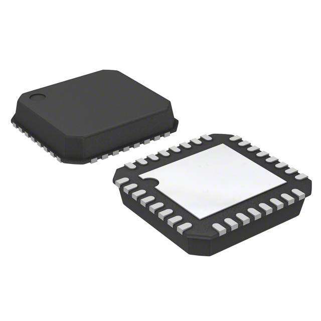
ICGOO电子元器件商城为您提供MAX6616AEG+由Maxim设计生产,在icgoo商城现货销售,并且可以通过原厂、代理商等渠道进行代购。 MAX6616AEG+价格参考¥24.46-¥30.57。MaximMAX6616AEG+封装/规格:PMIC - 热管理, 风扇控制,温度监控器 0°C ~ 140°C 内部和外部 Sensor I²C/SMBus Output 24-QSOP。您可以下载MAX6616AEG+参考资料、Datasheet数据手册功能说明书,资料中有MAX6616AEG+ 详细功能的应用电路图电压和使用方法及教程。
MAX6616AEG+是Maxim Integrated推出的一款热管理专用PMIC(电源管理集成电路),主要应用于需要精确温度监控和风扇控制的电子系统中。其典型应用场景包括工业自动化设备、通信基础设施、网络服务器、存储设备以及高性能计算平台等。

该器件集成了多路温度传感器,可同时监测远程晶体管和本地环境温度,具备高精度测温能力,适用于对散热管理要求较高的系统。MAX6616AEG+还内置风扇转速控制器,支持PWM输出调节风扇速度,实现智能化散热管理,在保障系统稳定运行的同时提升能效、降低噪音。

此外,该芯片提供过温报警和故障保护功能,当检测到温度异常时可及时触发警报或关断机制,有效防止设备因过热损坏。其I²C/SMBus接口便于与主控MCU通信,实现灵活配置和实时监控,适合嵌入式系统和紧凑型设计。

综上所述,MAX6616AEG+广泛用于需高效热管理的工业、通信及计算机领域,是提升系统可靠性和热安全性的理想选择。
| 参数 | 数值 |
| 产品目录 | 集成电路 (IC)热管理产品 |
| 描述 | IC TEMP MON FAN CNTRL 24QSOP板上安装温度传感器 Dual Ch Temperature Monitor |
| 产品分类 | |
| 品牌 | Maxim Integrated |
| 产品手册 | |
| 产品图片 |
|
| rohs | 符合RoHS无铅 / 符合限制有害物质指令(RoHS)规范要求 |
| 产品系列 | 板上安装温度传感器,Maxim Integrated MAX6616AEG+- |
| 数据手册 | |
| 产品型号 | MAX6616AEG+ |
| 产品培训模块 | http://www.digikey.cn/PTM/IndividualPTM.page?site=cn&lang=zhs&ptm=25703http://www.digikey.cn/PTM/IndividualPTM.page?site=cn&lang=zhs&ptm=25705 |
| 产品种类 | 板上安装温度传感器 |
| 传感器类型 | 内部和外部 |
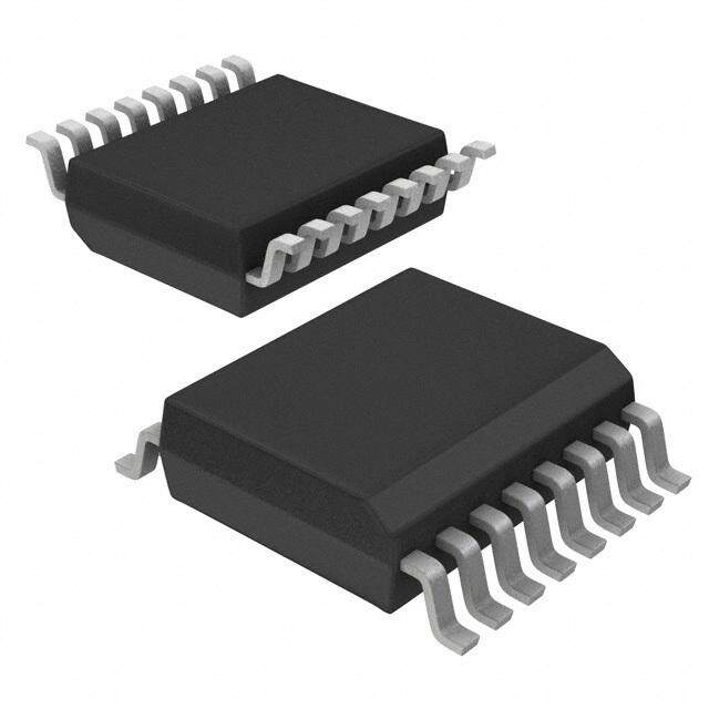
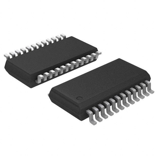
| 供应商器件封装 | 24-QSOP |
| 准确性 | +/- 1 C |
| 功能 | 风扇控制,温度监控器 |
| 包装 | 托盘 |
| 商标 | Maxim Integrated |
| 安装类型 | 表面贴装 |
| 安装风格 | SMD/SMT |
| 封装 | Tube |
| 封装/外壳 | 24-SSOP(0.154",3.90mm 宽) |
| 封装/箱体 | QSOP-24 |
| 工作温度 | -40°C ~ 125°C |
| 工厂包装数量 | 50 |
| 应用说明 | |
| 感应温度 | 0°C ~ 140°C |
| 拓扑 | ADC |
| 数字输出-总线接口 | 2-Wire, I2C, SMBus |
| 最大功率耗散 | 761.9 mW |
| 最大工作温度 | + 125 C |
| 最小工作温度 | - 40 C |
| 标准包装 | 1 |
| 电压-电源 | 3 V ~ 5.5 V |
| 电源电压-最大 | 5.5 V |
| 电源电压-最小 | 3 V |
| 电源电流 | 0.5 mA |
| 精度 | ±4°C 本地(最大), ±1°C 远程(最大) |
| 系列 | MAX6616 |
| 设备功能 | Fan Control, Temperature Monitor |
| 输出报警 | 是 |
| 输出类型 | I²C/SMBus |
| 输出风扇 | 是 |
| 配置 | Local, Remote |
| 零件号别名 | MAX6616 |


- 商务部:美国ITC正式对集成电路等产品启动337调查
- 曝三星4nm工艺存在良率问题 高通将骁龙8 Gen1或转产台积电
- 太阳诱电将投资9.5亿元在常州建新厂生产MLCC 预计2023年完工
- 英特尔发布欧洲新工厂建设计划 深化IDM 2.0 战略
- 台积电先进制程称霸业界 有大客户加持明年业绩稳了
- 达到5530亿美元!SIA预计今年全球半导体销售额将创下新高
- 英特尔拟将自动驾驶子公司Mobileye上市 估值或超500亿美元
- 三星加码芯片和SET,合并消费电子和移动部门,撤换高东真等 CEO
- 三星电子宣布重大人事变动 还合并消费电子和移动部门
- 海关总署:前11个月进口集成电路产品价值2.52万亿元 增长14.8%


PDF Datasheet 数据手册内容提取
19-3713; Rev 2; 10/08 Dual-Channel Temperature Monitors and Fan-Speed Controllers with Thermistor Inputs General Description Features M The MAX6615/MAX6616 monitor two temperature chan- (cid:1) Two Thermistor Inputs A nels, either the internal die temperature and the temper- ature of an external thermistor, or the temperatures of (cid:1) Two Open-Drain PWM Outputs for Fan-Speed X two external thermistors. The temperature data controls Control 6 a PWM output signal to adjust the speed of a cooling (cid:1) Local Temperature Sensor 6 fan, thereby minimizing noise when the system is run- ning cool, but providing maximum cooling when power (cid:1) Six GPIOs (MAX6616) 1 5 dissipation increases. The fans’ tachometer output sig- (cid:1) Programmable Fan-Control Characteristics nfaanls faarileu rme.o nIfi toar efadn b fya tilhuer eM iAs Xd6e6t1e5c/tMedA,X 6th6e1 6F AtoN d_eFtAeIcLt (cid:1) Controlled PWM Rate-of-Change Ensures /M output is asserted. Unobtrusive Fan-Speed Adjustments A The 2-wire serial interface accepts standard system (cid:1) Fail-Safe System Protection X management bus (SMBusTM) write byte, read byte, (cid:1) OTOutput for Throttling or Shutdown 6 send byte, and receive byte commands to read the temperature data and program the alarm thresholds. (cid:1) Nine Different Pin-Programmable SMBus 6 The programmable alarm output can be used to gener- Addresses 1 ate interrupts, throttle signals, or overtemperature shut- (cid:1) 16-Pin and 24-Pin QSOP Packages 6 down signals. The MAX6616 features six GPIOs to provide additional flexibility. All of the GPIOs power-up as inputs, with the exception of GPIO0, which powers up as either an input Ordering Information or an output as determined by connecting the PRESET pin to ground or VCC. PART TEMP RANGE PIN-PACKAGE The MAX6616 is available in a 24-pin QSOP package, MAX6615AEE -40°C to +125°C 16 QSOP while the MAX6615 is available in a 16-pin QSOP pack- MAX6616AEG -40°C to +125°C 24 QSOP age. Both devices operate from a single-supply voltage range of 3.0V to 5.5V, have operating temperature Functional Diagram ranges of -40°C to +125°C, and consume just 500µA of supply current. FAN_FAIL Applications VCC Desktop Computers Servers TH1 TACH1 PWM Power Supplies THERMISTORS GENERATOR PWM1 REF AND LOCAL Networking Equipment TH2 TEMP SENSOR ACNODU NTATCERH PTAWCMH22 Workstations OT SCL SMBus INTERFACE SMBus is a trademark of Intel Corp. AND SDA REGISTERS LOGIC GPIO0* GPIO5* Typical Application Circuits and Pin Configurations appear at end of data sheet. MAX6615 PRESET* MAX6616 GND ADD0 ADD1 *MAX6616 ONLY ________________________________________________________________Maxim Integrated Products 1 For pricing, delivery, and ordering information,please contact Maxim Directat 1-888-629-4642, or visit Maxim’s website at www.maxim-ic.com.
Dual-Channel Temperature Monitors and Fan-Speed Controllers with Thermistor Inputs 6 ABSOLUTE MAXIMUM RATINGS 1 All Voltages Are Referenced to GND Continuous Power Dissipation (TA= +70°C) 6 Supply Voltage (VCC)...............................................-0.3V to +6V 16-Pin QSOP (derated at 8.3mW/°C 6 PWM_, TACH_, OT, FAN_FAIL............................-0.3V to +13.5V above +70°C)............................................................666.7mW ADD0, ADD1, SDA, SCL..........................................-0.3V to +6V 24-Pin QSOP (derated at 9.5mW/°C X All Other Pins..............................................-0.3V to (VCC+ 0.3V) above +70°C)...........................................................761.9 mW A SDA, OT, FAN_FAIL, PWM_, GPIO_ Current....................±50mA ESD Protection (all pins, Human Body Model)....................±2kV TH_ Current........................................................................±1mA Operating Temperature Range.........................-40°C to +125°C M REF Current......................................................................±20mA Junction Temperature......................................................+150°C Storage Temperature Range.............................-65°C to +150°C / 5 Lead Temperature (soldering, 10s).................................+300°C 1 Stresses beyond those listed under “Absolute Maximum Ratings” may cause permanent damage to the device. These are stress ratings only, and functional 6 operation of the device at these or any other conditions beyond those indicated in the operational sections of the specifications is not implied. Exposure to 6 absolute maximum rating conditions for extended periods may affect device reliability. X ELECTRICAL CHARACTERISTICS A (VCC= +3.0V to +5.5V, TA= 0°C to +125°C, unless otherwise noted. Typical values are at VCC= +3.3V, TA= +25°C.) M PARAMETER SYMBOL CONDITIONS MIN TYP MAX UNITS Operating Supply Voltage VCC 3.0 5.5 V Standby Current Interface inactive, ADC in idle state 10 µA Operating Current IS Interface inactive, ADC active 0.5 1 mA VCC = +3.3V, 0.15V ≤ VTH_ ≤ +0.71V (excludes External Temperature Error ±1 °C thermistor errors, thermistor nonlinearity) (Note1) VCC = +3.3V, 0°C ≤ TA ≤ +85°C, ±2.5 Internal Temperature Error °C VCC = +3.3V, 0°C ≤ TA ≤ +125°C ±4 Temperature Resolution 0.125 °C Conversion Time 250 ms Conversion Rate Timing Error -20 +20 % PWM Frequency Error -20 +20 % INPUT/OUTPUT Output Low Voltage VOL VCC = +3V, IOUT = 6mA 0.4 V Output High Leakage Current IOH 1 µA Logic Low Input Voltage VIL 0.8 V Logic High Input Voltage VIH 2.1 V Input Leakage Current 1 µA Input Capacitance CIN 5 pF SMBus TIMING (Figures 2, 3) (Note 2) Serial Clock Frequency fSCLK 10 400 kHz Clock Low Period tLOW 10% to 10% 4 µs Clock High Period tHIGH 90% to 90% 4.7 µs Bus Free Time Between STOP tBUF 4.7 µs and START Conditions SMBus START Condition tSU:STA 90% of SCL to 90% of SDA 4.7 µs Setup Time 2 _______________________________________________________________________________________
Dual-Channel Temperature Monitors and Fan-Speed Controllers with Thermistor Inputs ELECTRICAL CHARACTERISTICS (continued) M (VCC= +3.0V to +5.5V, TA= 0°C to +125°C, unless otherwise noted. Typical values are at VCC= +3.3V, TA= +25°C.) A PARAMETER SYMBOL CONDITIONS MIN TYP MAX UNITS X START Condition Hold Time tHD:STO 10% of SDA to 10% of SCL 4 µs 6 STOP Condition Setup Time tSU:STO 90% of SCL to 10% of SDA 4 µs 6 Data Setup Time tSU:DAT 10% of SDA to 10% of SCL 250 ns 1 Data Hold Time tHD:DAT 10% of SCL to 10% of SDA 300 ns 5 SMBus Fall Time tF 300 ns / M SMBus Rise Time tR 1000 ns SMBus Timeout (Note 3) 29 37 55 ms A Note 1: 1°C of error corresponds to an ADC error of 7.76mV when VREF= 1V. X Note 2: Guaranteed by design and characterization. 6 Note 3: Production tested. 6 1 6 Typical Operating Characteristics (VCC = +3.3V, TA= +25°C, unless otherwise noted.) SUPPLY CURRENT THERMISTOR TEMPERATURE DATA LOCAL TEMPERATURE ERROR vs. SUPPLY VOLTAGE vs. THERMISTOR TEMPERATURE vs. DIE TEMPERATURE µSUPPLY CURRENT (A)110100000 RLOEMCAOLTE SHUTDOWN MAX6615/6 toc01 °MISTOR TEMPERATURE DATA (C)114860200000 MAX6615/6 toc02 °TEMPERATURE ERROR (C) -1012 MAX6615/6 toc03 R E 20 H T 1 0 -2 3.0 3.5 4.0 4.5 5.0 5.5 0 20 40 60 80 100 120 0 25 50 75 100 SUPPLY VOLTAGE (V) THERMISTOR TEMPERATURE (°C) DIE TEMPERATURE (°C) _______________________________________________________________________________________ 3
Dual-Channel Temperature Monitors and Fan-Speed Controllers with Thermistor Inputs 6 Typical Operating Characteristics (continued) 1 (VCC = +3.3V, TA= +25°C, unless otherwise noted.) 6 6 X GPIO SINK CURRENT GPIO OUTPUT VOLTAGE PWM FREQUENCY vs. SUPPLY VOLTAGE vs. GPIO SINK CURRENT vs. DIE TEMPERATURE MA 4550 MAX6615/6 toc04 000...789 MAX6615/6 toc05 345 MAX6615/6 toc06 5/ 40 VGPIO_ = 0.4V 0.6 VCC = 3V T (Hz) 2 661 I (mA)GPIO_ 3305 V (V)GPIO_ 00..45 VCC = 5V UENCY SHIF -101 0.3 EQ X 25 FR -2 0.2 -3 A 20 0.1 -4 NORMALIZED AT TA = +25°C M 15 0 -5 3.0 3.5 4.0 4.5 5.0 5.5 0 10 20 30 40 50 60 70 80 0 25 50 75 100 125 VCC (V) IGPIO_ (mA) DIE TEMPERATURE (°C) PWM FREQUENCY vs. SUPPLY VOLTAGE 0.10 0.08 MAX6615/6 toc07 Hz) 0.06 T ( F HI 0.04 S Y C EN 0.02 U Q E FR 0 -0.02 NORMALIZED AT VCC = 5.0V -0.04 3.0 3.5 4.0 4.5 5.0 5.5 VCC (V) 4 _______________________________________________________________________________________
Dual-Channel Temperature Monitors and Fan-Speed Controllers with Thermistor Inputs Pin Description M PIN A NAME FUNCTION MAX6616 MAX6615 X 1, 2, 5, 20, GPIO0– 6 — Active-Low, Open-Drain GPIOs. Can be pulled up to 5.5V regardless of VCC. 23, 24 GPIO5 6 Fan Driver Output 1. The pullup resistor can be connected to a supply voltage as high as 1 3 1 PWM1 12V, regardless of the supply voltage. See the PWM Output section for configuration. 5 Fan Tachometer Input. Accepts logic-level signal from fan’s tachometer output. Can be / 4 2 TACH1 M connected to a supply voltage as high as 12V, regardless of the supply voltage. 6 3 ADD0 SMBus Slave Address Selection A 7 4 ADD1 SMBus Slave Address Selection X 8 5, 10 GND Ground. Must be connected together for MAX6615. 6 External Thermistor Input 1. Connect a thermistor in series with a fixed resistor between 6 9 6 TH1 REF and ground. 1 10, 15 — N.C. No Connection 6 Reference Voltage Output. Provides 1V during measurements. High impedance when not 11 7 REF measuring. External Thermistor Input 2. Connect a thermistor in series with a fixed resistor between 12 8 TH2 REF and ground. Fan-Failure Output. Asserts low when either fan fails. Can be pulled up as high as 5.5V 13 9 FAN_FAIL regardless of VCC. High impedance when VCC = 0V. 14 — PRESET Connect to GND or VCC to set POR state of the GPIO0. Overtemperature Output. Active low, open drain. Typically used for system shutdown or 16 11 OT clock throttling. Can be pulled up as high as 5.5V regardless of VCC. High impedance when VCC = 0V. 17 12 VCC Power Supply. 3.3V nominal. Bypass with a 0.1µF capacitor to GND. SMBus Serial-Data Input/Output. Pull up with a 10kΩ resistor. Can be pulled up as high 18 13 SDA as 5.5V regardless of VCC. High impedance when VCC = 0V. SMBus Serial-Clock Input. Pull up with a 10kΩ resistor. Can be pulled up as high as 5.5V 19 14 SCL regardless of VCC. High impedance when VCC = 0V. Fan Tachometer Input. Accepts logic-level signal from fan’s tachometer output. Can be 21 15 TACH2 connected to a supply voltage as high as 12V, regardless of the supply voltage. Fan Driver Output 2. The pullup resistor can be connected to a supply voltage as high as 22 16 PWM2 12V, regardless of the supply voltage. See the PWM Output section for configuration. _______________________________________________________________________________________ 5
Dual-Channel Temperature Monitors and Fan-Speed Controllers with Thermistor Inputs 6 WRITE BYTE FORMAT 1 S ADDRESS WR ACK COMMAND ACK DATA ACK P 6 6 — 7 BITS — — 8 BITS — 8 BITS — 1 X SLAVE ADDRESS: EQUIVA- COMMAND BYTE: SELECTS DATA BYTE: DATA GOES INTO THE REG- LENT TO CHIP-SELECT LINE WHICH REGISTER YOU ARE ISTER SET BY THE COMMAND BYTE (TO A OF A 3-WIRE INTERFACE WRITING TO SET THRESHOLDS, CONFIGURATION M MASKS, AND SAMPLING RATE) READ BYTE FORMAT / 5 S ADDRESS WR ACK COMMAND ACK S ADDRESS RD ACK DATA /// P 1 — 7 BITS — — 8 BITS — — 7 BITS — — 8 BITS — — 6 SLAVE ADDRESS: COMMAND BYTE: SLAVE ADDRESS: REPEAT- DATA BYTE: READS 6 EQUIVALENT TO CHIP- SELECTS WHICH ED DUE TO CHANGE IN FROM THE REGISTER X SELECT LINE REGISTER YOU ARE DATA- FLOW DIRECTION SET BY THE COMMAND READING FROM BYTE A SEND BYTE FORMAT RECEIVE BYTE FORMAT M S ADDRESS WR ACK COMMAND ACK P S ADDRESS RD ACK DATA /// P — 7 BITS — — 8 BITS — — — 7 BITS — — 8 BITS — — COMMAND BYTE: SENDS COM- DATA BYTE: READS DATA FROM MAND WITH NO DATA, USUALLY THE REGISTER COMMANDED BY USED FOR ONE-SHOT COMMAND THE LAST READ BYTE OR WRITE BYTE TRANSMISSION; ALSO S = START CONDITION SHADED = SLAVE TRANSMISSION USED FOR SMBUS ALERT RESPONSE RETURN ADDRESS P = STOP CONDITION /// = NOT ACKNOWLEDGED Figure 1. SMBus Protocols Detailed Description have nine different slave addresses available; therefore, a maximum of nine MAX6615/MAX6616 devices can share The MAX6615/MAX6616 accurately monitor two tem- the same bus. perature channels, either the internal die temperature and the temperature of an external thermistor, or the The MAX6615/MAX6616 employ four standard SMBus temperatures of two external thermistors. They report protocols: write byte, read byte, send byte, and receive temperature values in digital form using a 2-wire byte (Figures 1, 2, and 3). The shorter receive byte proto- SMBus/I2C-compatible serial interface. The MAX6615/ col allows quicker transfers, provided that the correct MAX6616 operate from a supply voltage range of 3.0V data register was previously selected by a read byte to 5.5V and consume 500µA (typ) of supply current. instruction. Use caution with the shorter protocols in mul- timaster systems, since a second master could overwrite The temperature data controls the duty cycles of two the command byte without informing the first master. PWM output signals that are used to adjust the speed of a cooling fan. They also feature an overtemperature Temperature data can be read from registers 00h and alarm output to generate interrupts, throttle signals, or 01h. The temperature data format for these registers is shutdown signals. 8 bits, with the LSB representing 1°C (Table 1) and the MSB representing 128°C. The MSB is transmitted first. The MAX6616 also includes six GPIO input/outputs to All values below 0°C clip to 00h. provide additional flexibility. The GPIO0 power-up state is set by connecting the GPIO PRESET input to ground Table 3 details the register address and function, whether or VCC. they can be read or written to, and the power-on reset SMBus Digital Interface From a software perspective, the MAX6615/MAX6616 appear as a set of byte-wide registers. Their devices use a standard SMBus 2-wire/I2C-compatible serial interface to access the internal registers. The MAX6615/MAX6616 6 _______________________________________________________________________________________
Dual-Channel Temperature Monitors and Fan-Speed Controllers with Thermistor Inputs M A B C D E F G H I J K L M tLOW tHIGH A X SMBCLK 6 6 SMBDATA 1 5 tSU:STA tHD:STA tSU:DAT tSU:STO tBUF /M A = START CONDITION E = SLAVE PULLS SMBDATA LINE LOW I = MASTER PULLS DATA LINE LOW B = MSB OF ADDRESS CLOCKED INTO SLAVE F = ACKNOWLEDGE BIT CLOCKED INTO MASTER J = ACKNOWLEDGE CLOCKED INTO SLAVE A C = LSB OF ADDRESS CLOCKED INTO SLAVE G = MSB OF DATA CLOCKED INTO SLAVE K = ACKNOWLEDGE CLOCK PULSE X D = R/W BIT CLOCKED INTO SLAVE H = LSB OF DATA CLOCKED INTO SLAVE L = STOP CONDITION M = NEW START CONDITION 6 6 Figure 2. SMBus Write Timing Diagram 1 6 A B C D E F G H I J K L M tLOW tHIGH SMBCLK SMBDATA tSU:STA tHD:STA tSU:DAT tHD:DAT tSU:STO tBUF A = START CONDITION F = ACKNOWLEDGE BIT CLOCKED INTO MASTER J = ACKNOWLEDGE CLOCKED INTO SLAVE B = MSB OF ADDRESS CLOCKED INTO SLAVE G = MSB OF DATA CLOCKED INTO MASTER K = ACKNOWLEDGE CLOCK PULSE C = LSB OF ADDRESS CLOCKED INTO SLAVE H = LSB OF DATA CLOCKED INTO MASTER L = STOP CONDITION D = R/W BIT CLOCKED INTO SLAVE I = MASTER PULLS DATA LINE LOW M = NEW START CONDITION E = SLAVE PULLS SMBDATA LINE LOW Figure 3. SMBus Read Timing Diagram (POR) state. See Tables 3–7 for all other register functions 0°, the value in the corresponding temperature register and the Register Descriptionssection. is clipped to zero when a negative offset is pro- grammed into the thermistor offset register (17h). Temperature Measurements Local (internal) temperature data is expressed directly The averaging ADC integrates over a 120ms period in degrees Celsius. Two registers contain the tempera- (each channel, typically), with excellent noise rejection. ture data for the local channel. The high-byte register For internal temperature measurements, the ADC and has an MSB of 128°C and an LSB of 1°C. The low- byte associated circuitry measure the forward voltage of the register contains 3 bits, with an MSB of 0.5°C and an internal sensing diode at low- and high-current levels LSB of 0.125°C. The data format is shown in Table 1. and compute the temperature based on this voltage. For thermistor measurements, the reference voltage Thermistors allow measurements of external tempera- and the thermistor voltage are measured and offset is tures. Connect a thermistor in series with a resistor, applied to yield a value that correlates well to thermistor REXT. The thermistor should be connected between the temperature within a wide temperature range. Both TH_ input and ground, and REXT should be connected channels are automatically converted once the conver- between the reference output, REF, and the TH_ input, sion process has started. If one of the two channels is as shown in the Typical Application Circuit. not used, the circuit still performs both measurements, The voltage across REXT is measured by the ADC, and the data from the unused channel may be ignored. resulting in a value that is directly related to tempera- If either of the measured temperature values is below _______________________________________________________________________________________ 7
Dual-Channel Temperature Monitors and Fan-Speed Controllers with Thermistor Inputs 6 Table 1. Temperature Data Format (High Byte and Low Byte) 1 HIGH BYTE LOW BYTE 6 TEMPERATURE (°C) 6 BINARY VALUE HEX VALUE BINARY VALUE HEX VALUE X 140.0 1000 1100 8Ch 0000 0000 00h 127.0 0111 1111 7Fh 0000 0000 00h A 25.375 0001 1001 19h 0110 0000 60h M 25.0 0001 1001 19h 0000 0000 00h / 5 0.5 0000 0000 00h 1000 0000 80h 1 0.0 0000 0000 00h 0000 0000 00h 6 <0 0000 0000 00h 0000 0000 00h 6 X ture. The thermistor data in the temperature register(s) produces a full-scale output voltage when PWM = A gives the voltage across REXT as a fraction of the refer- 0V, bit D4 in register 02h should be set to zero. ence voltage. The LSB of the high byte has a nominal M 3)PWM_ directly drives the logic-level PWM speed- weight of 7.68mV. control input on a fan that has this type of input. This approach requires fewer external components and OOTTOutput combines the efficiency of (1) with the low noise of The OToutput asserts when a thermal fault occurs, and (2). An example of PWM_ driving a fan with a speed- can therefore be used as a warning flag to initiate sys- control input is shown in Figure 6. Bit D4 in register tem shutdown, or to throttle clock frequency. When 02h should be set to 1 when this configuration is temperature exceeds the OT temperature threshold used. and OT is not masked, the OT status register indicates a fault and OT output becomes asserted. If OT for the Whenever the fan has to start turning from a motionless respective channel is masked off, the OTstatus register state, PWM_ is forced high for 2s. After this spin-up continues to be set, but the OT output does not period, the PWM_ duty cycle settles to the predeter- become asserted. mined value. Whenever spin-up is disabled (bit 2 in the configuration byte = 1) and the fan is off, the duty cycle The fault flag and the output can be cleared by reading changes immediately from zero to the nominal value, the OT status register. The OT output can also be ignoring the duty-cycle rate-of-change setting. cleared by masking the affected channel. If the OT sta- tus bit is cleared, OTreasserts on the next conversion if The frequency-select register controls the frequency of the temperature still exceeds the OT temperature the PWM signal. When the PWM signal modulates the threshold. power supply of the fan, a low PWM frequency (usually PWM Output 33Hz) should be used to ensure the circuitry of the The PWM_ signals are normally used in one of three ways to control the fan’s speed: VCC 1)PWM_ drives the gate of a MOSFET or the base of a bipolar transistor in series with the fan’s power sup- 5V ply. The Typical Application Circuitshows the PWM_ driving an n-channel MOSFET. In this case, the PWM 10kΩ invert bit (D4 in register 02h) is set to 1. Figure 4 shows PWM_ driving a p-channel MOSFET and the PWM P PWM invert bit must be set to zero. 2)PWM_ is converted (using an external circuit) into a DC voltage that is proportional to duty cycle. This duty-cycle-controlled voltage becomes the power supply for the fan. This approach is less efficient than (1), but can result in quieter fan operation. Figure 5 shows an example of a circuit that converts Figure 4. Driving a p-Channel MOSFET for Top-Side PWM Fan the PWM signal to a DC voltage. Because this circuit Drive 8 _______________________________________________________________________________________
Dual-Channel Temperature Monitors and Fan-Speed Controllers with Thermistor Inputs corresponding fan. The value is clipped to a maximum of M +12V 240. Any value entered above that is changed to 240 automatically. In this control mode, the value in the maxi- A 500kΩ mum duty-cycle register is ignored and does not affect X the duty cycle used to control the fan. 6 Automatic PWM Duty-Cycle Control 6 In the automatic control mode, the duty cycle is con- +3.3V 0.01µF trolled by the local or remote temperature according to 1 18kΩ 10kΩ 120kΩ VOUT the settings in the control registers. Below the fan-start 5 PWM TO FAN temperature, the duty cycle is either 0% or is equal to / M 1µF the fan-start duty cycle, depending on the value of bit 1µF 0.1µF D3 in the configuration byte register. Above the fan- A start temperature, the duty cycle increases by one 27kΩ duty-cycle step each time the temperature increases by X +3.3V one temperature step. The target duty cycle is calculat- 6 ed based on the following formula; for temperature > 6 Figure 5. Driving a Fan with a PWM-to-DC Circuit FanStartTemperature: 1 DCSS 6 VCC DC= FSDC+ (T - FST)× TS 5V where: DC = DutyCycle 4.7kΩ FSDC = FanStartDutyCycle T = Temperature PWM FST = FanStartTemperature DCSS = DutyCycleStepSize TS = TempStep Figure 6. Controlling a PWM Input Fan with the MAX6615/ Duty cycle is recalculated after each temperature con- MAX6616s’ PWM Output (Typically, the 35kHz PWM version if temperature is increasing. If the temperature Frequency Is Used) begins to decrease, the duty cycle is not recalculated brushless DC motor has enough time to operate. When until the temperature drops by 5°C from the last peak driving a fan with a PWM-to-DC circuit as shown in temperature. The duty cycle remains the same until the Figure 5, the highest available frequency (35kHz) should temperature drops 5°C from the last peak temperature or be used to minimize the size of the filter capacitors. the temperature rises above the last peak temperature. When using a fan with a PWM control input, the frequen- For example, if the temperature goes up to +85°C and cy normally should be high as well, although some fans starts decreasing, duty cycle is not recalculated until the have PWM inputs that accept low-frequency drive. temperature reaches +80°C or the temperature rises above +85°C. If the temperature decreases further, the The duty cycle of the PWM can be controlled in two ways: duty cycle is not updated until it reaches +75°C. 1)Manual PWM control: setting the duty cycle of the fan For temperature < FanStartTemperature and D2 of directly through the fan target duty-cycle registers configuration register = 0: (0Bh and 0Ch). DutyCycle = 0 2)Automatic PWM control: setting the duty cycle based on temperature. For temperature < FanStartTemperature and D2 of configuration register = 1: Manual PWM Duty-Cycle Control Clearing the bits that select the temperature channels for DutyCycle = FanStartDutyCycle fan control (D5 and D4 for PWM1 and D3 and D2 for Once the temperature crosses the fan-start temperature PWM2) in the fan-configuration register (11h) enables threshold, the temperature has to drop below the fan- manual fan control. In this mode, the duty cycle written to start temperature threshold minus the hysteresis before the fan target duty-cycle register directly controls the _______________________________________________________________________________________ 9
Dual-Channel Temperature Monitors and Fan-Speed Controllers with Thermistor Inputs 6 Fan-Fail 1 When the fan tachometer count is larger than the fan 6 tachometer limit, the fan is considered failing. The MAX6615/MAX6616 PWM_ drives the fan with 100% 6 DUTY CYCLE duty cycle for about 2s immediately after detecting a X fan-fail. At the end of that period, another measurement REGISTER 02h, DUTY-CYCLE A BIT D3 = 1 STEP SIZE is initiated. If the fan fails both measurements, the M FAN-START TEMP FAN_FAIL bit, as well as the FAN_FAIL output, assert if DUTY CYCLE STEP the pin is not masked. If the fan fails only the first mea- / REGISTER 02h, surement, the fan goes back to normal settings. 5 BIT D3 = 0 If one fan fails, it can be useful to drive the other fan 1 with 100% duty cycle. This can be enabled with bit D0 6 TEMPERATURE FAN-START of the fan-status register (1Ch). 6 TEMPERATURE Slave Addresses X Figure 7. Automatic PWM Duty Control The MAX6615/MAX6616 appear to the SMBus as one A device having a common address for both ADC chan- M nels. The devices’ address can be set to one of nine the duty cycle returns to either 0% or the fan-start duty different values by pinstrapping ADD0 and ADD1 so cycle. The value of the hysteresis is set by D7 of the that more than one MAX6615/MAX6616 can reside on fan-configuration register. the same bus without address conflicts (see Table 2). The duty cycle is limited to the value in the fan maximum The address input states are checked regularly, and duty-cycle register. If the duty-cycle value is larger than the address data stays latched to reduce quiescent the maximum fan duty cycle, it is set to the maximum supply current due to the bias current needed for high- fan-duty cycle as in the fan maximum duty-cycle register. impedance state detection. The temperature step is bit D6 of the fan-configuration register (0Dh). Power-On Defaults Notice if temperature crosses FanStartTemperature At power-on, or when the POR bit in the configuration going up with an initial DutyCycle of zero, a spin-up of byte register is set, the MAX6615/MAX6616 have the 2s applies before the duty-cycle calculation controls default settings indicated in Table 3. Some of these set- the value of the fan’s duty cycle. tings are summarized below: FanStartTemperature for a particular channel follows the • Temperature conversions are active. channel, not the fan. If DutyCycle is an odd number, it is • Channel 1 and channel 2 are set to report the automatically rounded down to the closest even number. remote temperature channel measurements. • Channel 1 OTlimit = +110°C. Duty-Cycle Rate-of-Change Control To reduce the audibility of changes in fan speed, the • Channel 2 OTlimit = +80°C. rate of change of the duty cycle is limited by the values • Manual fan mode. set in the duty-cycle rate-of-change register. Whenever the target duty cycle is different from the instantaneous • Fan-start duty cycle = 0. duty cycle, the duty cycle increases or decreases at • PWM invert bit = 1. the rate determined by the duty-cycle rate-of-change byte until it reaches the target duty cycle. By setting the rate of change to the appropriate value, the thermal requirements of the system can be balanced against good acoustic performance. Slower rates of change are less noticeable to the user, while faster rates of change can help minimize temperature variations. Remember that the fan controller is part of a complex control system. Because several of the parameters are generally not known, some experimentation may be necessary to arrive at the best settings. 10 ______________________________________________________________________________________
Dual-Channel Temperature Monitors and Fan-Speed Controllers with Thermistor Inputs Table 2. Slave Address Decoding (ADD0 Register Descriptions M The MAX6615/MAX6616 contain 32/34 internal regis- and ADD1) ters. These registers store temperature data, allow con- A ADDO ADD1 ADDRESS trol of the PWM outputs, determine if the devices are X measuring from the internal die or the thermistor inputs, GND GND 0011 000 6 and set the GPIO as inputs or outputs. GND High-Impedance 0011 001 6 GND VCC 0011 010 Temperature Registers (00h and 01h) 1 The temperature registers contain the results of temper- High-Impedance GND 0101 001 5 ature measurements. The value of the MSB is 128°C and High-Impedance High-Impedance 0101 010 / the value of the LSB is 1°C. Temperature data for ther- M High-Impedance VCC 0101 011 mistor channel 1 is in the temperature channel 1 register VCC GND 1001 100 (00h). Temperature data for thermistor channel 2 (01h) A or the local sensor (selectable by bit D2 in the configura- X VCC High-Impedance 1001 101 tion byte) is in the temperature channel 2 register. VCC VCC 1001 110 6 Configuration Byte (02h) 6 Note:High-Impedance means that the pin is left unconnected and floating. The configuration byte register controls timeout condi- 1 tions and various PWM signals. The POR state of the 6 GPIO Inputs/Outputs and configuration byte register is 18h. See Table 4 for con- Preset (MAX6616) figuration byte definitions. The MAX6616 has six GPIO ports. GPIO0 has a POR Channel 1 and Channel 2 OOTTLimits (03h and 04h) control pin (PRESET). When PRESET is connected to Set channel 1 (03h) and channel 2 (04h) temperature GND at POR, GPIO0 is configured as an output and is thresholds with these two registers. Once the temperature low. When PRESET is connected to VCCat POR, GPIO0 is above the threshold, the OToutput is asserted low (for is configured as an input. Since GPIO0 is a high- the temperature channels that are not masked). The POR impedance node in this state, it can be connected to a state of the channel 1 OT limit register is 6Eh, and the pullup resistor and also serve as an output (high). The POR state of the channel 2 OTlimit register is 50h. rest of the GPIO ports, GPIO5–GPIO1, are configured as high-impedance outputs after power-on, so they will OOTTStatus (05h) be in the high state if connected to pullup resistors. All A 1 in D7 or D6 indicates that an OT fault has occurred GPIOs are at their preset values within 1ms of power- in the corresponding temperature channel. Only read- up. During power-up, GPIO1 and GPIO2 are low while ing its contents clears this register. Reading the con- the remaining GPIOs go into high-impedance state. tents of the register also clears the OT output. If the Figure 8 shows the states of the GPIO lines during fault is still present on the next temperature measure- power-up. After power has been applied to the ment cycle, the bits and the OT output are set again. MAX6616, the GPIO functions can be changed through The POR state of the OTstatus register is 00h. the SMBus interface. OOTTMask (06h) Set bit D7 to 1 in the OT mask register to prevent the OT output from asserting on faults in channel 1. Set bit VCC D6 to 1 to prevent the OT output from asserting on faults in channel 2. The POR state of the OT mask reg- POR (INTERNAL) ister is 00h. STATE DETERMINED BY PWM Start Duty Cycle (07h and 08h) GPIO0 PRESET The PWM start duty-cycle register determines the PWM GPIO1, GPIO2 HIGH-IMPEDANCE STATE duty cycle where the fan starts spinning. Bit D2 in the GPIO3, GPIO4, HIGH-IMPEDANCE STATE configuration byte register (MIN DUTY CYCLE) deter- GPIO5 mines the starting duty cycle. If the MIN DUTY CYCLE 1ms bit is 1, the duty cycle is the value written to the fan- start duty-cycle register at all temperatures below the fan-start temperature. If the MIN DUTY CYCLE bit is Figure 8. Power-On GPIOStates ______________________________________________________________________________________ 11
Dual-Channel Temperature Monitors and Fan-Speed Controllers with Thermistor Inputs 6 Table 3. Register Map 1 POR 6 R/W ADD FUNCTION D7 D6 D5 D4 D3 D2 D1 D0 STATE 6 0000 Temperature MSB X R 00h — — — — — — LSB (1°C) 0000 channel 1 (128°C) A 0000 Temperature MSB M R 01h 0000 channel 2 (128°C) — — — — — — LSB (1°C) / Min duty Temp 5 Timeout: Spin-up Standby: cycle: 0 = Ch2 1 0001 C onfi gu r atio n 0 = run; POR: 0 = Fan 1 Fan 2 0%; 1 = sources: disable: 0 R/W 02h enabled; PWM PWM = enable; 6 1000 b yte 1 = 1 = reset fan-start 1 = local; 1 = invert invert 1 = 6 standby duty 0 = disabled disable cycle remote2 X Temperature A 0110 R/W 03h channel 1 MSB — — — — — — LSB (1°C) 1110 M OT limit Temperature 0101 R/W 04h channel 2 MSB — — — — — — LSB (1°C) 0000 OT limit C hannel 00xx C hannel 1: R 05h OT status 2: 1 = — — — — — — xxxx 1 = faul t fault C hannel 1: Channel 00xx R/W 06h OT mask 1 = 2: 1 = — — — — — — xxxx m asked masked 0110 000x PWM1 start MSB LSB R/W 07h — — — — — — 96 = duty cycle (128/240) (2/240) 40% 0110 000x PWM2 start MSB LSB R/W 08h — — — — — — 96 = duty cycle (128/240) (2/240) 40% 1111 000x PWM1 max MSB LSB R/W 09h — — — — — — 240 = duty cycle (128/240) (2/240) 100% 1111 000x PWM2 max MSB LSB R/W 0Ah — — — — — — 240 = duty cycle (128/240) (2/240) 100% 0000 PWM1 target MSB LSB R/W 0Bh — — — — — — 000x duty cycle (128/240) (2/240) 0000 PWM2 target MSB LSB R/W 0Ch — — — — — — 000x duty cycle (128/240) (2/240) 12 ______________________________________________________________________________________
Dual-Channel Temperature Monitors and Fan-Speed Controllers with Thermistor Inputs Table 3. Register Map (continued) M POR A R/W ADD FUNCTION D7 D6 D5 D4 D3 D2 D1 D0 STATE X PWM1 6 0000 instantan- MSB LSB R 0Dh — — — — — — 6 000x eous duty (128/240) (2/240) 1 cycle 5 PWM2 / 0000 instantan- MSB LSB M R 0Eh — — — — — — 000x eous duty (128/240) (2/240) cycle A Channel 1 X 0000 R/W 0Fh fan-start MSB — — — — — — LSB 0000 6 temperature 6 Channel 2 0000 1 R/W 10h fan-start MSB — — — — — — LSB 0000 6 temperature Hysteresis: Temp Fan 1: Fan 1: Fan 2: Fan 2: 0000 Fan R/W 11h 0 = 5°C, 1 step: 0 = control 1 control 1 control 1 control 1 — — 000x configuration = 10°C 1°C, = Ch 1 = Ch 2 = Ch 1 = Ch 2 1 2°C Duty-cycle 1011 Fan 1 Fan 2 Fan 2 R/W 12h rate of Fan 1 MSB — — — — 01xx LSB MSB LSB change 0101 Duty-cycle Fan 1 Fan 2 Fan 2 R/W 13h Fan 1 MSB — — — — 0101 step size LSB MSB LSB PWM 010x R/W 14h frequency Select A Select B Select C — — — — — xxxx select GPIO5: GPIO4: GPIO3: GPIO2: GPIO1: GPIO0: xx00 GPIO 0 = 0 = 0 = 0 = 0 = 0 = R/W 15h — — 000* function output; 1 output; 1 output; 1 output; 1 output; 1 output; 1 = input = input = input = input = input = input xx11 R/W 16h 111* GPIO value — — GPIO5 GPIO4 GPIO3 GPIO2 GPIO1 GPIO0 ( No te 1) Thermistor 0000 Th1 MSB Th1 LSB Th2 MSB Th2 LSB R/W 17h offset — — — — 0000 (sign) (2°C) (sign) (2°C) register 1111 Tach1 value R 18h — — — — — — — — 1111 register 1111 Tach2 value R 19h — — — — — — — — 1111 register 1111 Tach1 limit R/W 1Ah — — — — — — — — 1111 register 1111 Tach2 limit R/W 1Bh — — — — — — — — 1111 register ______________________________________________________________________________________ 13
Dual-Channel Temperature Monitors and Fan-Speed Controllers with Thermistor Inputs 6 Table 3. Register Map (continued) 1 POR 6 R/W ADD FUNCTION D7 D6 D5 D4 D3 D2 D1 D0 STATE 6 1 = 1 = X 1 = 1 = fan 1 1 = measure measure 1 = ma sk A 0000 Fan status 1 = fan 1 1 = fan 2 disabled fail sets R/W 1Ch disabled fan 1 fan 2 FAN_FAIL 0000 byte failure failure fan 1 fan 2 M fan 2 tach when it is when it is pi n tach 100% full speed full speed / 5 0000 Channel 1 MSB LSB R 1Eh — — — — — — 1 0000 temp LSBs (1/2°C) (1/8°C) 6 0000 Channel 2 MSB LSB R 1Fh — — — — — — 6 0000 temp LSBs (1/2°C) (1/8°C) X 0000 Read device R FDh 0 0 0 0 0 0 0 1 A 0001 revision M 0110 Read device R FEh 0 1 1 0 1 0 0 0 1000 ID Read 0100 R FFh m anufactur er 0 1 0 0 1 1 0 1 1101 ID *GPIO0 POR values are set by PRESET. Table 4. Configuration Byte Definition (02h) POR BIT NAME FUNCTION STATE 7 RUN/STANDBY 0 Set to zero for normal operation. Set to 1 to suspend conversions and PWM outputs. 6 POR 0 Set to 1 to perform reset of all device registers. Set TIMEOUT to zero to enable SMBus timeout for prevention of bus lockup. Set to 1 to 5 TIMEOUT 0 disable this function. Set fan PWM invert to zero to force PWM1 low when the duty cycle is 100%. Set to 1 to 4 FAN1 PWM INVERT 1 force PWM1 high when the duty cycle is 100%. Set fan PWM invert to zero to force PWM2 low when the duty cycle is 100%. Set to 1 to 3 FAN2 PWM INVERT 1 force PWM2 high when the duty cycle is 100%. Set min duty cycle to zero for a 0% duty cycle when the measured temperature is below the fan-temperature threshold in automatic mode. When the temperature equals the fan- temperature threshold, the duty cycle is the value in the fan-start duty-cycle register, and it increases with increasing temperature. 2 MIN DUTY CYCLE 0 Set min duty cycle to 1 to force the PWM duty cycle to the value in the fan-start duty-cycle register when the measured temperature is below the fan-temperature threshold. As the temperature increases above the temperature threshold, the duty cycle increases as programmed. Selects either local or remote 2 as the source for temperature channel 2 register data. TEMPERATURE 1 0 When D1 = 0, the MAX6615/MAX6616 measure remote 2 and when D1 = 1, the SOURCE SELECT MAX6615/MAX6616 measure the internal die temperature. 0 SPIN-UP DISABLE 0 Set spin-up disable to 1 to disable spin-up. Set to zero for normal fan spin-up. 14 ______________________________________________________________________________________
Dual-Channel Temperature Monitors and Fan-Speed Controllers with Thermistor Inputs zero, the duty cycle is zero below the fan-start tempera- fan-target duty-cycle register. Also in this mode, the value M ture and has this value when the fan-start temperature written to the target duty-cycle register is not limited by is reached. A value of 240 represents 100% duty cycle. the value in the maximum duty-cycle register. It is, howev- A Writing any value greater than 240 causes the fan er, clipped to 240 if a value above 240 is written. The X speed to be set to 100%. The POR state of the fan-start POR state of the fan-configuration register is 00h. 6 duty-cycle register is 60h, 40%. Duty-Cycle Rate of Change (12h) 6 PWMOUT Max Duty Cycle (09h and 0Ah) Bits D7, D6, and D5 (channel 1) and D4, D3, and D2 The PWM maximum duty-cycle register sets the maxi- (channel 2) of the duty-cycle rate-of-change register set 1 mum allowable PWM duty cycle between 2/240 (0.83% the time between increments of the duty cycle. Each 5 duty cycle) and 240/240 (100% duty cycle). Any values increment is 2/240 of the duty cycle (see Table 5). This / M greater than 240 are recognized as 100% maximum allows the time from 33% to 100% duty cycle to be duty cycle. The POR state of the PWM maximum duty- adjusted from 5s to 320s. The rate-of-change control is A cycle register is F0h, 100%. In manual-control mode, always active in manual mode. To make instant changes, X this register is ignored. set bits D7, D6, and D5 (channel 1) or D4, D3, and D2 PWM Target Duty Cycle (0Bh and 0Ch) (channel 2) = 000. The POR state of the duty-cycle rate- 6 In automatic fan-control mode, this register contains the of-change register is B4h (1s between increments). 6 present value of the target PWM duty cycle, as deter- 1 mined by the measured temperature and the duty- Table 5. Setting the Time Between Duty- 6 cycle step size. The actual duty cycle requires time Cycle Increments before it equals the target duty cycle if the duty-cycle rate-of-change register is set to a value other than zero. TIME BETWEEN TIME FROM 33% In manual fan-control mode, write the desired value of D7:D5, D4:D2 INCREMENTS (s) TO 100% (s) the PWM duty cycle directly into this register. The POR state of the fan-target duty-cycle register is 00h. 000 0 0 PWM1 Instantaneous Duty Cycle, 001 0.0625 5 PWM2 Instantaneous Duty Cycle (0Dh, 0Eh) 010 0.125 10 These registers always contain the duty cycle of the 011 0.25 20 PWM signals presented at the PWM output. 100 0.5 40 The POR state of the PWM instantaneous duty-cycle 101 1 80 register is 00h. 110 2 160 Channel 1 and Channel 2 Fan-Start Temperature 111 4 320 (0Fh and 10h) These registers contain the temperatures at which fan control begins (in automatic mode). See the Automatic Table 6. Setting the Duty-Cycle Step Size PWM Duty-Cycle Controlsection for details on setting the fan-start thresholds. The POR state of the channel 1 TEMPERATURE and channel 2 fan-start temperature registers is 00h. CHANGE IN DUTY RANGE FOR FAN CYCLE PER Fan Configuration (11h) D7:D4, D3:D0 CONTROL TEMPERATURE The fan-configuration register controls the hysteresis (1°C STEP, 33% STEP level, temperature step size, and whether the remote or TO 100%) local diode controls the PWM2 signal (see Table 3). Set 0000 0 0 bit D7 of the fan-configuration register to zero to set the 0001 2/240 80 hysteresis value to 5°C. Set bit D7 to 1 to set the hys- 0010 4/240 40 teresis value to 10°C. Set bit D6 to zero to set the fan- control temperature step size to 1°C. Set bit D6 to 1 to 0011 6/240 27 set the fan-control temperature step size to +2°C. Bits 0100 8/240 20 D5 to D2 select which PWM_ channel 1 or channel 2 0101 10/240 16 controls (see Table 3). If both are selected for a given … … ... PWM_, the highest PWM value is used. If neither is selected, the fan is controlled by the value written to the 1000 16/240 10 ... ... ... 1111 31/240 5 ______________________________________________________________________________________ 15
Dual-Channel Temperature Monitors and Fan-Speed Controllers with Thermistor Inputs 6 Table 7. PWM Frequency Select The MSB is the sign bit and the LSB is 2°C. The POR 1 state for this register is 00h. 6 PWM SELECT A SELECT B SELECT C Tachometer Value Registers (18h and 19h) FREQUENCY (Hz) 6 The tachometer value registers contain the tachometer X 20 0 0 0 count values for each fan. The MAX6615/MAX6616 A 33 0 1 0 measure the tachometer signal every 67s. It counts the number of clock cycles between two tachometer pulses 50 1 0 0 M and stores the value in the corresponding channel reg- 100 1 1 0 ister. The POR state of this register is FFh. / 5 35k X X 1 Tachometer Limit Registers (1Ah and 1Bh) 1 Note:At 35kHz, duty-cycle resolution is decreased from a res- The tachometer limit registers contain the tachometer 6 olution of 2/240 to 4/240. limits for each fan. If the value in the tach1 value regis- 6 ter (18h) ever exceeds the value stored in 1Ah, a chan- X Duty-Cycle Step Size (13h) nel 1 fan failure is detected. If the value in the Tach2 A Bits D7–D4 (channel 1) and bits D3–D0 (channel 2) of the value register (19h) ever exceeds the value stored in duty-cycle step-size register change the size of the duty- 1Bh, a channel 2 fan failure is detected. The POR state M cycle change for each temperature step. The POR state of these registers is FFh. of the duty-cycle step-size register is 55h (see Table 6). Fan Configuration/Status Register (1Ch) PWM Frequency Select (14h) The fan configuration/status register contains the status Set bits D7, D6, and D5 (select A, B, and C) in the PWM and tachometer control bits for both fans. Bits D7 and frequency-select register to control the PWM frequency D6 indicate whether a fan has failed the maximum (see Table 7). The POR state of the PWM frequency- tachometer limits in registers 1Ah and 1Bh. Setting bits select register is 40h, 33Hz. The lower frequencies are D5 and D4 disables the tachometer for each fan. The usually used when driving the fan’s power-supply pin as speed is not measured when these bits are set. Setting in the Typical Application Circuit, with 33Hz being the bits D3 and D2 measure the fan speed only during most common choice. The 35kHz frequency setting is spin-up or when it reaches 100% duty cycle. Bit D1 is used for controlling fans that have logic-level PWM input the FAN_FAIL output mask. Bit D0 is the FAN_FAIL pins for speed control. The minimum duty-cycle resolution cross drive enable. Setting this bit enables fan 2 to go is decreased from 2/240 to 4/240 at the 35kHz frequen- to full speed when fan 1 fails or vice versa. cysetting. For example, a result that would return a value of 6/240 is truncated to 4/240. Extended Temperature Registers (1Eh and 1Fh) GPIO Function Register (15h) (MAX6616) The extended temperature registers contain the low-byte The GPIO function register (15h) sets the GPIO states. results of temperature measurements. The value of the Write a zero to set a GPIO as an output. Write a 1 to set MSB is 0.5°C and the value of D5 is 0.125°C. The POR a GPIO as an input. states of these registers are 00h. GPIO Value Register (16h) (MAX6616) The GPIO value register (16h) contains the state of each GPIO input when a GPIO is configured as an input. When configured as an output, write a 1 or zero to set the value of the GPIO output. Thermistor Offset Register (17h) The thermistor offset register contains the offset for both of the thermistors in two’s complement. Bits D7, D6, D5, and D4 set the offset for temperature channel 1. Bits D3, D2, D1, and D0 set the offset for temperature chan- nel 2. The values in this register allow the thermistor temperature readings to be shifted to help compensate for different thermistor characteristics or different values of REXT and apply to thermistor measurements only. 16 ______________________________________________________________________________________
Dual-Channel Temperature Monitors and Fan-Speed Controllers with Thermistor Inputs M MAX6615/MAX6616 ERROR MEASUREMENT vs. TEMPERATURE A 4 120 OPTIMIZED FOR +30°C TO +100°C X 2 100 6 0 C) -2 °NT (C) 80 61 °ERROR ( --64 MEASUREME 4600 5/M -8 A 20 -10 X -12 0 6 0 20 40 60 80 100 120 140 -50 0 50 100 150 TEMPERATURE (°C) TEMPERATURE (°C) 6 1 Figure 9. Data Error vs. Temperature Using a Betatherm Figure 10. Measured Temperature vs. Actual Temperature 6 10K3A1 Thermistor Applications Information good conformance to real temperature over a range of about +30°C to +100°C. Different combinations of ther- Thermistor Considerations mistors and REXTresult in different curves. NTC thermistors are resistive temperature sensors ADC Noise Filtering whose resistance decreases with increasing tempera- ture. They are available in a wide variety of packages The integrating ADC has inherently good noise rejec- that are useful in difficult applications such as measure- tion, especially at low-frequency signals such as ment of air or liquid temperature. Some can operate 60Hz/120Hz power-supply hum. Lay out the PCB care- over temperature ranges beyond that of most ICs. The fully with proper external noise filtering for high-accura- relationship between temperature and resistance in an cy thermistor measurements in electrically noisy NTC thermistor is very nonlinear and can be described environments. by the following approximation: Filter high-frequency electromagnetic interference (EMI) at TH_ and REF with an external 100pF capacitor 1 =A+BIn(R)+C[In(R)]3 connected between the two inputs. This capacitor can T be increased to about 2000pF (max), including cable capacitance. A capacitance higher than 2000pF intro- where T is absolute temperature in Kelvin, R is the ther- duces errors due to the rise time of the switched cur- mistor’s resistance, and A, B, and C are coefficients that rent source. vary with manufacturer and material characteristics. The highly nonlinear relationship between temperature and resistance in an NTC thermistor makes it somewhat Chip Information more difficult to use than a digital-output temperature- PROCESS: BiCMOS sensor IC. However, by connecting the thermistor in series with a properly chosen resistor and using the MAX6615/MAX6616 to measure the voltage across the resistor, a reasonably linear transfer function can be obtained over a limited temperature range. Accuracy increases over smaller temperature ranges. Figures 9 and 10 show a good relationship between temperature and data. This data was taken using a popular thermistor model, the Betatherm 10K3A1, with REXT = 1.6kΩ. Using these values produces data with ______________________________________________________________________________________ 17
Dual-Channel Temperature Monitors and Fan-Speed Controllers with Thermistor Inputs 6 Pin Configurations 1 6 TOP VIEW 6 PWM1 1 16 PWM2 GPIO2 1 24 GPIO3 X TACH1 2 15 TACH2 GPIO1 2 23 GPIO4 A ADD0 3 14 SCL PWM1 3 22 PWM2 M ADD1 4 MAX6615 13 SDA TACH1 4 21 TACH2 5/ GND 5 12 VCC GPIO0 5 MAX6616 20 GPIO5 1 TH1 6 11 OT ADD0 6 19 SCL 6 REF 7 10 GND ADD1 7 18 SDA 6 TH2 8 9 FAN_FAIL GND 8 17 VCC X TH1 9 16 OT QSOP A N.C. 10 15 N.C. M REF 11 14 PRESET TH2 12 13 FAN_FAIL QSOP Typical Application Circuits VCC (5V VOFRA N12V) 10kΩ VFAN 3.0V TO 5.5V 4.7kΩ VFAN BETATHERM 10K3A1 VCC FAN_FAIL (5V OR 12V) TH1 PWM1 VFAN THERMISTOR 1.6kΩ 100pF MAX6615 TACH1 4.7kΩ REF 1.6kΩ 100pF PWM2 BETATHERM 10K3A1 TH2 TACH2 THERMISTOR SDA VCC TO SMBus MASTER 10kΩ SCL TO CLOCK THROTTLE OR OT SYSTEM SHUTDOWN GND(5)GND(10)ADD0 ADD1 18 ______________________________________________________________________________________
Dual-Channel Temperature Monitors and Fan-Speed Controllers with Thermistor Inputs Typical Application Circuits (continued) M A VCC (5V VOFRAN 12V) X 6 10kΩ VFAN 6 3.0V TO 5.5V 1 4.7kΩ VFAN BETATHERM 10K3A1 (5V OR 12V) 5 VCC FAN_FAIL / TH1 PWM1 M VFAN THERMISTOR 1.6kΩ 100pF A MAX6616 TACH1 4.7kΩ X REF 6 1.6kΩ 100pF PWM2 BETATHERM 10K3A1 6 TH2 1 TACH2 6 THERMISTOR SDA VCC TO SMBus MASTER 10kΩ SCL TO CLOCK THROTTLE OR OT SYSTEM SHUTDOWN VCC VCC 10kΩ 10kΩ GPIO0 GPIO3 VCC VCC 10kΩ 10kΩ GPIO1 GPIO4 VCC VCC 10kΩ 10kΩ GPIO2 GPIO5 PRESET GND ADD0 ADD1 Package Information For the latest package outline information and land patterns, go to www.maxim-ic.com/packages. PACKAGE TYPE PACKAGE CODE DOCUMENT NO. 16 QSOP E16-1 21-0055 24 QSOP E24-1 21-0055 ______________________________________________________________________________________ 19
Dual-Channel Temperature Monitors and Fan-Speed Controllers with Thermistor Inputs 6 Revision History 1 6 REVISION REVISION PAGES DESCRIPTION 6 NUMBER DATE CHANGED X 0 — Initial release — A 1 7/05 — — M 2 10/08 Specified POR values for registers that were inconsistent with Table 3. 10, 15, 16 / 5 1 6 6 X A M Maxim cannot assume responsibility for use of any circuitry other than circuitry entirely embodied in a Maxim product. No circuit patent licenses are implied. Maxim reserves the right to change the circuitry and specifications without notice at any time. 20 ____________________Maxim Integrated Products, 120 San Gabriel Drive, Sunnyvale, CA 94086 408-737-7600 © 2008 Maxim Integrated Products is a registered trademark of Maxim Integrated Products, Inc.