ICGOO在线商城 > 集成电路(IC) > PMIC - 热管理 > AD596AHZ
 Datasheet下载
- 型号: AD596AHZ
- 制造商: Analog
- 库位|库存: xxxx|xxxx
- 要求:
| 数量阶梯 | 香港交货 | 国内含税 |
| +xxxx | $xxxx | ¥xxxx |
查看当月历史价格
查看今年历史价格
AD596AHZ产品简介:
ICGOO电子元器件商城为您提供AD596AHZ由Analog设计生产,在icgoo商城现货销售,并且可以通过原厂、代理商等渠道进行代购。 AD596AHZ价格参考¥176.28-¥201.71。AnalogAD596AHZ封装/规格:PMIC - 热管理, Thermocouple Conditioner -200°C ~ 760°C External Sensor Voltage Output TO-100-10。您可以下载AD596AHZ参考资料、Datasheet数据手册功能说明书,资料中有AD596AHZ 详细功能的应用电路图电压和使用方法及教程。
AD596AHZ是由Analog Devices Inc.(ADI公司)生产的一款PMIC(电源管理集成电路),主要应用于热管理领域。这款器件能够精确测量和转换温度信号,适用于多种需要高精度温度监控的场景。

 应用场景:

1. 工业自动化:
   - 在工业控制系统中,AD596AHZ可以用于监测设备的工作温度,确保系统在安全范围内运行。例如,电机驱动器、PLC(可编程逻辑控制器)等设备的温度监控。
   - 它还可以用于传感器网络中的温度节点,帮助实现分布式温度监测,确保生产线的稳定性和安全性。

2. 医疗设备:
   - 医疗仪器如体温计、血液分析仪等需要高精度的温度测量。AD596AHZ能够提供准确的温度数据,确保这些设备的正常工作和测量结果的可靠性。
   - 在医疗成像设备中,如CT扫描仪、MRI等,温度控制至关重要,AD596AHZ可以帮助维持设备的最佳工作温度,避免因过热导致的故障。

3. 通信设备:
   - 通信基站、路由器等设备通常需要在高温环境下长时间工作。AD596AHZ可以实时监测这些设备的温度,防止过热引起的性能下降或损坏。
   - 在光纤通信系统中,温度变化会影响信号传输质量,使用AD596AHZ进行温度补偿可以提高系统的稳定性和可靠性。

4. 航空航天与国防:
   - 在航空航天领域,环境温度变化剧烈且要求极高的可靠性和稳定性。AD596AHZ可以在极端条件下提供精确的温度测量,确保飞行器、卫星等设备的安全运行。
   - 国防设备如雷达、导弹系统等也需要精确的温度控制,以保证其高性能和可靠性。

5. 消费电子:
   - 智能手机、平板电脑等消费电子产品内部集成多个发热元件,如处理器、电池等。AD596AHZ可以帮助这些设备进行有效的热管理,延长使用寿命并提升用户体验。

总之,AD596AHZ凭借其高精度、低功耗和广泛的工作温度范围,适用于各种需要精确温度监控的应用场合,确保设备在不同环境下的稳定性和安全性。
| 参数 | 数值 |
| 产品目录 | 集成电路 (IC)热管理产品 |
| 描述 | IC THERMOCOUPLE COND TO-100-10板上安装温度传感器 THERMOCOUPLER AMP IC |
| 产品分类 | |
| 品牌 | Analog Devices |
| 产品手册 | |
| 产品图片 |
|
| rohs | 符合RoHS无铅 / 符合限制有害物质指令(RoHS)规范要求 |
| 产品系列 | 板上安装温度传感器,Analog Devices AD596AHZ- |
| 数据手册 | |
| 产品型号 | AD596AHZ |
| 产品目录页面 | |
| 产品种类 | 板上安装温度传感器 |
| 传感器类型 | 外部 |
| 供应商器件封装 | TO-100-10 |
| 准确性 | 4 C |
| 功能 | 热电偶调节器 |
| 包装 | 管件 |
| 商标 | Analog Devices |
| 增益 | + 10 mV / C |
| 安装类型 | 通孔 |
| 安装风格 | Through Hole |
| 封装 | Bulk |
| 封装/外壳 | TO-100-10 金属罐 |
| 封装/箱体 | TO-100-10 |
| 工作温度 | -55°C ~ 125°C |
| 工厂包装数量 | 100 |
| 感应温度 | -200°C ~ 760°C |
| 拓扑 | 冰点补偿 |
| 数字输出-总线接口 | - |
| 最大工作温度 | + 125 C |
| 最小工作温度 | - 55 C |
| 标准包装 | 1 |
| 电压-电源 | 5 V ~ 30 V |
| 电源电压-最大 | 30 V |
| 电源电流 | 300 uA |
| 精度 | ±4°C(最大) |
| 系列 | AD596 |
| 视频文件 | http://www.digikey.cn/classic/video.aspx?PlayerID=1364138032001&width=640&height=505&videoID=2245193158001 |
| 设备功能 | Thermocouple Amplifier and Setpoint Controller |
| 输出报警 | 是 |
| 输出类型 | Analog |
| 输出风扇 | 无 |


- 商务部:美国ITC正式对集成电路等产品启动337调查
- 曝三星4nm工艺存在良率问题 高通将骁龙8 Gen1或转产台积电
- 太阳诱电将投资9.5亿元在常州建新厂生产MLCC 预计2023年完工
- 英特尔发布欧洲新工厂建设计划 深化IDM 2.0 战略
- 台积电先进制程称霸业界 有大客户加持明年业绩稳了
- 达到5530亿美元!SIA预计今年全球半导体销售额将创下新高
- 英特尔拟将自动驾驶子公司Mobileye上市 估值或超500亿美元
- 三星加码芯片和SET,合并消费电子和移动部门,撤换高东真等 CEO
- 三星电子宣布重大人事变动 还合并消费电子和移动部门
- 海关总署:前11个月进口集成电路产品价值2.52万亿元 增长14.8%


PDF Datasheet 数据手册内容提取
None
AD596/AD597–SPECIFICATIONS(@ +60(cid:56)C and V = 10 V, Type J (AD596), Type K (AD597) Thermocouple, S unless otherwise noted) Model AD596AH AD597AH AD597AR Min Typ Max Min Typ Max Min Typ Max Units ABSOLUTE MAXIMUM RATINGS +V to –V 36 36 36 Volts S S Common-Mode Input Voltage (–V – 0.15) +V (–V – 0.15) +V (–V – 0.15) +V Volts S S S S S S Differential Input Voltage –V +V –V +V –V +V Volts S S S S S S Alarm Voltages +ALM –V (–V +36) –V (–V +36) –V (–V +36) Volts S S S S S S –ALM –V +V –V +V –V +V Volts S S S S S S Operating Temperature Range –55 +125 –55 +125 –40 +125 (cid:176) C Output Short Circuit to Common Indefinite Indefinite Indefinite TEMPERATURE MEASUREMENT (Specified Temperature Range +25(cid:176) C to +100(cid:176) C) Calibration Error1 –4 +4 –4 +4 –4 +4 (cid:176) C Stability vs. Temperature2 – 0.02 – 0.05 – 0.02 – 0.05 – 0.02 – 0.05 (cid:176) C/(cid:176) C Gain Error –1.5 +1.5 –1.5 +1.5 –1.5 +1.5 % Nominal Transfer Function 10 10 10 mV/(cid:176) C AMPLIFIER CHARACTERISTICS Closed Loop Gain3 180.6 245.5 245.5 V/V Input Offset Voltage (cid:176) C · 53.21 + 235 (cid:176) C · 41.27 – 37 (cid:176) C · 41.27 – 37 m V Input Bias Current 0.1 0.1 0.1 m A Differential Input Range –10 +50 –10 +50 –10 +50 mV Common-Mode Range (–V – 0.15) (+V – 4) (+V – 0.15) (+V – 4) (–V – 0.15) (+V – 4) Volts S S S S S S Common-Mode Sensitivity–RTO 10 10 10 mV/V Power Supply Sensitivity–RTO 1 10 1 10 1 10 mV/V Output Voltage Range Dual Supplies (–V + 2.5) (+V – 2) (–V + 2.5) (+V – 2) (–V + 2.5) (+V – 2) Volts S S S S S S Single Supply 0 (+V – 2) 0 (+V – 2) 0 (+V – 2) Volts S S S Usable Output Current4 – 5 – 5 – 5 mA 3dB Bandwidth 15 15 15 kHz ALARM CHARACTERISTICS5 Alarm Function Not Pinned Out V at 2 mA 0.3 0.3 Volts CE(SAT) Leakage Current (cid:54)1 (cid:54)1 m A Operating Voltage at – ALM (+V – 4) (+V – 4) Volts S S Short Circuit Current 20 20 mA POWER REQUIREMENTS Operating (+V to –V ) £ 30 (+V to –V ) £ 30 (+V to –V ) £ 30 Volts S S S S S S Quiescent Current +V 160 300 160 300 160 300 m A S –V 100 200 100 200 100 200 m A S NOTES 1This is a measure of the deviation from ideal with a measuring thermocouple junction of 175(cid:176)C and a chip temperature of 60(cid:176)C. The ideal transfer function is given by: AD596: VOUT = 180.57 · (Vm – Va + (ambient in (cid:176) C) · 53.21m V/(cid:176)C + 235m V) AD597: VOUT = 245.46 · (Vm – Va + (ambient in (cid:176) C) · 41.27m V/(cid:176)C – 37m V) where Vm, and Va represent the measuring and ambient temperatures and are taken from the appropriate J or K thermocouple table. The ideal transfer function minimizes the error over the ambient temperature range of 25(cid:176) C to 100(cid:176)C with a thermocouple temperature of approximately 175(cid:176)C. 2Defined as the slope of the line connecting the AD596/AD597 CJC errors measured at 25(cid:176) C and 100(cid:176)C ambient temperature. 3Pin 6 shorted to Pin 7. 4Current Sink Capability in single supply configuration is limited to current drawn to ground through a 50kW resistor at output voltages below 2.5V. 5Alarm function available on H package option only. Specifications subject to change without notice. Specifications shown in boldface are tested on all production units at final electrical test. Results from those tests are used to calculate outgoing quality levels. All min and max specifications are guaranteed, although only those shown in boldface are tested on all production units. ORDERING GUIDE Model Package Description Package Options AD596AH TO-100 H-10A AD597AH TO-100 H-10A AD597AR* Plastic SOIC SO-8 *Consult factory for availability. –2– REV. B
AD596/AD597 Table I. Output Voltage vs. Thermocouple Temperature (Ambient +60(cid:56)C, V = –5 V, +15 V) S Thermocouple Type J AD596 Type K AD597 Thermocouple Type J AD596 Type K AD597 Temperature Voltage Output Voltage Output Temperature Voltage Output Voltage Output (cid:56)C mV mV mV mV (cid:56)C mV mV mV mV –200 –7.890 –1370 –5.891 –1446 500 27.388 5000 20.640 5066 –180 –7.402 –1282 –5.550 –1362 520 28.511 5203 21.493 5276 –160 –6.821 –1177 –5.141 –1262 540 29.642 5407 22.346 5485 –140 –6.159 –1058 –4.669 –1146 560 30.782 5613 23.198 5694 –120 –5.426 –925 –4.138 –1016 580 31.933 5821 24.050 5903 –100 –4.632 –782 –3.553 –872 600 33.096 6031 24.902 6112 –80 –3.785 –629 –2.920 –717 620 34.273 6243 25.751 6321 –60 –2.892 –468 –2.243 –551 640 35.464 6458 26.599 6529 –40 –1.960 –299 –1.527 –375 660 36.671 6676 27.445 6737 –20 –.995 –125 –.777 –191 680 37.893 6897 28.288 6944 –10 –.501 –36 –.392 –96 700 39.130 7120 29.128 7150 0 0 54 0 0 720 40.382 7346 29.965 7355 10 .507 146 .397 97 740 41.647 7575 30.799 7560 20 1.019 238 .798 196 750 42.283 7689 31.214 7662 25 1.277 285 1.000 245 760 – – 31.629 7764 30 1.536 332 1.203 295 780 – – 32.455 7966 40 2.058 426 1.611 395 800 – – 33.277 8168 50 2.585 521 2.022 496 820 – – 34.095 8369 60 3.115 617 2.436 598 840 – – 34.909 8569 80 4.186 810 3.266 802 860 – – 35.718 8767 100 5.268 1006 4.095 1005 880 – – 36.524 8965 120 6.359 1203 4.919 1207 900 – – 37.325 9162 140 7.457 1401 5.733 1407 920 – – 38.122 9357 160 8.560 1600 6.539 1605 940 – – 38.915 9552 180 9.667 1800 7.338 1801 960 – – 39.703 9745 200 10.777 2000 8.137 1997 980 – – 40.488 9938 220 11.887 2201 8.938 2194 1000 – – 41.269 10130 240 12.998 2401 9.745 2392 1020 – – 42.045 10320 260 14.108 2602 10.560 2592 1040 – – 42.817 10510 280 15.217 2802 11.381 2794 1060 – – 43.585 10698 300 16.325 3002 12.207 2996 1080 – – 44.439 10908 320 17.432 3202 13.039 3201 1100 – – 45.108 11072 340 18.537 3402 13.874 3406 1120 – – 45.863 11258 360 19.640 3601 14.712 3611 1140 – – 46.612 11441 380 20.743 3800 15.552 3817 1160 – – 47.356 11624 400 21.846 3999 16.395 4024 1180 – – 48.095 11805 420 22.949 4198 17.241 4232 1200 – – 48.828 11985 440 24.054 4398 18.088 4440 1220 – – 49.555 12164 460 25.161 4598 18.938 4649 1240 – – 50.276 12341 480 26.272 4798 19.788 4857 1250 – – 50.633 12428 REV. B –3–
AD596/AD597 TEMPERATURE PROPORTIONAL OUTPUT MODE Excluding calibration errors, the above transfer function is accu- The AD596/AD597 can be used to generate a temperature rate to within 1(cid:176) C from +80(cid:176) C to +550(cid:176) C for the AD596 and proportional output of 10mV/(cid:176) C when operated with J and K –20(cid:176) C to +350(cid:176) C for the AD597. The different temperature type thermocouples as shown in Figure 1. Thermocouples pro- ranges are due to the differences in J and K type thermocouple duce low level output voltages which are a function of both the curves. temperature being measured and the reference or cold junction European DIN FE-CuNi thermocouple vary slightly from ANSI temperature. The AD596/AD597 compensates for the cold type J thermocouples. Table I does not apply when these types junction temperature and amplifies the thermocouple signal to of thermocouples are used. The transfer functions given previ- produce a high level 10mV/(cid:176) C voltage output which is a func- ously and a thermocouple table should be used instead. tion only of the temperature being measured. The temperature Figure 1 also shows an optional trimming network which can be stability of the part indicates the sensitivity of the output voltage used to change the device’s offset voltage. Injecting or sinking to changes in ambient or device temperatures. This is typically 200nA from Pin 3 will offset the output approximately 10mV 0.02(cid:176) C/(cid:176) C over the +25(cid:176) C to +100(cid:176) C recommended ambient (1(cid:176) C). temperature range. The parts will operate over the extended ambient temperature ranges from –55(cid:176) C to +125(cid:176) C, but ther- The AD596/AD597 can operate from a single supply from 5V mocouple nonlinearity at the reference junction will degrade the to 36V or from split supplies totalling 36V or less as shown. temperature stability over this extended range. Table I is a list of Since the output can only swing to within 2V of the positive ideal AD596/AD597 output voltages as a function of Celsius supply, the usable measurement temperature range will be re- temperature for type J and K ANSI standard thermocouples stricted when positive supplies less than 15V for the AD597 with package and reference junction at 60(cid:176) C. As is normally the and 10V for the AD596 are used. If the AD596/AD597 is to be used to indicate negative Celsius temperatures, then a negative case, these outputs are subject to calibration and temperature supply is required. sensitivity errors. These tables are derived using the ideal trans- fer functions: Common-mode voltages on the thermocouple inputs must AD596 output = (Type J voltage + 301.5m V) · 180.57 remain within the common-mode voltage range of the AD596/ AD597 output = (Type K voltage) · 245.46 AD597, with a return path provided for the bias currents. If the thermocouple is not remotely grounded, then the dotted line connection shown in Figure 1 must be made to one of the ther- mocouple inputs. If there is no return path for the bias currents, CONSTANTAN +5V TO +30V (ALUMEL) the input stage will saturate, causing erroneous output voltages. In this configuration, the AD596/AD597 H package option has IRON AD596/ 0.01mF circuitry which detects the presence of an open thermocouple. If (CHROMEL) +15V AD597* VOUT the thermocouple loop becomes open, one or both of the inputs OPTIONAL100kV 1MV SPAN OF to the device will be deprived of bias current causing the output OFFSET 10kV +5V TO +30V to saturate. It is this saturation which is detected internally and ADJUST 100kV used to activate the alarm circuitry. The output of this feature –15V 0.01mF 0 TO –25V has a flexible format which can be used to source or sink up to *H PACKAGE PINOUT SHOWN 20mA of current. The collector (+ALM) should not be allowed to become more positive than (–V + 36V), however, it may be Figure 1. Temperature Proportional Output Connection S permitted to be more positive than +V . The emitter voltage S The offsets and gains of these devices have been laser trimmed (–ALM) should be constrained such that it does not become to closely approximate thermocouple characteristics over mea- more positive than 4V below +V . If the alarm feature is not S surement temperature ranges centered around 175(cid:176) C with the used, this pin should be connected to Pins 4 or 5 as shown in AD596/AD597 at an ambient temperature between 25(cid:176) C and Figure 1. The alarm function is unavailable on the AR package 100(cid:176) C. This eliminates the need for additional gain or offset option. adjustments to make the output voltage read: V = 10mV/(cid:176) C · (thermocouple temperature in (cid:176) C) (within OUT specified tolerances). –4– REV. B
AD596/AD597 SETPOINT CONTROL MODE The AD596/AD597 can be connected as a setpoint controller as shown in Figure 2. The thermocouple voltage is cold junction compensated, amplified, and compared to an external setpoint +VS voltage. The relationship between setpoint voltage and tempera- – G ture is given in Table I. If the temperature to be controlled is + within the operating range (–55(cid:176) C to +125(cid:176) C) of the device, it ICE – 0.01mF POINT G + +A can monitor its own temperature by shorting the inputs to COMP + ground. The setpoint voltage with the thermocouple inputs AD596/ VOUT grounded is given by the expressions: AD597* 9.6mV/8C AD596 Setpoint Voltage = (cid:176) C · 9.6mV/(cid:176) C + 42mV AD597 Setpoint Voltage = (cid:176) C · 10.1mV/(cid:176) C – 9.1mV *H PACKAGE PINOUT SHOWN The input impedance of the setpoint pin of the AD596/AD597 0.01mF is approximately 50kW . The temperature coefficient of this resistance is – 15ppm/(cid:176) C. Therefore, the 100ppm/(cid:176) C 5kW pot –VS shown in Figure 2 will only introduce an additional – 1(cid:176) C degra- Figure 3.Stand-Alone Temperature Transducer dation of temperature stability over the +25(cid:176) C to +100(cid:176) C ambi- Temperature Proportional Output Connection ent temperature range. Simply omit the thermocouple and connect the inputs (Pins 1 and 2) to common. The output will now reflect the compensa- TEMPERATURE tion voltage and hence will indicate the AD596/AD597 tem- CONTROLLED CONSTANTAN REGION (ALUMEL) TEMPERATURE perature. In this three terminal, voltage output, temperature COMPARATOR 0.01mF OUTPUT sensing mode, the AD596/AD597 will operate over the full +V extended –55(cid:176) C to +125(cid:176) C temperature range. The output IRON AD596/ (CHROMEL) AD597* SET- VREF scaling will be 9.6 mV per (cid:176)C with the AD596 and 10.1 mV per POINT (cid:176) C with the AD597. Additionally there will be a 42mV offset VOLTAGE with the AD596 causing it to read slightly high when used in 5kV SET- 100ppm/8C this mode. POINT R VOLTAGE THERMOCOUPLE CONNECTIONS HYSTERESIS The connection of the thermocouple wire and the normal wire (OPTIONAL) or printed circuit board traces going to the AD596/AD597 HEATER DRIVER forms an effective reference junction as shown in Figure 4. This junction must be kept at the same temperature as the AD596/ *H PACKAGE PINOUT SHOWN AD597 for the internal cold junction compensation to work Figure 2.Setpoint Control Mode properly. Unless the AD596/AD597 is in a thermally stable Switching hysteresis is often used in setpoint systems of this type enclosure, the thermocouple leads should be brought in directly to provide noise immunity and increase system reliability. By to Pins 1 and 2. reducing the frequency of on-off cycling, mechanical component wear is reduced leading to enhanced system reliability. This can REFERENCE JUNCTION easily be implemented with a single external resistor between LIMITING RESISTOR Pins 7 and 3 of the AD596/AD597. Each 200nA of current CONSTANTAN TO (ALUMEL) LED injected into Pin 3 when the output switches will cause about 0.01mF 1(cid:176) C of hysteresis; that is: (CHIRROONMEL) +VS AD596/ V 1 NOTE: AD597* R (W )= OUT · A BIAS RETURN PATH HYST 200nA (cid:176)CHYST FOIMRFPO LEMED SAPSINN TCSHE 1A M NAU N1SDkTV 2BE VOUT PROVIDED. In the setpoint c onfiguration, the AD596/AD597 output is saturated at all times, so the alarm transistor will be ON regard- less of whether there is an open circuit or not. However, –ALM 0.01mF must be tied to a voltage below (+V – 4V) for proper operation S *H PACKAGE PINOUT SHOWN of the rest of the circuit. STAND-ALONE TEMPERATURE TRANSDUCER GND –VS The AD596/AD597 may be configured as a stand-alone Celsius Figure 4.PCB Connections thermometer as shown in Figure 3. To ensure secure bonding, the thermocouple wire should be cleaned to remove oxidization prior to soldering. Noncorrosive resin flux is effective with iron, constantan, chromel, and alumel, and the following solders: 95% tin–5% silver, or 90% tin–10% lead. REV. B –5–
AD596/AD597 SINGLE AND DUAL SUPPLY CONNECTIONS temperature differences will result in a direct error at the out- In the single supply configuration as used in the setpoint con- put. In the temperature proportional mode, the alarm feature troller of Figure 2, any convenient voltage from +5V to +36V will only activate in the event of an open thermocouple or sys- may be used, with self-heating errors being minimized at lower tem transient which causes the device output to saturate. supply levels. In this configuration, the –V connection at Pin 5 Self-Heating errors will not effect the operation of the alarm but S is tied to ground. Temperatures below zero can be accommo- two cases do need to be considered. First, after a fault is cor- dated in the single supply setpoint mode, but not in the single rected and the alarm is reset, the AD596/AD597 must be al- supply temperature measuring mode (Figure 1 reconnected for lowed to cool before readings can again be accurate. This can single supply). Temperatures below zero can only be indicated take 5 minutes or more depending upon the thermal environ- by a negative output voltage, which is impossible in the single ment seen by the device. Second, the junction temperature of supply mode. the part should not be allowed to exceed 150(cid:176) C. If the alarm circuit of the AD596/AD597 is made to source or sink 20mA Common-mode voltages on the thermocouple inputs must with 30V across it, the junction temperature will be 90(cid:176) C above remain below the positive supply, and not more than 0.15V ambient causing the die temperature to exceed 150(cid:176) C when more negative than the minus supply. In addition, a return path ambient is above 60(cid:176) C. In this case, either the load must be for the input bias currents must be provided. If the thermo- reduced, or a heat sink used to lower the thermal resistance. couple is not remotely grounded, then the dotted line connec- tions in Figures 1 and 2 are mandatory. TEMPERATURE READOUT AND CONTROL Figure 6 shows a complete temperature indication and control STABILITY OVER TEMPERATURE The AD596/AD597 is specified for a maximum error of – 4(cid:176) C at system based on the AD596/AD597. Here the AD596/AD597 is an ambient temperature of 60(cid:176) C and a measuring junction being used as a closed-loop thermocouple signal conditioner temperature at 175(cid:176) C. The ambient temperature stability is and an external op amp is used to implement setpoint. This has specified to be a maximum of 0.05(cid:176) C/(cid:176) C. In other words, for two important advantages. It provides a high level (10mV/(cid:176) C) output for the A/D panel meter and also preserves the alarm every degree change in the ambient temperature, the output will change no more than 0.05 degrees. So, at 25(cid:176) C the maximum function for open thermocouples. deviation from the temperature-voltage characteristic of Table I The A/D panel meter can easily be offset and scaled as shown to is – 5.75(cid:176) C, and at 100(cid:176) C it is – 6(cid:176) C maximum (see Figure 5). If read directly in degrees Fahrenheit. If a two temperature cali- the offset error of – 4(cid:176) C is removed with a single offset adjust- bration scheme is used, the dominant residual errors will arise ment, these errors will be reduced to – 1.75(cid:176) C and – 2(cid:176) C max. from two sources; the ambient temperature rejection (typically The optional trim circuit shown in Figure 1 demonstrates how – 2(cid:176) C over a 25(cid:176) C to 100(cid:176) C range) and thermocouple nonlin- the ambient offset error can be adjusted to zero. earity typical +1(cid:176) C from 80(cid:176) C to 550(cid:176) C for type J and +1(cid:176) C from –20(cid:176) C to 350(cid:176) C for type K. +2.08C An external voltage reference is used both to increase the stabil- +1.758C ity of the A/D converter and supply a stable reference for the setpoint voltage. MAXIMUM A traditional requirement for the design of setpoint control +0.88C thermocouple systems has been to configure the system such 0 TYPICAL that the appropriate action is taken in the event of an open –0.88C thermocouple. The open thermocouple alarm pin with its flex- MAXIMUM ible current-limited output format supports this function when the part operates in the temperature proportional mode. In –1.758C addition, if the thermocouple is not remotely grounded, it is –2.08C 258C 608C 1008C possible to program the device for either a positive or negative full-scale output in the event of an open thermocouple. This is Figure 5.Drift Error vs. Temperature done by connecting the bias return resistor directly to Pin 1 if a THERMAL ENVIRONMENTAL EFFECTS high output voltage is desired to indicate a fault condition. Al- The inherent low power dissipation of the AD596/AD597 keeps ternately, if the bias return is provided on the thermocouple lead self-heating errors to a minimum. However, device output is connected to Pin 2, an open circuit will result in an output low capable of delivering – 5mA to an external load and the alarm reading. Figure 6 shows the ground return connected to Pin 1 circuitry can supply up to 20mA. Since the typical junction to so that if the thermocouple fails, the heater will remain off. At ambient thermal resistance in free air is 150(cid:176) C/W, significant the same time, the alarm circuit lights the LED signalling the temperature difference between the package pins (where the need to service the thermocouple. Grounding Pin 2 would lead reference junction is located) and the chip (where the cold junc- to low output voltage saturation, and in this circuit would result tion temperature is measured and then compensated) can exist in a potentially dangerous thermal runaway under fault conditions. when the device is operated in a high dissipation mode. These –6– REV. B
AD596/AD597 +V READOUT 8F TEMPERATURE CONSTANTAN 470V (ALUMEL) – LCD DISPLAY + +V ICL7136 IRON AD596/ (CHROMEL) AD597* 45.2kV HEATER IN HI 10kV IN LO 1.27MV +V *H PACKAGE PINOUT SHOWN 5V 40.2kV AD584 REF HI 10kV REF LO – SET-POINT 1kV ADJUST 10kV OP07 5kV + 10MV 120V AC Figure 6. Temperature Measurement and Control REV. B –7–
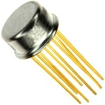
AD596/AD597 OUTLINE DIMENSIONS Dimensions shown in inches and (mm). 10-Pin Metal Can (TO-100) REFERENCE PLANE 8 9 0.750 (19.05) 2/ 0.185 (4.70) 0.500 (12.70) 0.160 (4.06) –5– 0.165 (4.19) 0.250 (6.35) MIN 0.110 (2.79) 1b 0.050 (1.27) MAX 3 8 C 6 7 5 0.370 (9.40)0.335 (8.51)0.335 (8.51)0.305 (7.75) (0B2.1.S91C25) 4 3 1089 00..004257 ((10..1649)) 2 1 0.034 (0.86) 0.019 (0.48) 0.230 (5.84) 0.027 (0.69) 0.016 (0.41) BSC 0.040 (1.02) MAX 36° BSC 0.021 (0.53) 0.045 (1.14) 0.016 (0.41) 0.010 (0.25) BASE & SEATING PLANE 8-Lead Small Outline (SOIC) (SO-8) 0.1968 (5.00) 0.1890 (4.80) 8 5 0.1574 (4.00) 0.2440 (6.20) 0.1497 (3.80) 1 4 0.2284 (5.80) PIN 1 0.0688 (1.75) 0.0196 (0.50) x 45° 0.0098 (0.25) 0.0532 (1.35) 0.0099 (0.25) 0.0040 (0.10) 8° SEPALTAINNGE 0(B.10.S52C070) 00..00119328 ((00..4395)) 00..00009785 ((00..2159)) 0° 00..00510600 ((10..2471)) A. S. U. N D I E T N RI P –8– REV. B