ICGOO在线商城 > 集成电路(IC) > PMIC - 监控器 > MAX6365PKA31+T

 Datasheet下载
- 型号: MAX6365PKA31+T
- 制造商: Maxim
- 库位|库存: xxxx|xxxx
- 要求:
| 数量阶梯 | 香港交货 | 国内含税 |
| +xxxx | $xxxx | ¥xxxx |
查看当月历史价格
查看今年历史价格
MAX6365PKA31+T产品简介:
ICGOO电子元器件商城为您提供MAX6365PKA31+T由Maxim设计生产,在icgoo商城现货销售,并且可以通过原厂、代理商等渠道进行代购。 MAX6365PKA31+T价格参考。MaximMAX6365PKA31+T封装/规格:PMIC - 监控器, 开路漏极或开路集电极 监控器 1 通道 SOT-23-8。您可以下载MAX6365PKA31+T参考资料、Datasheet数据手册功能说明书,资料中有MAX6365PKA31+T 详细功能的应用电路图电压和使用方法及教程。
Maxim Integrated的MAX6365PKA31+T是一款电源管理集成电路(PMIC),具体功能为电压监控器。该器件主要用于监测系统中的电源电压,确保其在安全范围内工作,广泛应用于需要高可靠性和稳定性的电子系统中。

其主要应用场景包括:

1. 工业控制系统:用于监测PLC、工控机等设备的供电电压,防止因电压异常导致系统崩溃或数据丢失。

2. 通信设备:在基站、路由器和交换机等通信设备中,监控电源状态,确保设备在电压波动时能够及时复位或告警。

3. 消费类电子产品:如高端音频设备、智能家电等,用于电源监控以提升系统稳定性与安全性。

4. 汽车电子系统:用于车载控制模块,监控车辆电源系统,防止因电压异常造成控制失灵。

5. 医疗设备:用于监测关键医疗仪器的电源状况,保障设备运行安全,避免因电源问题影响诊断或治疗。

该器件具备高精度电压检测、低功耗、宽工作温度范围等特性,适用于多种复杂环境,是保障系统稳定运行的重要组件。
| 参数 | 数值 |
| 产品目录 | 集成电路 (IC)半导体 |
| 描述 | IC SUPERVISOR MPU LP SOT23-8监控电路 uPower Supervisor |
| 产品分类 | |
| 品牌 | Maxim Integrated |
| 产品手册 | |
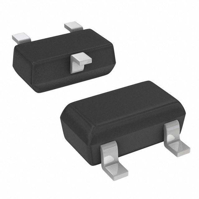
| 产品图片 |
|
| rohs | 符合RoHS无铅 / 符合限制有害物质指令(RoHS)规范要求 |
| 产品系列 | 电源管理 IC,监控电路,Maxim Integrated MAX6365PKA31+T- |
| NumberofInputsMonitored | 1 Input |
| 数据手册 | |
| 产品型号 | MAX6365PKA31+T |
| 产品培训模块 | http://www.digikey.cn/PTM/IndividualPTM.page?site=cn&lang=zhs&ptm=25703http://www.digikey.cn/PTM/IndividualPTM.page?site=cn&lang=zhs&ptm=25705 |
| 产品种类 | 监控电路 |
| 人工复位 | Manual Reset |
| 供应商器件封装 | SOT-23-8 |
| 其它名称 | MAX6365PKA31+T-ND |
| 功率失效检测 | No |
| 包装 | 带卷 (TR) |
| 受监控电压数 | 1 |
| 商标 | Maxim Integrated |
| 复位 | 低有效 |
| 复位超时 | 最小为 150 ms |
| 安装类型 | 表面贴装 |
| 安装风格 | SMD/SMT |
| 封装 | Reel |
| 封装/外壳 | SOT-23-8 |
| 封装/箱体 | SOT-23-8L |
| 工作温度 | -40°C ~ 85°C |
| 工作电源电流 | 15 uA |
| 工厂包装数量 | 2500 |
| 最大功率耗散 | 700 mW |
| 最大工作温度 | + 85 C |
| 最小工作温度 | - 40 C |
| 标准包装 | 2,500 |
| 欠电压阈值 | 3 V |
| 电压-阈值 | 3.08V |
| 电池备用开关 | Backup |
| 电源电压-最大 | 5.5 V |
| 电源电压-最小 | 0 V |
| 监视器 | No Watchdog |
| 类型 | Voltage Supervisory |
| 系列 | MAX6365P |
| 芯片启用信号 | Chip Enable |
| 被监测输入数 | 1 Input |
| 输出 | 开路漏极或开路集电极 |
| 输出类型 | Active Low, Open Drain |
| 过电压阈值 | 3.15 V |
| 重置延迟时间 | 280 ms |
| 阈值电压 | 2.5 V, 3 V, 3.3 V, 5 V |
| 零件号别名 | MAX6365P |


- 商务部:美国ITC正式对集成电路等产品启动337调查
- 曝三星4nm工艺存在良率问题 高通将骁龙8 Gen1或转产台积电
- 太阳诱电将投资9.5亿元在常州建新厂生产MLCC 预计2023年完工
- 英特尔发布欧洲新工厂建设计划 深化IDM 2.0 战略
- 台积电先进制程称霸业界 有大客户加持明年业绩稳了
- 达到5530亿美元!SIA预计今年全球半导体销售额将创下新高
- 英特尔拟将自动驾驶子公司Mobileye上市 估值或超500亿美元
- 三星加码芯片和SET,合并消费电子和移动部门,撤换高东真等 CEO
- 三星电子宣布重大人事变动 还合并消费电子和移动部门
- 海关总署:前11个月进口集成电路产品价值2.52万亿元 增长14.8%


PDF Datasheet 数据手册内容提取
19-1658; Rev 5; 10/11 SOT23, Low-Power µP Supervisory Circuits with Battery Backup and Chip-Enable Gating General Description Features M The MAX6365–MAX6368 supervisory circuits simplify (cid:1) Low +1.2V Operating Supply Voltage (VCCor VBATT) A power-supply monitoring, battery-backup control func- (cid:1) Precision Monitoring of +5.0V, +3.3V, +3.0V, and X tions, and memory write protection in microprocessor +2.5V Power-Supply Voltages (µP) systems. The circuits significantly improve the size, (cid:1) On-Board Gating of Chip-Enable Signals, 1.5ns 6 accuracy, and reliability of modern systems with an ultra- Propagation Delay 3 small integrated solution. (cid:1) Debounced Manual Reset Input (MAX6365) 6 (cid:1) Watchdog Timer, 1.6s Timeout (MAX6366) These devices perform four basic system functions: (cid:1) Battery-On Output Indicator (MAX6367) 5 1) Provide a µP reset output during VCC supply power- (cid:1) Auxiliary User-Adjustable RESET IN (MAX6368) – up, power-down, and brownout conditions. (cid:1) Low 10µA Quiescent Supply Current M 2) Internally control VCC to backup-battery switching to (cid:1) Three Available Output Structures A maintain data or low-power operation for CMOS Push-Pull RESET RAM, CMOS µPs, real-time clocks, and other digital Open-Drain RESET X logic when the main supply fails. Open-Drain RESET 6 (cid:1) RESET/RESET Valid Down to 1.2V Guaranteed 3) Provide memory write protection through internal 3 chip-enable gating during supply or processor faults. (VCCor VBATT) 6 (cid:1) Power-Supply Transient Immunity 4) Include one of the following options: a manual reset 8 (cid:1) 150ms min Reset Timeout Period input (MAX6365), a watchdog timer function (cid:1) Miniature 8-Pin SOT23 Package (MAX6366), a battery-on output (MAX6367), or an auxiliary user-adjustable reset input (MAX6368). Ordering Information The MAX6365–MAX6368 operate from VCC supply volt- PART* TEMP RANGE PIN-PACKAGE ages as low as 1.2V. The factory preset reset threshold voltages range from 2.32V to 4.63V (see the Ordering M A X6 3 6 5 LK A_ _-T -40°C to +85°C 8 SOT23 Information). In addition, each part is offered in three MAX6365PKA_ _-T -40°C to +85°C 8 SOT23 reset output versions: push-pull active low, open-drain MAX6365HKA_ _-T -40°C to +85°C 8 SOT23 active low, or open-drain active high (see the Selector M A X6 3 6 6 LK A_ _-T -40°C to +85°C 8 SOT23 Guide). The MAX6365–MAX6368 are available in minia- ture 8-pin SOT23 packages. M A X 6 36 6P K A_ _-T -40°C to +85°C 8 SOT23 M A X 6 36 6H K A_ _-T -40°C to +85°C 8 SOT23 Applications M A X6 3 6 7 LK A_ _-T -40°C to +85°C 8 SOT23 Critical µP/µC Power Portable/Battery- M A X 6 36 7P K A_ _-T -40°C to +85°C 8 SOT23 Monitoring Powered Equipment M A X 6 36 7P K A_ _/V-T -40°C to +85°C 8 SOT23 Fax Machines Set-Top Boxes M A X 6 36 7H K A_ _-T -40°C to +85°C 8 SOT23 Industrial Control POS Equipment M A X6 3 6 8 LK A_ _-T -40°C to +85°C 8 SOT23 Computers/Controllers M A X 6 36 8P K A_ _-T -40°C to +85°C 8 SOT23 Pin Configurations M A X 6 36 8H K A_ _-T -40°C to +85°C 8 SOT23 *These parts offer a choice of reset threshold voltages. From the TOP VIEW Reset Threshold Ranges table, insert the desired threshold volt- age code in the blank to complete the part number. SOT parts come in tape and reel only and must be ordered in 2500-piece RESET, RESET 1 8 CE OUT increments. See Device Marking Codes for a complete parts list, including SOT top marks and standard threshold versions. See CE IN 2 7 BATT Selector Guide for a listing of device features. MAX6365 GND 3 6 OUT Devices are available in both leaded and lead(Pb)-free packaging. Specify lead-free by replacing “-T” with “+T” when ordering. MR 4 5 VCC -Denotes a package containing lead(Pb). T= Tape and reel. /V Denotes an automotive qualified part. SOT23 Pin Configurations continued at end of data sheet. Typical Operating Circuit appears at end of data sheet. ________________________________________________________________Maxim Integrated Products 1 For pricing, delivery, and ordering information,please contact Maxim Directat 1-888-629-4642, or visit Maxim’s website at www.maxim-ic.com.
SOT23, Low-Power µP Supervisory Circuits with Battery Backup and Chip-Enable Gating 8 ABSOLUTE MAXIMUM RATINGS 6 Terminal Voltages (with respect to GND) Output Current 3 VCC, BATT, OUT.......................................................-0.3V to +6V OUT...............................Short-Circuit Protected for up to 10s 6 RESET(open drain), RESET (open drain)................-0.3V to +6V RESET, RESET, BATT ON, CEOUT...............................20mA BATT ON, RESET(push-pull), RESET IN, Continuous Power Dissipation (TA= +70°C) X WDI, CEIN, CEOUT...........................-0.3V to (VOUT+ 0.3V) 8-Pin SOT23 (derate 8.75mW/°C above +70°C)........700mW A MR..............................................................-0.3V to (VCC+ 0.3V) Operating Temperature Range...........................-40°C to +85°C Input Current Storage Temperature Range.............................-65°C to +150°C M VCCPeak..............................................................................1A Junction Temperature .....................................................+150°C VCCContinuous.............................................................250mA Lead Temperature (soldering, 10s).................................+300°C – BATT Peak.....................................................................250mA Soldering Temperature (reflow) 5 BATT Continuous.............................................................40mA Lead (Pb)-free packages..............................................+260°C 6 GND...............................................................................75mA Packages containing lead (Pb).....................................+240°C 3 Stresses beyond those listed under “Absolute Maximum Ratings” may cause permanent damage to the device. These are stress ratings only, and functional 6 operation of the device at these or any other conditions beyond those indicated in the operational sections of the specifications is not implied. Exposure to X absolute maximum rating conditions for extended periods may affect device reliability. A ELECTRICAL CHARACTERISTICS M (VCC = +2.4V to +5.5V, VBATT = +3.0V, CE IN = VCC, reset not asserted, TA = -40°C to +85°C. Typical values are at TA = +25°C, unless otherwise noted.) (Note 1) PARAMETER SYMBOL CONDITIONS MIN TYP MAX UNITS Operating Voltage Range VCC, VBATT No load 0 5.5 V (Note 2) VCC = 2.8V 10 30 Supply Current ICC No load, VCC > VTH VCC = 3.6V 12 35 µA (Excluding IOUT) VCC = 5.5V 15 50 Supply Current in Battery- IBACK VBATT = 2.8V, TA = +25°C 1 µA Backup Mode (Excluding IOUT) VCC = 0V TA = -40°C to +85°C 3 BATT Standby Current IBATT 5.5V > VCC > (VBATT TA = +25°C -0.10 +0.02 µA + 0.2V) TA = -40°C to +85°C -1.00 +0.05 VCC = 4.75V, IOUT = 150mA 3.1 VCC to OUT On-Resistance RON VCC = 3.15V, IOUT = 65mA 3.7 Ω VCC = 2.38V, IOUT = 25mA 4.6 VBATT = 4.5V, IOUT = 20mA VBATT - 0.2 Output Voltage in Battery- VOUT VBATT = 3.0V, IOUT = 10mA VBATT - V Backup Mode 0.15 VBATT = 2.25V, IOUT = 5mA VBATT - 0.15 Battery-Switchover Threshold Power-up 20 VSW VCC < VTH mV (VCC - VBATT) Power-down -20 MAX636_ _KA46 4.50 4.63 4.75 MAX636_ _KA44 4.25 4.38 4.50 MAX636_ _KA31 3.00 3.08 3.15 Reset Threshold VTH V MAX636_ _KA29 2.85 2.93 3.00 MAX636_ _KA26 2.55 2.63 2.70 MAX636_ _KA23 2.25 2.32 2.38 VCC Falling Reset Delay tRD VCC falling at 10V /ms 20 µs 2 _______________________________________________________________________________________
SOT23, Low-Power µP Supervisory Circuits with Battery Backup and Chip-Enable Gating ELECTRICAL CHARACTERISTICS (continued) M (VCC = +2.4V to +5.5V, VBATT = +3.0V, CE IN = VCC, reset not asserted, TA = -40°C to +85°C. Typical values are at TA = +25°C, A unless otherwise noted.) (Note 1) X PARAMETER SYMBOL CONDITIONS MIN TYP MAX UNITS 6 Reset Active Timeout Period tRP 150 280 ms 3 ISINK = 1.6mA, 0.3 6 Reset asserted, VCC > 2.1V 5 VOL VBATT = 0V ISINK = 100µA, – RESET Output Voltage 0.4 V VCC > 1.2V M VOH Reset not asserted ISOURCE = 500µA, 0.8 ✕ A (MAX636_L only) VCC > VTH(MAX) VCC X ISINK = 1.6mA, VOL Reset not asserted 0.3 6 VCC > VTH (MAX) 3 RESET Output Voltage Reset not asserted, ISOURCE = 1mA, 0.7 ✕ V 6 VOH VBATT = 0V VCC > 1.8V VCC 8 (MAX636_H only) ISOURCE = 200µA, 0.8 ✕ (Note 3) VCC > 1.2V VCC RES E T Outpu t Leakage Cu rr e nt ILKG MAX636_P and MAX636_H only 1 µA MANUAL RESET (MAX6365 only) 0.3 ✕ VIL VCC MR Input Voltage V 0.7 ✕ VIH VCC Pullup Resistance 20 kΩ Minimum Pulse Width 1 µs Glitch Immunity VCC = 3.3V 100 ns MR to Reset Delay VCC = 3.3V 120 ns WATCHDOG (MAX6366 only) Watchdog Timeout Period tWD 1.00 1.65 2.25 s Minimum WDI Input Pulse Width tWDI 100 ns 0.3 ✕ VIL VCC WDI Input Voltage V 0.7 ✕ VIH VCC WDI Input Current -1.0 1.0 µA BATT ON (MAX6367 only) Output Voltage VOL ISINK = 3.2mA, VBATT = 2.1V 0.4 V Sink current, VCC = 5V 60 mA Output Short-Circuit Current Source current, VBATT > 2V 10 30 100 µA _______________________________________________________________________________________ 3
SOT23, Low-Power µP Supervisory Circuits with Battery Backup and Chip-Enable Gating 8 ELECTRICAL CHARACTERISTICS (continued) 6 (VCC = +2.4V to +5.5V, VBATT = +3.0V, CE IN = VCC, reset not asserted, TA = -40°C to +85°C. Typical values are at TA = +25°C, 3 unless otherwise noted.) (Note 1) 6 PARAMETER SYMBOL CONDITIONS MIN TYP MAX UNITS X RESET IN (MAX6368 only) A RESET IN Threshold VRTH 1.185 1.235 1.285 V M RESET IN Leakage Current ±0.01 ±25 nA – RESET IN to Reset Delay VOD = 50mV, RESET IN falling 1.5 µs 5 CHIP-ENABLE GATING 6 CE IN Leakage Current Reset asserted ±1 µA 3 CE IN to CE OUT Resistance Reset not asserted (Note 4) 20 100 Ω 6 CE OUT Short-Circuit Current Reset asserted, VCE OUT = 0V 0.75 2.0 mA X CE IN to CE OUT Propagation 50Ω source, VCC = 4.75V 1.5 7 ns A Delay CLOAD = 6365 50pF VCC = 3.15V 2 9 M VCC = 5V, VCC > VBATT, ISOURCE = 100µA 0.8 ✕ VCC CE OUT Output Voltage High V VCC = 0V, VBATT > 2.2V, ISOURCE = 1µA VBATT - 0.1 Reset-to-CE OUT Delay 12 µs Note 1: All devices are 100% production tested at TA= +25°C. Limits over temperature are guaranteed by design. Note 2: VBATTcan be 0V anytime, or VCCcan go down to 0V if VBATTis active (except at startup). Note 3: RESET is pulled up to OUT. Specifications apply for OUT = VCCor OUT = BATT. Note 4: The chip-enable resistance is tested with VCC= VTH(MAX)and VCEIN= VCC/2. Typical Operating Characteristics (TA = +25°C, unless otherwise noted.) SUPPLY CURRENT BATTERY SUPPLY CURRENT BATT-TO-OUT ON-RESISTANCE vs. TEMPERATURE (NO LOAD) (BACKUP MODE) vs. TEMPERATURE vs. TEMPERATURE µUPPLY CURRENT (A) 111111215436 VVCBACT =T =5 .00VV MAX6365/8-01 µRY SUPPLY CURRENT (A) 00011.....64802 VBATT = 2.8V VBATT = 2.0V VCC = 0 MAX6365/8-02 ΩO-OUT ON-RESISTANCE () 437658 VVVBBBAAATTTTTT === 522...008VVV MAX6365/8-03 S 10 TTE T-T 2 A T B 0.2 BA 9 1 IOUT = 25mA VCC = 0V 8 0 0 -40 -20 0 20 40 60 80 -40 -20 0 20 40 60 80 -40 -20 0 20 40 60 80 TEMPERATURE (°C) TEMPERATURE (°C) TEMPERATURE (°C) 4 _______________________________________________________________________________________
SOT23, Low-Power µP Supervisory Circuits with Battery Backup and Chip-Enable Gating Typical Operating Characteristics (continued) M (TA = +25°C, unless otherwise noted.) A X VCC TO OUT ON-RESISTANCE RESET TIMEOUT PERIOD VCC TO RESET PROPAGATION DELAY 6 vs. TEMPERATURE vs. TEMPERATURE vs. TEMPERATURE 3 Ω TO OUT ON-RESISTANCE ()CC 000111......486204 VIOCUCT == V 22C.53CmV =A 4.5V VIOCUCT == 36.50mVA MAX6365/8-04 RESET TIMEOUT PERIOD (ms)122290015500 MAX6365/8-05 µPROPAGATION DELAY (s)1113764932005050505 VCC FALLING 01.2V5/mV/sms MAX6365/8-06 65–MAX6 V 0.2 IOUT = 150mA 15 10V/ms 3 6 0 190 0 -40 -20 0 20 40 60 80 -40 -20 0 20 40 60 80 -40 -20 0 20 40 60 80 8 TEMPERATURE (°C) TEMPERATURE (°C) TEMPERATURE (°C) RESET THRESHOLD MAXIMUM TRANSIENT DURATION BATTERY SUPPLY CURRENT vs. TEMPERATURE vs. RESET THRESHOLD OVERDRIVE vs. SUPPLY VOLTAGE 54..05 MAX636_ 46 (VTH = 4.63V) MAX6365/8-07 µN (s) 430500 MAX6365/8-08 µA) 1980 VTH = 2.93V MAX6365/8-09 THRESHOLD (V) 343...005 MAX636_ 26 (VTH = 2.63V) MUM TRANSIENT DURATIO 322110505000000 M(VATHX 6=3 46._RA6 EB34SVO6E)VTE OCCUCRUVRES TTERY SUPPLY CURRENT ( 35476 VVVBBBAAATTTTTT === 222...358VVV 2.5 AXI BA 2 M 50 MAX636_ 26 1 (VTH = 2.63V) 2.0 0 0 -40 -20 0 20 40 60 80 1 10 100 1000 10,000 0 0.5 1.0 1.5 2.0 2.5 3.0 3.5 TEMPERATURE (°C) RESET THRESHOLD OVERDRIVE VTH - VCC (mV) VCC (V) _______________________________________________________________________________________ 5
SOT23, Low-Power µP Supervisory Circuits with Battery Backup and Chip-Enable Gating 8 Typical Operating Characteristics (continued) 6 (TA = +25°C, unless otherwise noted.) 3 6 MAX6368 MAX6368 X RESET IN THRESHOLD RESET IN TO RESET PROPAGATION DELAY CHIP-ENABLE PROPAGATION DELAY A vs. TEMPERATURE vs. TEMPERATURE vs. CE OUT LOAD CAPACITANCE X6365–M V (V)RTH11..223356 MAX6365/8 -10 µPROPAGATION DELAY (s) 11222.....96852 VOD = 50mV MAX6365/8-11 PROPAGATION DELAY (ns) 3245 VDIMCRPEIV EINED R=A SN0OVC UET RO=C 5VE0CΩC VVCCCC == 53VV MAX6365/8-12 A 1 1.3 M 1.234 1.0 0 -40 -20 0 20 40 60 80 -40 -20 0 20 40 60 80 0 50 100 150 200 TEMPERATURE (°C) TEMPERATURE (°C) CLOAD (pF) MAX6366 CE IN TO CE OUT ON-RESISTANCE WATCHDOG TIMEOUT PERIOD vs. TEMPERATURE vs. TEMPERATURE ΩRESISTANCE () 122505 VCC = 3.0V MAX6365/8-13 UT PERIOD (s)11112.....98760 MAX6365/8-14 ON- MEO1.5 OUT 10 G TI1.4 O CE VCC = 5.0V CHDO1.3 CE IN T 5 VCE IN = VCC/2 WAT11..21 VCC = 5.0V VBATT = 0V VBATT = 0V 0 1.0 -40 -20 0 20 40 60 80 -40 -20 0 20 40 60 80 TEMPERATURE (°C) TEMPERATURE (°C) 6 _______________________________________________________________________________________
SOT23, Low-Power µP Supervisory Circuits with Battery Backup and Chip-Enable Gating Pin Description M PIN NAME FUNCTION A X Activ e-H i g h Reset Outpu t. RES E T assert s hig h contin uously wh en VC C is be lo w the re set thre shold (V T H) , MR is lo w, or RES E T IN is lo w. It assert s in pu ls es wh en the intern al wa tchdo g tim e s out. RES E T re ma in s 6 RESET assert ed for the re set tim e out pe ri o d (t RP) after VC C ri s es abo ve the re set thre shold , after the ma nual re set 3 in pu t go es fro m lo w to hig h , after RES E T IN go es hig h , or after the wa tchdo g tri g g e rs a re set event. 6 RES E T is an ope n-d r a in activ e-h ig h re set outpu t. 5 1 – Active-Low Reset Output. RESET asserts low continuously when V C C is below the reset threshold M (VTH), the manual reset input is low, or RESET IN is low. It asserts low in pulses when the internal watchdog times out. RESET remains asserted low for the reset timeout period (tRP) after V C C A RESET rises above the reset threshold, after the manual reset input goes from low to high, after RESET X IN goes high, or after the watchdog triggers a reset event. The MAX636_L is an active-low push- pull output, while the MAX636_P is an active-low open-drain output. 6 3 2 CE IN Chip-Enable Input. The input to chip-enable gating circuitry. Connect to GND or OUT if not used. 6 3 GND Ground 8 MAX6365 Manual-Reset Input. Maintaining logic low on MR asserts a reset. Reset output remains asserted as long as MR is low and for the reset timeout period (tRP) after MR transitions MR from low to high. Leave unconnected, or connect to VCC if not used. MR has an internal 20kΩ pullup to VCC. MAX6366 Watchdog Input. If WDI remains high or low for longer than the watchdog timeout period (t W D ), the internal watchdog timer runs out and a reset pulse is triggered for the reset WDI 4 timeout period (tRP). The internal watchdog clears whenever reset asserts or whenever WDI sees a rising or falling edge (Figure 2). BATT ON MAX6367 Battery-On Output. BATT ON goes high when in battery-backup mode. MAX6368 Reset Input. When RESET IN falls below 1.235V, reset asserts. Reset output remains RESET IN asserted as long as RESET IN is low and for at least tRP after RESET IN goes high. Supply Voltage, 1.2V to 5.5V. Reset asserts when V C C drops below the reset threshold voltage 5 VCC (VTH). Reset remains asserted until V C C rises above VTH and for at least tRP after V C C rises above VTH. Output. OUT sources from V C C when not in reset and from the greater of VCC or BATT when V C C 6 OUT is below the reset threshold. Backup-Battery Input. When V C C falls below the reset threshold, OUT switches to BATT if VBATT 7 BATT is 20mV greater than V C C . When V C C rises 20mV above VBATT, OUT switches to V C C . The 40mV hysteresis prevents repeated switching if VCC falls slowly. Chip-Enable Output. CE OUT goes low only when CE IN is low and reset is not asserted. If CE IN is low when reset is asserted, CE OUT will stay low for 12µs (typ) or until CE IN goes high, 8 CE OUT whichever occurs first. _______________________________________________________________________________________ 7
SOT23, Low-Power µP Supervisory Circuits with Battery Backup and Chip-Enable Gating 8 Functional Diagram 6 3 6 BATT ON (MAX6367 ONLY) X A 1.235V M MAX6365 MAX6366 – VCC MAX6367 5 MAX6368 6 OUT 3 CHIP-ENABLE OUTPUT 6 CONTROL X A BATT M CE IN CE OUT 20k RESET MR GENERATOR RESET (MAX6365 ONLY) (RESET) WDI WATCHDOG WATCHDOG (MAX6366 ONLY) TRANSITION TIMER DETECTOR RESET IN (MAX6368 ONLY) 1.235V GND Detailed Description CMOS RAM in the event of a power failure. During nor- mal operation, the CE gate is enabled and passes all The Typical Operating Circuitshows a typical connec- CE transitions. When reset asserts, this path becomes tion for the MAX6365–MAX6368. OUT powers the static disabled, preventing erroneous data from corrupting random-access memory (SRAM). If VCC is greater than the CMOS RAM. All of these devices use a series trans- the reset threshold (VTH), or if VCC is lower than VTH mission gate from CE IN to CE OUT. The 2ns propaga- but higher than VBATT, VCC is connected to OUT. If tion delay from CE IN to CE OUT allows the devices to VCC is lower than VTH and VCC is less than VBATT, be used with most µPs and high-speed DSPs. BATT is connected to OUT. OUT supplies up to 150mA from VCC. In battery-backup mode, an internal MOSFET During normal operation, CE IN is connected to CE connects the backup battery to OUT. The on-resistance OUT through a low on-resistance transmission gate. of the MOSFET is a function of backup-battery voltage This is valid when reset is not asserted. If CE IN is high and is shown in the BATT-to-OUT On-Resistance vs. when reset is asserted, CE OUT remains high regard- Temperature graph in the Typical Operating Char- less of any subsequent transitions on CE IN during the acteristics. reset event. If CE IN is low when reset is asserted, CE OUT is held Chip-Enable Signal Gating low for 12µs to allow completion of the read/write oper- The MAX6365–MAX6368 provide internal gating of CE ation (Figure 1). After the 12µs delay expires, the CE signals to prevent erroneous data from being written to 8 _______________________________________________________________________________________
SOT23, Low-Power µP Supervisory Circuits with Battery Backup and Chip-Enable Gating OUT goes high and stays high regardless of any sub- Table 1. Input and Output Status in M sequent transitions on CE IN during the reset event. Battery-Backup Mode A When CE OUT is disconnected from CE IN, CE OUT is actively pulled up to OUT. PIN STATUS X The propagation delay through the chip-enable circuit- VCC Disconnected from OUT 6 ry depends on both the source impedance of the drive OUT Connected to BATT 3 to CE IN and the capacitive loading at CE OUT. The 6 chip-enable propagation delay is production tested Connected to OUT. Current drawn from from the 50% point of CE IN to the 50% point of CE BATT the battery is less than 1µA (at VBATT = 5 OUT, using a 50Ω driver and 50pF load capacitance. 2.8V, excluding IOUT) when VCC = 0V. – M Minimize the capacitive load at CE OUT to minimize RESET/RESET Asserted propagation delay, and use a low-output-impedance BATT ON High state A driver. MR, RESET IN, X Backup-Battery Switchover Inputs ignored CE IN, WDI 6 In a brownout or power failure, it may be necessary to CE OUT Connected to OUT 3 preserve the contents of the RAM. With a backup bat- tery installed at BATT, the MAX6365–MAX6368 auto- 6 matically switch the RAM to backup power when VCC Manual Reset Input (MAX6365 Only) 8 falls. The MAX6367 has a BATT ON output that goes Many µP-based products require manual reset capabili- high in battery-backup mode. These devices require ty, allowing the user or external logic circuitry to initiate a two conditions before switching to battery-backup reset. For the MAX6365, a logic low on MRasserts reset. mode: Reset remains asserted while MR is low and for a mini- 1) VCCmust be below the reset threshold. mum of 150ms (tRP) after it returns high. MRhas an inter- nal 20kΩpullup resistor to VCC. This input can be driven 2) VCCmust be below VBATT. with TTL/CMOS logic levels or with open-drain/collector Table 1 lists the status of the inputs and outputs in bat- outputs. Connect a normally open momentary switch tery-backup mode. The devices do not power up if the from MRto GND to create a manual reset function; exter- only voltage source is on BATT. OUT only powers up nal debounce circuitry is not required. If MR is driven from VCCat startup. from long cables or the device is used in a noisy environ- ment, connect a 0.1µF capacitor from MRto GND to pro- vide additional noise immunity. VCC OR BATT RESET THRESHOLD VTH CE IN CE OUT RESET-TO-CE OUT DELAY (12µs) * tRD tRD RESET tRP tRP RESET *IF CE IN GOES HIGH BEFORE RESET ASSERTS, CE OUT GOES HIGH WITHOUT DELAY AS CE IN GOES HIGH. Figure 1. Reset and Chip-Enable Timing _______________________________________________________________________________________ 9
SOT23, Low-Power µP Supervisory Circuits with Battery Backup and Chip-Enable Gating 8 6 WDI 3 6 X tRP tRP tWD tWD A RESET M – 5 tWD = WATCHDOG TIMEOUT PERIOD 6 tRP = RESET TIMEOUT PERIOD 3 Figure 2. MAX6366 Watchdog Timeout Period and Reset Active Time 6 X A Watchdog Input (MAX6366 Only) where VREF = 1.235V. To simplify the resistor selection, The watchdog monitors µP activity through the watch- choose a value for R2 and calculate R1: M dog input (WDI). If the µP becomes inactive, reset R1 = R2 [(VRTH / VREF) - 1] asserts. To use the watchdog function, connect WDI to Since the input current at RESET IN is 25nA (max), a bus line or µP I/O line. A change of state (high to low, large values (up to 1MΩ) can be used for R2 with no low to high, or a minimum 100ns pulse) resets the significant loss in accuracy. For example, in the Typical watchdog timer. If WDI remains high or low for longer Operating Circuit, the MAX6368 monitors two supply than the watchdog timeout period (tWD), the internal voltages. To monitor the secondary 5V logic or analog watchdog timer runs out and a reset pulse is triggered supply with a 4.60V nominal programmed reset thresh- for the reset timeout period (tRP). The internal watchdog old, choose R2 = 100kΩ, and calculate R1 = 273kΩ. timer clears whenever reset asserts or whenever WDI sees a rising or falling edge. If WDI remains in either a Reset Output high or low state, a reset pulse asserts periodically after A µP’s reset input starts the µP in a known state. The every tWD(Figure 2). MAX6365–MAX6368 µP supervisory circuits assert a reset to prevent code-execution errors during power- BATT ON Indicator (MAX6367 Only) up, power-down, and brownout conditions. RESET is BATT ON is a push-pull output that drives high when in guaranteed to be a logic low or logic high, depending battery-backup mode. BATT ON typically sinks 3.2mA on the device chosen (see the Ordering Information). at 0.1V saturation voltage. In battery-backup mode, this terminal sources approximately 10µA from OUT. Use RESET or RESET asserts when VCC is below the reset BATT ON to indicate battery-switchover status or to threshold and for at least 150ms (tRP) after VCC rises above the reset threshold. RESET or RESET also supply base drive to an external pass transistor for asserts when MRis low (MAX6365) and when RESET IN higher current applications (Figure 3). is less than 1.235V (MAX6368). The MAX6366 watch- RESET IN Comparator (MAX6368 Only) dog function will cause RESET (or RESET) to assert in RESET IN is compared to an internal 1.235V reference. pulses following a watchdog timeout (Figure 2). If the voltage at RESET IN is less than 1.235V, reset Applications Information asserts. Use the RESET IN comparator as an undervolt- age detector to signal a failing power supply or as a Operation Without secondary power-supply reset monitor. a Backup Power Source To program the reset threshold (VRTH) of the secondary The MAX6365–MAX6368 provide battery-backup func- power supply, use the following (see Typical Operating tions. If a backup power source is not used, connect Circuit): BATT to GND and OUT to VCC. VRTH= VREF(R1 / R2 + 1) 10 ______________________________________________________________________________________
SOT23, Low-Power µP Supervisory Circuits with Battery Backup and Chip-Enable Gating Watchdog Software Considerations when VCCexperiences only small glitches is usually not M One way to help the watchdog timer monitor the soft- desirable. ware execution more closely is to set and reset the A The Typical Operating Characteristicssection has a watchdog at different points in the program rather than Maximum Transient Duration vs. Reset Threshold X pulsing the watchdog input periodically. Figure 4 Overdrive graph for which reset is not asserted. The 6 shows a flow diagram in which the I/O driving the graph was produced using negative-going VCCpulses, 3 watchdog is set low in the beginning of the program, starting at VCCand ending below the reset threshold by set high at the beginning of every subroutine or loop, 6 the magnitude indicated (reset threshold overdrive). and set low again when the program returns to the The graph shows the maximum pulse width that a neg- 5 beginning. If the program should hang in any subrou- ative-going VCC transient can typically have without – tine, the problem would be quickly corrected. triggering a reset pulse. As the amplitude of the tran- M sient increases (i.e., goes further below the reset Replacing the Backup Battery A threshold), the maximum allowable pulse width When VCCis above VTH, the backup power source can be removed without danger of triggering a reset pulse. decreases. Typically, a VCC transient that goes 100mV X below the reset threshold and lasts for 30µs will not trig- The device does not enter battery-backup mode when 6 ger a reset pulse. VCCstays above the reset threshold voltage. 3 A 0.1µF bypass capacitor mounted close to the VCC 6 Negative-Going VCCTransients pin provides additional transient immunity. These supervisors are relatively immune to short-dura- 8 tion, negative-going VCC transients. Resetting the µP +2.4V TO +5.5V START 0.1µF VCC BATT ON SET WDI OUT LOW BATT CE OUT CE MAX6367 CMOS RAM SUBROUTINE OR PROGRAM LOOP ADDRESS CE IN SET WDI DECODE HIGH A0–A15 µP GND RESET RESET RETURN Figure 3. MAX6367 BATT ON Driving an External Pass Transistor END Figure 4. Watchdog Flow Diagram ______________________________________________________________________________________ 11
SOT23, Low-Power µP Supervisory Circuits with Battery Backup and Chip-Enable Gating 8 Reset Threshold Ranges 6 RESET THRESHOLD RANGES (V) 3 SUFFIX MIN TYP MAX 6 46 4.50 4.63 4.75 X 44 4.25 4.38 4.50 A 31 3.00 3.08 3.15 M 29 2.85 2.93 3.00 26 2.55 2.63 2.70 – 23 2.25 2.32 2.38 5 6 3 Device Marking Codes 6 X PART TOP MARK PART TOP MARK PART TOP MARK A MAX6365LKA23 AAAM MAX6366PKA23 AABK MAX6367HKA23 AACI M MAX6365LKA26 AAAL MAX6366PKA26 AABJ MAX6367HKA26 AACH MAX6365LKA29* AAAK MAX6366PKA29* AABI MAX6367HKA29 AACG MAX6365LKA31 AAAJ MAX6366PKA31 AABH MAX6367HKA31 AACF MAX6365LKA44 AAAI MAX6366PKA44 AABG MAX6367HKA44 AACE MAX6365LKA46* AAAH MAX6366PKA46* AABF MAX6367HKA46* AACD MAX6365PKA23 AAAS MAX6366HKA23 AABQ MAX6368LKA23 AACO MAX6365PKA26 AAAR MAX6366HKA26 AABP MAX6368LKA26 AACN MAX6365PKA29* AAAQ MAX6366HKA29 AABO MAX6368LKA29* AACM MAX6365PKA31 AAAP MAX6366HKA31 AABN MAX6368LKA31 AACL MAX6365PKA44 AAAO MAX6366HKA44 AABM MAX6368LKA44 AACK MAX6365PKA46* AAAN MAX6366HKA46* AABL MAX6368LKA46* AACJ MAX6365HKA23 AAAY MAX6367LKA23 AABW MAX6368PKA23 AACU MAX6365HKA26 AAAX MAX6367LKA26 AABV MAX6368PKA26 AACT MAX6365HKA29 AAAW MAX6367LKA29* AABU MAX6368PKA29* AACS MAX6365HKA31 AAAV MAX6367LKA31 AABT MAX6368PKA31 AACR MAX6365HKA44 AAAU MAX6367LKA44 AABS MAX6368PKA44 AACQ MAX6365HKA46* AAAT MAX6367LKA46* AABR MAX6368PKA46* AACP MAX6366LKA23 AABE MAX6367PKA23 AACC MAX6368HKA23 AADA MAX6366LKA26 AABD MAX6367PKA26 AACB MAX6368HKA26 AACZ MAX6366LKA29* AABC MAX6367PKA29* AACA MAX6368HKA29 AACY MAX6366LKA31 AABB MAX6367PKA31 AABZ MAX6368HKA31 AACX MAX6366LKA44 AABA MAX6367PKA44 AABY MAX6368HKA44 AACW MAX6366LKA46* AAAZ MAX6367PKA46* AABX MAX6368HKA46* AACV *These standard versions are available in small quantities through Maxim Distribution. Sample stock is generally held on standard versions only. Contact factory for availability of nonstandard versions. 12 ______________________________________________________________________________________
SOT23, Low-Power µP Supervisory Circuits with Battery Backup and Chip-Enable Gating Selector Guide M A MANUAL WATCH- BATT RESET RESET RESET RESET CHIP- X PART RESET DOG ON IN PUSH- OPEN- OPEN- ENABLE INPUT INPUT PULL DRAIN DRAIN GATING 6 MAX6365LKA__ (cid:1) (cid:1) (cid:1) 3 MAX6365PKA__ (cid:1) (cid:1) (cid:1) 6 5 MAX6365HKA__ (cid:1) (cid:1) (cid:1) – MAX6366LKA__ (cid:1) (cid:1) (cid:1) M MAX6366PKA__ (cid:1) (cid:1) (cid:1) MAX6366HKA__ (cid:1) (cid:1) (cid:1) A MAX6367LKA__ (cid:1) (cid:1) (cid:1) X MAX6367PKA__ (cid:1) (cid:1) (cid:1) 6 MAX6367HKA__ (cid:1) (cid:1) (cid:1) 3 MAX6368LKA__ (cid:1) (cid:1) (cid:1) 6 MAX6368PKA__ (cid:1) (cid:1) (cid:1) 8 MAX6368HKA__ (cid:1) (cid:1) (cid:1) Pin Configurations (continued) TOP VIEW RESET, RESET 1 8 CE OUT RESET, RESET 1 8 CE OUT CE IN 2 7 BATT CE IN 2 7 BATT MAX6366 MAX6367 GND 3 6 OUT GND 3 6 OUT WDI 4 5 VCC BATT ON 4 5 VCC SOT23 SOT23 RESET, RESET 1 8 CE OUT CE IN 2 7 BATT MAX6368 GND 3 6 OUT RESET IN 4 5 VCC SOT23 ______________________________________________________________________________________ 13
SOT23, Low-Power µP Supervisory Circuits with Battery Backup and Chip-Enable Gating 8 Typical Operating Circuit 6 3 6 X +2.4V TO +5.5V A CMOS REAL- M 0.1µF RAM TIME CE CLOCK – 5 VCC BATT OUT 6 3 MAX6366 0.1µF 6 SECONDARY MAX6368 A0–A15 DC VOLTAGE X RESET RESET R1 A µP M RESET IN* WDI** I/O CE IN CE OUT R2 ADDRESS GND DECODE *RESET IN APPLIES TO MAX6368 ONLY. **WDI APPLIES TO MAX6366 ONLY. Chip Information Package Information PROCESS: CMOS For the latest package outline information and land patterns (footprints), go to www.maxim-ic.com/packages. Note that a “+”, “#”, or “-” in the package code indicates RoHS status only. Package drawings may show a different suffix character, but the drawing pertains to the package regardless of RoHS status. PACKAGE PACKAGE OUTLINE LAND TYPE CODE NO. PATTERN NO. 8 SOT23 K8SN-1 21-0078 90-0176 14 ______________________________________________________________________________________
SOT23, Low-Power µP Supervisory Circuits with Battery Backup and Chip-Enable Gating Revision History M A REVISION REVISION DESCRIPTION PAGES X NUMBER DATE CHANGED 6 4 5/09 Added automotive part number to Ordering Information table 1 3 5 10/11 Updated the Electrical Characteristics. 2 6 5 – M A X 6 3 6 8 Maxim cannot assume responsibility for use of any circuitry other than circuitry entirely embodied in a Maxim product. No circuit patent licenses are implied. Maxim reserves the right to change the circuitry and specifications without notice at any time. The parametric values (min and max limits) shown in the Electrical Characteristics table are guaranteed. Other parametric values quoted in this data sheet are provided for guidance. 15 ____________________Maxim Integrated Products, 120 San Gabriel Drive, Sunnyvale, CA 94086 408-737-7600 © 2011 Maxim Integrated Products Maxim is a registered trademark of Maxim Integrated Products, Inc.
Mouser Electronics Authorized Distributor Click to View Pricing, Inventory, Delivery & Lifecycle Information: M axim Integrated: MAX6368HKA31+T MAX6366PKA31+T MAX6367PKA29+T MAX6365HKA23+T MAX6365HKA29+T MAX6365HKA31+T MAX6365HKA44+T MAX6365HKA46+T MAX6365LKA23+T MAX6365LKA26+T MAX6365LKA29+T MAX6365LKA31+T MAX6365LKA44+T MAX6365LKA46+T MAX6365PKA23+T MAX6365PKA26+T MAX6365PKA29+T MAX6365PKA31+T MAX6365PKA44+T MAX6365PKA46+T MAX6366HKA23+T MAX6366HKA26+T MAX6366HKA29+T MAX6366HKA31+T MAX6366HKA44+T MAX6366HKA46+T MAX6366LKA23+T MAX6366LKA26+T MAX6366LKA29+T MAX6366LKA31+T MAX6366LKA44+T MAX6366LKA46+T MAX6366PKA23+T MAX6366PKA26+T MAX6366PKA29+T MAX6366PKA44+T MAX6366PKA46+T MAX6367HKA29+T MAX6367HKA31+T MAX6367HKA46+T MAX6367LKA26+T MAX6367LKA29+T MAX6367LKA31+T MAX6367LKA46+T MAX6367PKA23+T MAX6367PKA26+T MAX6367PKA31+T MAX6367PKA31/V+T MAX6367PKA44+T MAX6367PKA46+T MAX6368HKA23+T MAX6368HKA26+T MAX6368HKA46+T MAX6368LKA23+T MAX6368LKA26+T MAX6368LKA29+T MAX6368LKA31+T MAX6368LKA44+T MAX6368LKA46+T MAX6368PKA23+T MAX6368PKA26+T MAX6368PKA29+T MAX6368PKA31+T MAX6368PKA44+T MAX6368PKA46+T