ICGOO在线商城 > 集成电路(IC) > PMIC - 以太网供电(PoE) 控制器 > MAX5982CETE+T

 Datasheet下载
- 型号: MAX5982CETE+T
- 制造商: Maxim
- 库位|库存: xxxx|xxxx
- 要求:
| 数量阶梯 | 香港交货 | 国内含税 |
| +xxxx | $xxxx | ¥xxxx |
查看当月历史价格
查看今年历史价格
MAX5982CETE+T产品简介:
ICGOO电子元器件商城为您提供MAX5982CETE+T由Maxim设计生产,在icgoo商城现货销售,并且可以通过原厂、代理商等渠道进行代购。 MAX5982CETE+T价格参考。MaximMAX5982CETE+T封装/规格:PMIC - 以太网供电(PoE) 控制器, Power Over Ethernet Controller 1 Channel 802.3at (PoE+), 802.3af (PoE) 16-TQFN (5x5)。您可以下载MAX5982CETE+T参考资料、Datasheet数据手册功能说明书,资料中有MAX5982CETE+T 详细功能的应用电路图电压和使用方法及教程。
MAX5982CETE+T 是 Maxim Integrated 公司推出的一款 PMIC(电源管理集成电路)以太网供电(PoE)控制器。该器件主要用于支持 IEEE 802.3af/at 标准的 PoE 系统,为需要通过以太网电缆传输电力和数据的设备提供高效的电源管理解决方案。

 应用场景:

1. 网络摄像头(IP 摄像头):
   - MAX5982CETE+T 可以为 IP 摄像头提供稳定的电源供应,支持高分辨率视频录制和传输。
   - 在安防监控领域,IP 摄像头通常部署在难以布线的地方,PoE 技术简化了安装过程,仅需一根以太网电缆即可同时传输数据和电力。

2. 无线接入点(Wi-Fi 路由器/接入点):
   - 该芯片适用于无线接入点或路由器,为其提供可靠的电源管理。
   - 通过 PoE 技术,无线接入点可以灵活地安装在天花板、墙壁或其他不便布电的位置,同时保持稳定的数据和电力传输。

3. VoIP 电话:
   - VoIP 电话需要同时进行语音通信和电力供应,MAX5982CETE+T 可以确保设备在断电情况下仍能正常运行。
   - 支持 IEEE 802.3af/at 标准,能够满足不同功率需求的 VoIP 设备。

4. 楼宇自动化系统:
   - 在智能建筑中,MAX5982CETE+T 可用于控制传感器、执行器和其他联网设备。
   - 这些设备通常分布在建筑物的各个角落,PoE 技术减少了对额外电源插座的需求,降低了安装成本。

5. 工业物联网(IIoT)设备:
   - 工业环境中,传感器、控制器和其他智能设备需要可靠且低维护的电源解决方案。
   - MAX5982CETE+T 提供高效、稳定的电源管理功能,适合恶劣环境下的长时间运行。

6. 零售终端设备(如 POS 机):
   - 在零售行业中,PoE 技术可用于连接收银机、条码扫描仪等设备。
   - MAX5982CETE+T 的高集成度和灵活性使得这些设备的部署更加便捷。

7. 智能家居设备:
   - 包括智能门锁、温控器和照明控制系统在内的智能家居设备,可以通过 PoE 技术实现远程管理和控制。
   - 该芯片支持多种功率等级,适应不同的智能家居应用场景。

 总结:
MAX5982CETE+T 的主要优势在于其对 IEEE 802.3af/at 标准的支持以及高效率的电源管理能力,适用于需要通过以太网供电的各类设备。无论是商业、工业还是家庭环境,该芯片都能提供稳定、灵活的电源解决方案,简化系统设计并降低部署成本。
| 参数 | 数值 |
| 产品目录 | 集成电路 (IC) |
| 描述 | IC CTRLR PD IEEE 802.3AF 16TQFN |
| 产品分类 | PMIC - 以太网供电 (PoE) 控制器 |
| 品牌 | Maxim Integrated |
| 数据手册 | |
| 产品图片 | |
| 产品型号 | MAX5982CETE+T |
| rohs | 无铅 / 符合限制有害物质指令(RoHS)规范要求 |
| 产品系列 | - |
| 产品培训模块 | http://www.digikey.cn/PTM/IndividualPTM.page?site=cn&lang=zhs&ptm=25703http://www.digikey.cn/PTM/IndividualPTM.page?site=cn&lang=zhs&ptm=25705 |
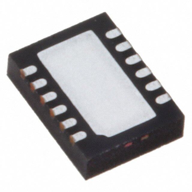
| 供应商器件封装 | 16-TQFN (5x5) |
| 其它名称 | MAX5982CETE+TCT |
| 内部开关 | 是 |
| 功率-最大值 | 70W |
| 包装 | 剪切带 (CT) |
| 封装/外壳 | 16-WQFN 裸露焊盘 |
| 工作温度 | -40°C ~ 85°C |
| 标准 | 802.3at (PoE+), 802.3af (PoE) |
| 标准包装 | 1 |
| 特色产品 | http://www.digikey.cn/product-highlights/cn/zh/maxim-max5982-mosfet/2480 |
| 电压-电源 | 36.6 V ~ 60 V |
| 电流-电源 | 250µA |
| 类型 | 控制器 (PD) |
| 辅助作用 | 是 |
| 通道数 | 1 |


- 商务部:美国ITC正式对集成电路等产品启动337调查
- 曝三星4nm工艺存在良率问题 高通将骁龙8 Gen1或转产台积电
- 太阳诱电将投资9.5亿元在常州建新厂生产MLCC 预计2023年完工
- 英特尔发布欧洲新工厂建设计划 深化IDM 2.0 战略
- 台积电先进制程称霸业界 有大客户加持明年业绩稳了
- 达到5530亿美元!SIA预计今年全球半导体销售额将创下新高
- 英特尔拟将自动驾驶子公司Mobileye上市 估值或超500亿美元
- 三星加码芯片和SET,合并消费电子和移动部门,撤换高东真等 CEO
- 三星电子宣布重大人事变动 还合并消费电子和移动部门
- 海关总署:前11个月进口集成电路产品价值2.52万亿元 增长14.8%


PDF Datasheet 数据手册内容提取
EVALUATION KIT AVAILABLE Click here for production status of specific part numbers. MAX5982A/MAX5982B/ IEEE 802.3af/at-Compliant, MAX5982C Powered Device Interface Controllers with Integrated 70W High-Power MOSFET General Description Features The MAX5982A/MAX5982B/MAX5982C provide a com- ● Sleep Mode and Ultra-Low-Power Sleep plete interface for a powered device (PD) to comply with (MAX5982A/MAX5982B) the IEEE® 802.3af/at standard in a power-over-Ethernet ● IEEE 802.3af/at Compliant (PoE) system. The MAX5982A/MAX5982B/MAX5982C ● 2-Event Classification or an External Wall Adapter provide the PD with a detection signature, classifica- Indicator Output tion signature, and an integrated isolation power switch with inrush current control. During the inrush period, the ● Simplified Wall Adapter Interface MAX5982A/MAX5982B/MAX5982C limit the current to ● PoE Classification 0–5 less than 182mA before switching to the higher current ● 100V Input Absolute Maximum Rating limit (1700mA to 2100mA) when the isolation power MOSFET is fully enhanced. The devices feature an input ● Inrush Current Limit of 182mA Maximum UVLO with wide hysteresis and long deglitch time to com- ● Current Limit During Normal Operation Between pensate for twisted-pair cable resistive drop and to assure 1700mA and 2100mA glitch-free transition during power-on/-off conditions. The ● Current Limit and Foldback MAX5982A/MAX5982B/MAX5982C can withstand up to 100V at the input. ● Legacy UVLO at 36V The MAX5982A/MAX5982B/MAX5982C support a ● LED Driver with Programmable LED Current 2-Event classification method as specified in the IEEE (MAX5982A/MAX5982B) 802.3at standard and provide a signal to indicate when ● Overtemperature Protection probed by a Type 2 power sourcing equipment (PSE). ● Thermally Enhanced, 5mm x 5mm, 16-Pin TQFN The devices detect the presence of a wall adapter power source connection and allow a smooth switchover from Applications the PoE power source to the wall power adapter. ● IEEE 802.3af/at Powered Devices The MAX5982A/MAX5982B/MAX5982C also provide a ● IP Phones, Wireless Access Nodes, IP Security power-good (PG) signal, two-step current limit and fold- Cameras back, overtemperature protection, and di/dt limit. A sleep ● WiMAX™ Base Stations mode feature in the MAX5982A/MAX5982B provides low power consumption while supporting Maintain Power Signature (MPS). An ultra-low-power sleep mode feature in the MAX5982A/MAX5982B further reduces power consumption while still supporting MPS. The MAX5982A/ MAX5982B also feature an LED driver that is automati- Ordering Information appears at end of data sheet. cally activated during sleep mode. The MAX5982A/MAX5982B/MAX5982C are available in a 16-pin, 5mm x 5mm, TQFN power package. These devices are rated over the -40°C to +125°C extended temperature range. WiMAX is a trademark of WiMAX Forum. IEEE is a registered service mark of the Institute of Electrical and Electronics Engineers, Inc. 19-5960; Rev 1; 3/19
MAX5982A/MAX5982B/ IEEE 802.3af/at-Compliant, MAX5982C Powered Device Interface Controllers with Integrated 70W High-Power MOSFET Absolute Maximum Ratings VDD to VSS ..........................................................-0.3V to +100V Operating Temperature Range .........................-40°C to +125°C DET, RTN, WAD, PG, 2EC to VSS ......................-0.3V to +100V Maximum Junction Temperature .....................................+150°C CLS, SL, WK, ULP, LED to VSS .............................-0.3V to +6V Storage Temperature Range ............................-65°C to +150°C Maximum Current on CLS (100ms maximum) .................100mA Lead Temperature (soldering, 10s) .................................+300°C Continuous Power Dissipation (TA = +70°C) (Note 1) Soldering Temperature (reflow) .......................................+260°C TQFN (derate 28.6mW/°C above +70°C) Multilayer Board ......................................................2285.7mW Stresses beyond those listed under “Absolute Maximum Ratings” may cause permanent damage to the device. These are stress ratings only, and functional operation of the device at these or any other conditions beyond those indicated in the operational sections of the specifications is not implied. Exposure to absolute maximum rating conditions for extended periods may affect device reliability. Note 1: Maximum power dissipation is obtained using JEDEC JESD51-5 and JESD51-7 specifications. Package Thermal Characteristics (Note 2) TQFN Junction-to-Ambient Thermal Resistance (θJA) ..........35°C/W Junction-to-Case Thermal Resistance (θJC) ..............2.7°C/W Note 2: Package thermal resistances were obtained using the method described in JEDEC specification JESD51-7, using a four-layer board. For detailed information on package thermal considerations, refer to www.maximintegrated.com/thermal-tutorial. Electrical Characteristics (VIN = (VDD - VSS) = 48V, RDET = 24.9kΩ, RCLS = 615Ω, and RSL = 60.4kΩ. RTN, WAD, PG, 2EC, WK, and ULP unconnected, all voltages are referenced to VSS, unless otherwise noted. TA = TJ = -40°C to +125°C, unless otherwise noted. Typical values are at TA = +25°C.) (Note 3) PARAMETER SYMBOL CONDITIONS MIN TYP MAX UNITS DETECTION MODE Input Offset Current IOFFSET VIN = 1.4V to 10.1V (Note 4) 10 µA Effective Differential Input dR VIN = 1.4V up to 10.1V with 1V step, 23.95 25.00 25.50 kΩ Resistance VDD = RTN = WAD = PG = 2EC (Note 5) CLASSIFICATION MODE Classification Disable Threshold VTH,CLS VIN rising (Note 6) 22.0 22.8 23.6 V Classification Stability Time 0.2 ms Class 0, RCLS = 615Ω 0 3.96 VIN = 12.5V to Class 1, RCLS = 117Ω 9.12 11.88 Classification Current ICLASS R20T.N5V =, VWDADD = = CCllaassss 32,, RRCCLLSS == 6463..57ΩΩ 1276..23 1299..87 mA PG = 2EC Class 4, RCLS = 30.9Ω 36.4 43.6 Class 5, RCLS = 21.3Ω 52.7 63.3 TYPE 2 (802.3at) CLASSIFICATION MODE Mark Event Threshold VTHM VIN falling 10.1 10.7 11.6 V Hysteresis on Mark Event 0.82 V Threshold Mark Event Current IMARK VVIINN f≤a 1lli0n.g1 Vto enter mark event, 5.2V ≤ 0.25 0.85 mA Reset Event Threshold VTHR VIN falling 2.7 3.8 5.2 V www.maximintegrated.com Maxim Integrated │ 2
MAX5982A/MAX5982B/ IEEE 802.3af/at-Compliant, MAX5982C Powered Device Interface Controllers with Integrated 70W High-Power MOSFET Electrical Characteristics (continued) (VIN = (VDD - VSS) = 48V, RDET = 24.9kΩ, RCLS = 615Ω, and RSL = 60.4kΩ. RTN, WAD, PG, 2EC, WK, and ULP unconnected, all voltages are referenced to VSS, unless otherwise noted. TA = TJ = -40°C to +125°C, unless otherwise noted. Typical values are at TA = +25°C.) (Note 3) PARAMETER SYMBOL CONDITIONS MIN TYP MAX UNITS POWER MODE VIN Supply Voltage Range 60 V VIN Supply Current IQ Current through internal MOSFET = 0 0.25 0.55 mA VIN Turn-On Voltage VON VIN rising 34.3 35.4 36.6 V VIN Turn-Off Voltage VOFF VIN falling 30 V VIN Turn-On/-Off Hysteresis VHYST_UVLO (Note 7) 4.2 V VIN Deglitch Time tOFF_DLY VIN falling from 40V to 20V (Note 8) 30 120 µs IDnerulasyh to Operating Mode tDELAY wtDiEdtLhA Ya f=te mr einnitmeruinmg PinGto c puorrweenrt mpuolsdee 90 96 102 ms TJ = +25°C 0.1 0.2 Isolation Power MOSFET On-Resistance RON_ISO IRTN = 950mA TJ = +85°C 0.15 0.25 Ω TJ = +125°C 0.2 RTN Leakage Current IRTN_LKG VRTN = 12.5V to 30V 10 µA CURRENT LIMIT Inrush Current Limit IINRUSH During initial turn-on period, VRTN = 1.5V 90 135 182 mA Current Limit During Normal After inrush completed, Operation ILIM VRTN = 1V (Note 9) 1650 1900 2150 mA Current Limit in Foldback Both during inrush and after inrush Condition ILIM-FLDBK completed VRTN = 7.5V 53 mA Foldback Threshold VRTN (Note 10) 6.5 7.0 7.5 V LOGIC WAD Detection Threshold VWAD-REF V(reWfAeDre nricseindg ,t oV RINT =N )14V to 48V 8 9 10 V WAD Detection Threshold VWAD falling, VRTN = 0V, VSS 0.35 V Hysteresis unconnected WAD Input Current IWAD-LKG VWAD = 10V (referenced to RTN) 3.5 µA 2EC Sink Current V2EC = 3.5V (referenced to RTN), 1 1.5 2.25 mA VSS disconnected 2EC Off-Leakage Current V2EC = 48V 1 µA PG Sink Current VRTN = 1.5V, VPG = 0.8V, during inrush 125 230 375 µA period PG Off-Leakage Current VPG = 60V 1 µA SLEEP MODE (MAX5982A/MAX5982B) WK and ULP Logic Threshold VTH VWK falling and VULP rising and falling 1.5 3 V SL Logic Threshold Falling 0.75 0.8 0.85 V SL Current RSL = 0Ω 140 µA RSL = 60.4kΩ, VLED = 3.5V 10 10.5 11.5 LED Current Amplitude ILED RSL = 30.2kΩ, VLED = 3.75V 19.5 20.9 22.5 mA RSL = 30.2kΩ, VLED = 4V 19 www.maximintegrated.com Maxim Integrated │ 3
MAX5982A/MAX5982B/ IEEE 802.3af/at-Compliant, MAX5982C Powered Device Interface Controllers with Integrated 70W High-Power MOSFET Electrical Characteristics (continued) (VIN = (VDD - VSS) = 48V, RDET = 24.9kΩ, RCLS = 615Ω, and RSL = 60.4kΩ. RTN, WAD, PG, 2EC, WK, and ULP unconnected, all voltages are referenced to VSS, unless otherwise noted. TA = TJ = -40°C to +125°C, unless otherwise noted. Typical values are at TA = +25°C.) (Note 3) PARAMETER SYMBOL CONDITIONS MIN TYP MAX UNITS LED Current Programmable 10 20 mA Range LED Current with Grounded SL VSL = 0V 20.5 24.5 28.5 mA LED Current Frequency fILED Normal and ultra-low-power sleep modes 250 Hz LED Current Duty Cycle DILED Normal and ultra-low-power sleep modes 25 % VDD Current Amplitude IVDD Normal sleep mode, VLED = 3.5V 10 11 12.2 mA Internal Current Duty Cycle DIVDD Normal and ultra-low-power sleep modes 75 % Internal Current Enable Time tMPS Ultra-low-power sleep mode 80 84 90 ms Internal Current Disable Time tMPDO Ultra-low-power sleep mode 217 228 240 ms Time VSL must remain below the SL SL Delay Time tSL logic threshold to enter sleep and ultra- 5.4 6.0 6.6 s low-power modes (MAX5982A) THERMAL SHUTDOWN Thermal-Shutdown Threshold TSD TJ rising +150 °C Thermal-Shutdown Hysteresis TJ falling 30 °C Note 3: All devices are 100% production tested at TA = +25°C. Limits over temperature are guaranteed by design. Note 4: The input offset current is illustrated in Figure 1. Note 5: Effective differential input resistance is defined as the differential resistance between VDD and VSS. See Figure 1. Note 6: Classification current is turned off whenever the device is in power mode. Note 7: UVLO hysteresis is guaranteed by design, not production tested. Note 8: A 20V glitch on input voltage, which takes VDD below VON shorter than or equal to tOFF_DLY does not cause the MAX5982A/MAX5982B/MAX5982C to exit power-on mode. Note 9: Maximum current limit during normal operation is guaranteed by design; not production tested. Note 10: In power mode, current-limit foldback is used to reduce the power dissipation in the isolation MOSFET during an overload condition across VDD and RTN. IIN (VINi + 1 - VINi) 1V dRi = (IINi + 1 - IINi) = ( I I N i + 1 - I IN i) VINi IOFFSET = IINi - dRi IINi + 1 IINi dRi IOFFSET VIN VINi 1V VINi + 1 Figure 1. Effective Differential Input Resistance/Offset Current www.maximintegrated.com Maxim Integrated │ 4
MAX5982A/MAX5982B/ IEEE 802.3af/at-Compliant, MAX5982C Powered Device Interface Controllers with Integrated 70W High-Power MOSFET Typical Operating Characteristics (VIN = (VDD - VSS) = 54V, RDET = 24.9kω, RCLS = 615ω, and RSL = 60.4kω. RTN, WAD, PG, 2EC, WK, and ULP unconnected; all voltages are referenced to VSS.) DETECTION CURRENT SIGNATURE RESISTANCE INPUT OFFSET CURRENT vs. INPUT VOLTAGE vs. INPUT VOLTAGE vs. INPUT VOLTAGE 00..45 RIRINDT NE=T I= V= D2 2DE5 C+.4 =IkD ΩPEGT = WAD = VDD MAX5982A toc01 2256..50 RIRINDT NE=T I= V= D2 2DE5 C+.4 =IkD ΩPEGT = WAD = VDD MAX5982A toc02 T (µA) 345 MAX5982A toc03 I (mA)IN 00..23 (kΩ)SIGNATURE25.0 TA = -40°C FFSET CURREN -1012 TA = +85°C R O 0.1 24.5 TA = +85°C TA = +25°C INPUT --32 TA = +25°C TA = -40°C -4 0 24.0 -5 0 2 4 6 8 10 0 2 4 6 8 10 0 2 4 6 8 10 VIN (V) VIN (V) VIN (V) CLASSIFICATION CURRENT vs. INPUT VOLTAGE CLASSIFICATION SETTLING TIME 2EC SINK CURRENT vs. 2EC VOLTAGE 6700 CLASS 5 MAX5982A toc04 MAX5982A toc05 V5VIN/div 12..60 TA = -40°C MAX5982A toc06 50 A) 40 CLASS 4 IIN mA) 1.2 TA = +85°C TA = +25°C I (mIN 30 CLASS 3 100mA/div I (2EC 0.8 CLASS 2 20 CLASS 1 VCLS 0.4 10 STEP INPUT APPLIED TO 2V/div CLASS 0 VIN FROM 10V TO 12V 0 0 0 5 10 15 20 25 30 100µs/div 0 10 20 30 40 50 60 VIN (V) V2EC (V) INRUSH CURRENT LIMIT NORMAL OPERATION CURRENT LIMIT PG SINK CURRENT vs. PG VOLTAGE vs. RTN VOLTAGE vs. RTN VOLTAGE 235000 TA = -40°C MAX5982A toc07 MIT (A)000...111246 MAX5982A toc08 A) 22..05 MAX5982A toc09 I (µA)PG125000 TA = +85°C TA = +25°C USH CURRENT LI000...001680 CURRENT LIMIT ( 11..05 100 INR0.04 0.5 0.02 50 0 0 0 10 20 30 40 50 60 0 10 20 30 40 50 60 0 10 20 30 40 50 60 VPG (V) VRTN (V) VRTN (V) www.maximintegrated.com Maxim Integrated │ 5
MAX5982A/MAX5982B/ IEEE 802.3af/at-Compliant, MAX5982C Powered Device Interface Controllers with Integrated 70W High-Power MOSFET Typical Operating Characteristics (continued) (VIN = (VDD - VSS) = 54V, RDET = 24.9kω, RCLS = 615ω, and RSL = 60.4kω. RTN, WAD, PG, 2EC, WK, and ULP unconnected; all voltages are referenced to VSS.) INRUSH CONTROL WAVEFORM INRUSH CONTROL WAVEFORM WITH TYPE 2 CLASSIFICATION WITH TYPE 2 CLASSIFICATION MAX5982A toc10 MAX5982A toc11 VIN VIN 50V/div 50V/div V2EC V2EC 50V/div 50V/div VPG VRTN 50V/div 50V/div VRTN 50V/div IRTN I1R0T0NmA/div 100mA/div 20ms/div 400µs/div LED CURRENT vs. RSL LED CURRENT vs. LED VOLTAGE 25 MAX5982A toc12 2205 RSL = 30.2kΩ MAX5982A toc13 22 A) A) 15 (mED 19 (mED RSL = 60.4kΩ IL IL 10 16 13 5 10 0 0 5 10 15 20 25 30 35 40 45 50 55 60 65 0 1 2 3 4 5 RSL (kΩ) VLED (V) DRIVING LED WITH ULP IN SLEEP/ULTRA-LOW-POWER MODE POWER MODE DELAY (MAX5982A) MAX5982A toc14 MAX5982A toc15 VULP 2V/div VSL 1V/div ILED 5mA/div ILED 5mA/div 10µs/div 1s/div www.maximintegrated.com Maxim Integrated │ 6
MAX5982A/MAX5982B/ IEEE 802.3af/at-Compliant, MAX5982C Powered Device Interface Controllers with Integrated 70W High-Power MOSFET Pin Configurations ULP WK SL LED TOP VIEW N.C. N.C. N.C. N.C. 16 15 14 13 16 15 14 13 + + N.C. 1 12 CLS N.C. 1 12 CLS VDD 2 MAX5982A 11 2EC VDD 2 11 2EC MAX5982B MAX5982C DET 3 10 PG DET 3 10 PG I.C. 4 *EP 9 WAD I.C. 4 *EP 9 WAD 5 6 7 8 5 6 7 8 VSS VSS RTN RTN VSS VSS RTN RTN TQFN TQFN *CONNECT EP TO VSS. Pin Description PIN MAX5982A/ NAME FUNCTION MAX5982C MAX5982B 1 1, 13–16 N.C. No Connection. Not internally connected. 2 2 VDD Positive Supply Input. Connect a 68nF (min) bypass capacitor between VDD and VSS. 3 3 DET Detection Resistor Input. Connect a signature resistor (RDET = 24.9kΩ) from DET to VDD. 4 4 I.C. Internally Connected. Leave unconnected. 5, 6 5, 6 VSS pNoewgearti vMeO SSuFpEpTly. Input. VSS connects to the source of the integrated isolation n-channel Drain of Isolation MOSFET. RTN connects to the drain of the integrated isolation n-channel 7, 8 7, 8 RTN power MOSFET. Connect RTN to the downstream DC-DC converter ground as shown in the Typical Application Circuit. Wall Power Adapter Detector Input. Wall adapter detection is enabled the moment VDD - VSS crosses the mark event threshold. Detection occurs when the voltage from 9 9 WAD WAD to RTN is greater than 9V. When a wall power adapter is present, the isolation n-channel power MOSFET turns off and 2EC current sink turns on. Connect WAD directly to RTN when the wall power adapter or other auxiliary power source is not used. Open-Drain, Power-Good Indicator Output. PG sinks 230µA to disable the downstream DC-DC converter while turning on the hot-swap MOSFET switch. PG current sink is 10 10 PG disabled during detection, classification, and in the steady-state power mode. The PG current sink is turned on to disable the downstream DC-DC converter when the device is in sleep mode. www.maximintegrated.com Maxim Integrated │ 7
MAX5982A/MAX5982B/ IEEE 802.3af/at-Compliant, MAX5982C Powered Device Interface Controllers with Integrated 70W High-Power MOSFET Pin Description (continued) PIN MAX5982A/ NAME FUNCTION MAX5982C MAX5982B 2-Event Classification Detect or Wall Adapter Detect Output. A 1.5mA current sink is enabled at 2EC when a Type 2 PSE or a wall adapter is detected. When powered by a Type 2 PSE, the 2EC current sink is enabled after the isolation MOSFET is fully on until 11 11 2EC VIN drops below the UVLO threshold. 2EC is latched when powered by a Type 2 PSE until VIN drops below the reset threshold. 2EC also asserts when a wall adapter supply, typically greater than 9V, is applied between WAD and RTN. 2EC is not latched if asserted by WAD. The 2EC current sink is turned off when the device is in sleep mode. Classification Resistor Input. Connect a resistor (RCLS) from CLS to VSS to set the 12 12 CLS desired classification current. See the classification current specifications in the Electrical Characteristics table to find the resistor value for a particular PD classification. LED Driver Output. During sleep mode, LED sources a periodic current (ILED) at 250Hz 13 –– LED with 25% duty cycle. The amplitude of ILED is set by RSL according to the formula ILED (in A) = 645.75/(RSL + 1200). Sleep Mode Enable Input. In the MAX5982B, a falling edge on SL brings the device into sleep mode (VSL must drop below 0.75V). In the MAX5982A, VSL must remain below the 14 –– SL threshold (0.75V) for a period of at least 6s after falling edge to bring the device into sleep mode. An external resistor (RSL) connected between SL and VSS sets the LED current (ILED). Wake Mode Enable Input. WK has an internal 2.5kΩ pullup resistor to the internal 5V 15 –– WK bias rail. A falling edge on WK brings the device out of sleep mode and into the normal operating mode (wake mode). Ultra-Low-Power Sleep Enable Input (in Sleep Mode). ULP has an internal 50kΩ pullup resistor to the internal 5V bias rail. A falling edge on SL in the MAX5982B (and a 6s period below the SL threshold in the MAX5982A) while ULP is asserted low enables ultra-low- 16 –– ULP power sleep mode. When ultra-low-power sleep mode is enabled, the power consumption of the device is reduced even lower than normal sleep mode to comply with ultra-low- power sleep power requirements while still supporting MPS. Exposed Pad. Do not use EP as an electrical connection to VSS. EP is internally connected –– –– EP to VSS through a resistive path and must be connected to VSS externally. To optimize power dissipation, solder the exposed pad to a large copper power plane. www.maximintegrated.com Maxim Integrated │ 8
MAX5982A/MAX5982B/ IEEE 802.3af/at-Compliant, MAX5982C Powered Device Interface Controllers with Integrated 70W High-Power MOSFET MAX5982A/MAX5982B Simplified Block Diagram VDD VDD EN CLS CLASSIFICATION VDD 2EC D SET Q D SET Q 5V REGULATOR CLR Q CLR Q 1.5mA VDD 5V PG 46µA DET VON/VOFF 230µA VDD VDD THERMAL SHUTDOWN WAD R Q S 9V tDELAY ISWITCH VSS RTN ISOLATION SWITCH K x ISWITCH S I0 1/K MAX5982A I1 MAX5982B MUX SL 5V 2.5kΩ WK LOGIC LED 5V 50kΩ ULP www.maximintegrated.com Maxim Integrated │ 9
MAX5982A/MAX5982B/ IEEE 802.3af/at-Compliant, MAX5982C Powered Device Interface Controllers with Integrated 70W High-Power MOSFET MAX5982C Simplified Block Diagram VDD VDD EN CLS CLASSIFICATION VDD 2EC D SET Q D SET Q 5V REGULATOR CLR Q CLR Q 1.5mA VDD 5V PG 46µA DET VON/VOFF 230µA VDD VDD THERMAL SHUTDOWN tDELAY WAD R Q S 9V ISWITCH VSS RTN ISOLATION SWITCH K x ISWITCH S I0 MAX5982C 1/K I1 MUX www.maximintegrated.com Maxim Integrated │ 10
MAX5982A/MAX5982B/ IEEE 802.3af/at-Compliant, MAX5982C Powered Device Interface Controllers with Integrated 70W High-Power MOSFET Typical Operating Circuit 2-EVENT CLASSIFICATION DETECTION GND VDD 2EC RJ-45 IN+ AND GND PG RBERCITDIGFIEE R RDET 2EC/WAD ENABLE 24.9kΩ MAX5982A DC-DC DET 68nF MAX5982B WAD CONVERTER 1.5mA MAX5982C CLS SMAJ58A 24V/48V RCLS BATTERY IN- VSS RTN -54V MAX5982A/MAX5982B ONLY 1kΩ WK SL ISOLATED SLEEP MODE INPUT -54V ULP LED ISOLATED ULTRA-LOW-POWER SLEEP -54V -54V www.maximintegrated.com Maxim Integrated │ 11
MAX5982A/MAX5982B/ IEEE 802.3af/at-Compliant, MAX5982C Powered Device Interface Controllers with Integrated 70W High-Power MOSFET Detailed Description the PSE to efficiently manage power distribution. Class 0–5 is defined as shown in Table 1. (The IEEE 802.3af/at stan- Operating Modes dard defines only Class 0–4 and Class 5 for any special Depending on the input voltage (VIN = VDD - VSS), the requirement.) An external resistor (RCLS) connected from MAX5982A/MAX5982B/MAX5982C operate in four differ- CLS to VSS sets the classification current. ent modes: PD detection, PD classification, mark event, The PSE determines the class of a PD by applying a voltage and PD power. The devices enter PD detection mode at the PD input and measuring the current sourced out of when the input voltage is between 1.4V and 10.1V. The the PSE. When the PSE applies a voltage between 12.6V device enters PD classification mode when the input volt- and 20V, the MAX5982A/MAX5982B/MAX5982C exhibit age is between 12.6V and 20V. The devices enter PD a current characteristic with a value shown in Table 1. power mode once the input voltage exceeds VON. The PSE uses the classification current information to Detection Mode (1.4V ≤ VIN ≤ 10.1V) classify the power requirement of the PD. The classifica- In detection mode, the power source equipment (PSE) tion current includes the current drawn by RCLS and the supply current of the MAX5982A/MAX5982B/MAX5982C applies two voltages on VIN in the 1.4V to 10.1V range so the total current drawn by the PD is within the IEEE (1V step minimum) and then records the current measure- 802.3af/at standard figures. The classification current is ments at the two points. The PSE then computes ΔV/ΔI turned off whenever the device is in power mode. to ensure the presence of the 24.9kΩ signature resistor. Connect the signature resistor (RDET) from VDD to DET for 2-Event Classification and Detection proper signature detection. The MAX5982A/MAX5982B/ During 2-Event classification, a Type 2 PSE probes PD MAX5982C pull DET low in detection mode. DET goes for classification twice. In the first classification event, the high impedance when the input voltage exceeds 12.5V. PSE presents an input voltage between 12.6V and 20.5V In detection mode, most of the MAX5982A/MAX5982B/ and the MAX5982A/MAX5982B/MAX5982C present the MAX5982C internal circuitry is off and the offset current programmed load ICLASS. The PSE then drops the prob- is less than 10μA. ing voltage below the mark event threshold of 10.1V and If the voltage applied to the PD is reversed, install protec- the MAX5982A/MAX5982B/MAX5982C present the mark tion diodes at the input terminal to prevent internal dam- current (IMARK). This sequence is repeated one more time. age to the MAX5982A/MAX5982B/MAX5982C (see the When the MAX5982A/MAX5982B/MAX5982C are pow- Typical Application Circuit). Since the PSE uses a slope ered by a Type 2 PSE, the 2-Event identification output technique (ΔV/ΔI) to calculate the signature resistance, 2EC asserts low after the internal isolation n-channel the DC offset due to the protection diodes is subtracted MOSFET is fully turned on. 2EC current sink is turned and does not affect the detection process. off when VDD goes below the UVLO threshold (VOFF) Classification Mode (12.6V ≤ VIN ≤ 20V) and turns on when VDD goes above the UVLO threshold In the classification mode, the PSE classifies the PD based (VON), unless VDD goes below VTHR to reset the latched output of the Type 2 PSE detection flag. on the power consumption required by the PD. This allows Table 1. Setting Classification Current MAXIMUM IEEE 802.3at PD CLASS POWER USED RCLS VIN* CLASS CURR(EmNAT) SEEN AT VIN CLASSIFICATION CURRENT BY PD (Ω) (V) SPECIFICATION (mA) (W) MIN MAX MIN MAX 0 0.44 to 12.95 615 12.6 to 20 0 4 0 5 1 0.44 to 3.94 117 12.6 to 20 9 12 8 13 2 3.84 to 6.49 66.5 12.6 to 20 17 20 16 21 3 6.49 to 12.95 43.7 12.6 to 20 26 30 25 31 4 12.95 to 25.5 30.9 12.6 to 20 36 44 35 45 5 > 25.5w 21.3 12.6 to 20 54 64 51 68 *VIN is measured across the MAX5982A/MAX5982B/MAX5982C input VDD to VSS. www.maximintegrated.com Maxim Integrated │ 12
MAX5982A/MAX5982B/ IEEE 802.3af/at-Compliant, MAX5982C Powered Device Interface Controllers with Integrated 70W High-Power MOSFET Alternatively, the 2EC output also serves as a wall adapt- edge to SL (MAX5982B) or hold SL low for a minimum of er detection output when the MAX5982A/MAX5982B/ 6s (MAX5982A). Apply a falling edge on the wake-mode MAX5982C are powered by an external wall power adapt- enable input (WK) to disable sleep or ultra-low-power er. See the Wall Power Adapter Detection and Operation sleep mode and resume normal operation. section for more information. LED Driver (MAX5982A/MAX5982B) Power Mode (Wake Mode) The MAX5982A/MAX5982B drive an LED connected from The MAX5982A/MAX5982B/MAX5982C enter power the output LED to VSS. During sleep mode/ultra-low-pow- mode when VIN rises above the undervoltage-lock- er sleep mode, the LED is driven by current pulses with out threshold (VON). When VIN rises above VON, the the amplitude set by the resistor connected from SL to MAX5982A/MAX5982B/MAX5982C turn on the internal VSS. The LED driver current amplitude is programmable n-channel isolation MOSFET to connect VSS to RTN with from 10mA to 20mA using RSL according to the following inrush current limit internally set to 53mA when VRTN - formula: VSS > 7V and 135mA when VRTN - VSS < 7V. The isola- 645.75 tion MOSFET is fully turned on when the voltage at RTN I = (inamperes) is near VSS and the inrush current is reduced below the LED RSL+1200 inrush limit. Once the isolation MOSFET is fully turned on, the MAX5982A/MAX5982B/MAX5982C change the Power-Good Output current limit to 1900mA (typ). The open-drain power-good An open-drain output (PG) is used to allow disabling output (PG) remains low for a minimum of tDELAY until downstream DC-DC converter until the n-channel isola- the power MOSFET fully turns on to keep the downstream tion MOSFET is fully turned on. PG is pulled low to VSS DC-DC converter disabled during inrush. for a period of tDELAY and until the internal isolation MOSFET is fully turned on. The PG is also pulled low Undervoltage Lockout during sleep mode and coming out of thermal shutdown. The MAX5982A/MAX5982B/MAX5982C operate up to a 60V supply voltage with a turn-on UVLO threshold (VON) Thermal-Shutdown Protection at 35.4V and a turn-off UVLO threshold (VOFF) at 31V. The MAX5982A/MAX5982B/MAX5982C include thermal When the input voltage is above VON, the MAX5982A/ protection from excessive heating. If the junction tempera- MAX5982B/MAX5982C enter power mode and the internal ture exceeds the thermal-shutdown threshold of +150°C, MOSFET is turned on. When the input voltage goes below the MAX5982A/MAX5982B/MAX5982C turn off the internal VOFF for more than tOFF_DLY, the MOSFET turns off. power MOSFET, LED driver, and 2EC current sink. When the junction temperature falls below +120°C, the devices Sleep and Ultra-Low-Power enter inrush mode and then return to power mode. Inrush Sleep Modes (MAX5982A/MAX5982B) mode ensures the downstream DC-DC converter is turned The MAX5982A/MAX5982B feature a sleep mode, which off as the internal power MOSFET is turned on. pulls PG low while keeping the internal n-channel isola- tion MOSFET turned on. The PG output is used to disable Wall Power Adapter Detection and Operation downstream DC-DC converters reducing the power con- For applications where an auxiliary power source such sumption of the overall PD system in sleep mode. In sleep as a wall power adapter is used to power the PD, the mode, the LED driver output (LED) sources periodic cur- MAX5982A/MAX5982B/MAX5982C feature wall power rent pulses. The LED current (ILED) is set by an external adapter detection. The MAX5982A/MAX5982B/MAX5982C resistor (RSL); see the Applications Information section for give highest priority to the WAD and smoothly switch the more information. To enable sleep mode, apply a falling power supply to WAD when it is detected. Once the input edge to SL (MAX5982B) or hold SL low for a minimum of voltage (VDD - VSS) exceeds the mark event threshold, the 6 seconds after a falling edge. MAX5982A/MAX5982B/MAX5982C enable wall adapter An ultra-low-power sleep mode allows the MAX5982A/ detection. The wall power adapter is connected from WAD MAX5982B to further reduce power consumption while to RTN. The MAX5982A/MAX5982B/MAX5982C detect maintaining the power signature of the standard. The the wall power adapter when the voltage from WAD to RTN ultra-low-power sleep enable input ULP is internally held is greater than 9V. When a wall power adapter is detected, high with a 50kΩ pullup resistor to the internal 5V bias of the internal n-channel isolation MOSFET turns off, 2EC the MAX5982A/MAX5982B. To enable ultra-low-power current sink turns on, and classification current is disabled sleep sleep mode, set ULP to logic-low and apply a falling if VIN is in the classification range. www.maximintegrated.com Maxim Integrated │ 13
MAX5982A/MAX5982B/ IEEE 802.3af/at-Compliant, MAX5982C Powered Device Interface Controllers with Integrated 70W High-Power MOSFET Applications Information 2) Use large SMT component pads for power dissi- pating devices such as the MAX5982A/MAX5982B/ Operation with 12V Adapter MAX5982C and the external diodes. Layout Procedure 3) Use short and wide traces for high-power paths. Careful PCB layout is critical to achieve high efficiency 4) Place enough vias in the pad for the EP of the and low EMI. Follow these layout guidelines for optimum MAX5982A/MAX5982B/MAX5982C so that heat gen- performance: erated inside can be effectively dissipated by the 1) Place the input capacitor, classification resistor, and PCB copper. The recommended spacing for the vias transient voltage suppressor as close as possible to is 1mm to 1.2mm pitch. The thermal vias should be the MAX5982A/MAX5982B/MAX5982C. plated (1oz copper) and have a small barrel diameter (0.3mm to 0.33mm). 2-EVENT CLASSIFICATION (ASSERTED ON) GND VDD 2EC RJ-45 IN+ AND GND PG RBERCITDIGFIEE R RDET 2EC/WAD ENABLE 24.9kΩ MAX5982A DC-DC DET 68nF MAX5982B WAD CONVERTER MAX5982C I.5mA CLS SMAJ58A 12V RCLS BATTERY IN- VSS RTN -54V THIS CIRCUIT ACHIEVES PROPER 2EC LOGIC WHEN BATTERY IS < 12.5V WALK MODE MAX5982A/MAX5982B ONLY 1kΩ WK SL INPUT 60.4kΩ ISOLATED SLEEP MODE INPUT -54V ULP LED ULTRA-LOW-POWER SLEEP -54V -54V Figure 2. Typical Configuration When Using a 12V Wall Power Adapter www.maximintegrated.com Maxim Integrated │ 14
MAX5982A/MAX5982B/ IEEE 802.3af/at-Compliant, MAX5982C Powered Device Interface Controllers with Integrated 70W High-Power MOSFET Typical Application Circuit ISOLATED 2-EVENT CLASSIFICATION GND OUTPUT GND VDD 2EC PG PG 24.9kΩ 2EC/WAD VAC 68nF DET MAX5982A WAD MAX5982B 1.4mA MAX5982C CLS VAC SMAJ58A 24/48V 43.7Ω BATTERY RTN VSS RTN -54V GND L1 D1 CBULK NT RIN RTN D2 CIN L2 RTN RTN NP T1 NS D3 RGATE2 COUT1 COUT2COUT3 COUT4COUT5 RFB1 IN RGATE1 RDCLMP1 PG N N2 5i412DP EN RFB2 D4 RDCLMP2 DCLMP N RTN CSS N1 SS MAX5974C RDT MAX5974D N3 IN DT ROPTO3 ROPTO1 CCOMP1 CDITHER DITHER/ RGATE3 CCLAMP RCOMP2 NDRV N SYNC U1 RRT RGATE4 CCOMP2 RT AUXDRV P N4 CAUX RBIAS 18V RFFB FFB CS RF CINT RTN FB CF RCOMP2 RG1 RG2 RTN D5 RAUX COMP CSSC RTN GND PGND RCSSC U2 RTN RTN ROPTO2 RTN RTN RCS RTN RTN www.maximintegrated.com Maxim Integrated │ 15
MAX5982A/MAX5982B/ IEEE 802.3af/at-Compliant, MAX5982C Powered Device Interface Controllers with Integrated 70W High-Power MOSFET Ordering Information SLEEP/ULTRA-LOW- PART TEMP RANGE PIN-PACKAGE 6s FILTER DELAY ON SL POWER MODE MAX5982AETE+ -40°C to +125°C 16 TQFN-EP* Yes Yes MAX5982BETE+ -40°C to +125°C 16 TQFN-EP* Yes No MAX5982CETE+ -40°C to +125°C 16 TQFN-EP* No –– +Denotes a lead(Pb)-free/RoHS-compliant package. *EP = Exposed pad. Chip Information Package Information PROCESS: BiCMOS For the latest package outline information and land patterns (footprints), go to www.maximintegrated.com/packages. Note that a “+”, “#”, or “-” in the package code indicates RoHS status only. Package drawings may show a different suffix character, but the drawing pertains to the package regardless of RoHS status. PACKAGE PACKAGE OUTLINE LAND TYPE CODE NO. PATTERN NO. 16 TQFN-EP T1655+4 21-0140 90-0121 www.maximintegrated.com Maxim Integrated │ 16
MAX5982A/MAX5982B/ IEEE 802.3af/at-Compliant, MAX5982C Powered Device Interface Controllers with Integrated 70W High-Power MOSFET Revision History REVISION REVISION PAGES DESCRIPTION NUMBER DATE CHANGED 0 6/11 Initial release — 1 3/19 Updated Electrical Characteristics and Ordering Information table 1–4, 16 For pricing, delivery, and ordering information, please visit Maxim Integrated’s online storefront at https://www.maximintegrated.com/en/storefront/storefront.html. Maxim Integrated cannot assume responsibility for use of any circuitry other than circuitry entirely embodied in a Maxim Integrated product. No circuit patent licenses are implied. Maxim Integrated reserves the right to change the circuitry and specifications without notice at any time. The parametric values (min and max limits) shown in the Electrical Characteristics table are guaranteed. Other parametric values quoted in this data sheet are provided for guidance. Maxim Integrated and the Maxim Integrated logo are trademarks of Maxim Integrated Products, Inc. © 2019 Maxim Integrated Products, Inc. │ 17
Mouser Electronics Authorized Distributor Click to View Pricing, Inventory, Delivery & Lifecycle Information: M axim Integrated: MAX5982AETE+ MAX5982AETE+T MAX5982BETE+ MAX5982BETE+T MAX5982CETE+ MAX5982CETE+T MAX5982CEVKIT# MAX5982AEVKIT#