ICGOO在线商城 > 集成电路(IC) > PMIC - 以太网供电(PoE) 控制器 > PD70100ILD-TR
 Datasheet下载
- 型号: PD70100ILD-TR
- 制造商: American Microsemiconductor, Inc.
- 库位|库存: xxxx|xxxx
- 要求:
| 数量阶梯 | 香港交货 | 国内含税 |
| +xxxx | $xxxx | ¥xxxx |
查看当月历史价格
查看今年历史价格
PD70100ILD-TR产品简介:
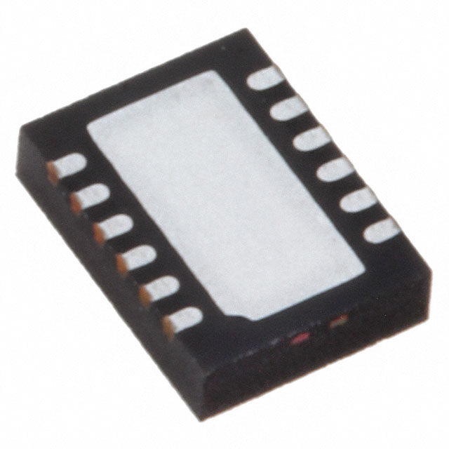
ICGOO电子元器件商城为您提供PD70100ILD-TR由American Microsemiconductor, Inc.设计生产,在icgoo商城现货销售,并且可以通过原厂、代理商等渠道进行代购。 PD70100ILD-TR价格参考¥7.95-¥18.96。American Microsemiconductor, Inc.PD70100ILD-TR封装/规格:PMIC - 以太网供电(PoE) 控制器, Power Over Ethernet Controller 2 Channel 802.3at (PoE+), 802.3af (PoE) 12-DFN (4x3)。您可以下载PD70100ILD-TR参考资料、Datasheet数据手册功能说明书,资料中有PD70100ILD-TR 详细功能的应用电路图电压和使用方法及教程。
Microsemi Corporation(现为Microchip旗下品牌)的PD70100ILD-TR是一款以太网供电(PoE)控制器,主要用于支持IEEE 802.3af/at标准的受电设备(PD)。该芯片广泛应用于需要通过以太网线缆同时传输数据与电力的场景。

典型应用场景包括:

1. IP电话:为企业通信设备提供稳定电源和网络连接。
2. 无线接入点(WAP):为Wi-Fi热点设备远程供电,简化布线。
3. 安防摄像头:特别是网络摄像机(IP Camera),便于安装在无电源插座的位置。
4. 门禁控制系统:为读卡器、控制器等设备提供远程供电。
5. 智能楼宇系统:如传感器、执行器等物联网设备的集中供电管理。

PD70100ILD-TR具备高集成度、低功耗特性,内置浪涌保护和电源管理功能,适用于工业级工作温度范围,适合在复杂环境中稳定运行。
| 参数 | 数值 |
| 产品目录 | 集成电路 (IC) |
| 描述 | IC PD FRONT END 802.3AF/AT 12DFN |
| 产品分类 | PMIC - 以太网供电 (PoE) 控制器 |
| 品牌 | Microsemi Analog Mixed Signal Group |
| 数据手册 | |
| 产品图片 | |
| 产品型号 | PD70100ILD-TR |
| rohs | 无铅 / 符合限制有害物质指令(RoHS)规范要求 |
| 产品系列 | - |
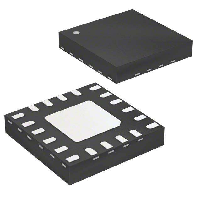
| 供应商器件封装 | 12-DFN(4x3) |
| 其它名称 | PD70100ILD-TRCT |
| 内部开关 | 是 |
| 功率-最大值 | 48W |
| 包装 | 剪切带 (CT) |
| 封装/外壳 | 12-VFDFN 裸露焊盘 |
| 工作温度 | -40°C ~ 85°C |
| 标准 | 802.3at (PoE+), 802.3af (PoE) |
| 标准包装 | 1 |
| 电压-电源 | 0 V ~ 57 V |
| 电流-电源 | 1mA |
| 类型 | 控制器 (PD) |
| 辅助作用 | 无 |
| 通道数 | 2 |


- 商务部:美国ITC正式对集成电路等产品启动337调查
- 曝三星4nm工艺存在良率问题 高通将骁龙8 Gen1或转产台积电
- 太阳诱电将投资9.5亿元在常州建新厂生产MLCC 预计2023年完工
- 英特尔发布欧洲新工厂建设计划 深化IDM 2.0 战略
- 台积电先进制程称霸业界 有大客户加持明年业绩稳了
- 达到5530亿美元!SIA预计今年全球半导体销售额将创下新高
- 英特尔拟将自动驾驶子公司Mobileye上市 估值或超500亿美元
- 三星加码芯片和SET,合并消费电子和移动部门,撤换高东真等 CEO
- 三星电子宣布重大人事变动 还合并消费电子和移动部门
- 海关总署:前11个月进口集成电路产品价值2.52万亿元 增长14.8%


PDF Datasheet 数据手册内容提取
PD70100/PD70200 Datasheet IEEE 802.3af/at PD Front End IC
IEEE 802.3af/at PD Front End IC Contents 1 Revision History ............................................................................................................................. 1 1.1 Revision 3.0 ........................................................................................................................................ 1 1.2 Revision 2.0 ........................................................................................................................................ 1 1.3 Revision 1.1 ........................................................................................................................................ 1 1.4 Revision 1.0 ........................................................................................................................................ 1 1.5 Revision 0.6 ........................................................................................................................................ 1 1.6 Revision 0.5 ........................................................................................................................................ 1 1.7 Revision 0.4 ........................................................................................................................................ 1 1.8 Revision 0.3 ........................................................................................................................................ 1 1.9 Revision 0.1 ........................................................................................................................................ 1 2 Product Overview .......................................................................................................................... 2 2.1 Features .............................................................................................................................................. 2 2.2 Applications ........................................................................................................................................ 2 3 Functional Descriptions ................................................................................................................. 4 3.1 Detail Description ............................................................................................................................... 5 3.1.1 Detection ................................................................................................................................................. 5 3.1.2 Physical Layer Classification .................................................................................................................... 5 3.1.3 Two-Events Detection and AT Flag .......................................................................................................... 5 3.1.4 Soft Start and Inrush Current Protection ................................................................................................ 5 3.1.5 Over-Current Protection ......................................................................................................................... 6 3.1.6 Power Good ............................................................................................................................................. 7 3.1.7 Auxiliary Voltage Output ......................................................................................................................... 7 3.1.8 Thermal Protection ................................................................................................................................. 7 3.1.9 Bulk Capacitor Discharge ......................................................................................................................... 7 4 Electrical Specifications .................................................................................................................. 8 4.1 Absolute Maximum Ratings ................................................................................................................ 8 4.2 Typical Electrical Performance ........................................................................................................... 8 4.2.1 Power Supply ........................................................................................................................................... 8 4.2.2 Detection Mode ...................................................................................................................................... 9 4.2.3 Classification Mode ................................................................................................................................. 9 4.2.4 Mark ...................................................................................................................................................... 10 4.2.5 Isolation Switch ..................................................................................................................................... 10 4.2.6 DC/DC Capacitor Discharger .................................................................................................................. 10 4.2.7 AT_FLAG ................................................................................................................................................ 11 4.2.8 PGOOD .................................................................................................................................................. 11 4.2.9 Thermal Shutdown ................................................................................................................................ 11 Microsemi Proprietary and Confidential. PD70100/PD70200 Datasheet Revision 3.0
IEEE 802.3af/at PD Front End IC 4.2.10 VAUX ................................................................................................................................................... 11 5 Pin Description ............................................................................................................................. 12 6 Package Specifications ................................................................................................................. 13 6.1 Thermal Specifications ..................................................................................................................... 14 7 Ordering Information ................................................................................................................... 15 Microsemi Proprietary and Confidential. PD70100/PD70200 Datasheet Revision 3.0
IEEE 802.3af/at PD Front End IC 1 Revision History 1.1 Revision 3.0 Revision 3.0 was published in January 2018. The following is a summary of changes in revision 3.0 of this document. The formatting of this document was updated to the latest template. MSL level updated. Part marking was updated. For more information, see Ordering Information (see page 15). Absolute Maximum Ratings (see page 8) updated. 1.2 Revision 2.0 Revision 2.0 was published in October 2015. In revision 2.0 of this document, the IC part number was updated from PD70100A to PD70100 (PDN 152044). 1.3 Revision 1.1 Revision 1.1 was published in October 2014. In revision 1.1 of this document, the description of Pin 2 was updated. 1.4 Revision 1.0 Revision 1.0 was published in March 2012. The following is a summary of changes in revision 1.0 of this document. The document address footer was updated. Characteristics were updated. 1.5 Revision 0.6 Revision 0.6 was published in July 2011. In revision 0.6 of this document, the specifiaction was updated. 1.6 Revision 0.5 Revision 0.5 was published in January 2011. In revision 0.5 of this document, the package was updated. 1.7 Revision 0.4 Revision 0.4 was published in December 2010. In revision 0.4 of this document, the package was updated. 1.8 Revision 0.3 Revision 0.3 was published in November 2010. The following is a summary of changes in revision 0.3 of this document. Classification Pulse diagrams were added. Catalog numbers metrology was changed. Extensive changes were made to document format and Theory of Operation section. Package drawing was corrected. Product Highlight and Typical Characteristics were added. 1.9 Revision 0.1 Revision 0.1 was published in April 2010. It was the first publication of this document. Microsemi Proprietary and Confidential. PD70100/PD70200 Datasheet Revision 3.0 1
IEEE 802.3af/at PD Front End IC 2 Product Overview The PD70100 and PD70200 devices are part of Microsemi’s series of Power over Ethernet (PoE) Powered Devices chips (PD). The PD70100 and PD70200 devices transmit integrated power and analog data in a single 12-pin package. They are used in Powered Devices (PD), thus enabling next generation network devices to share power and data over the same cable. Microsemi’s new PD family offers a solution to any PD application compliant with IEEE802.3af and IEEE802.3at standards and 4-pairs extra power applications. The IC family’s components can be used in both indoor and outdoor applications. The device family meets all PD-side-standards such as: Detection Classification Integrated isolation switch with inrush current limiter, and over-current protection Two-events classification recognition and AT flag generation (PD70200 only). In addition, the devices have a discharge mechanism for a DC/DC input capacitor, ensuring quick redetection capability in case the RJ-45 plug is disconnected and reconnected within a short time span. PD70200 IC design specifically supports IEEE802.3at standard, including two events classification detection that enables the PD to distinguish whether the connected power source equipment (PSE) is IEEE802.3at or IEEE802.3af based. The PD70100/PD70200 ICs are designed to support 4 pair applications for PDs that require higher power. 2.1 Features Designed to Support IEEE802.3af and IEEE802.3at standards PD Detection & Programmable Classification Signature Two-events Classification Flag Signature Resistor Disconnection after Detection Integrated 0.6 Ω Isolating Switch and Inrush Current Limiter. 4-pairs support with a single PD70200 IC for up to 48 W 4-pairs support with two PD70200 ICs for up to 96 W Less than 10 µA Offset Current during Detection Single DC Voltage Input (37 V – 57 V) Wide Operating Temperature Range: −40 to 85 °C On-chip Thermal Protection 12-pin 3 × 4mm Package RoHS Compliant MSL3 2.2 Applications Power over Ethernet Powered Devices IEEE802.3af & at 10/100/1000 BASE-T 4-pair extra power applications Indoor and outdoor applications The following illustration shows a typical PD70100 /PD70200 application. Microsemi Proprietary and Confidential. PD70100/PD70200 Datasheet Revision 3.0 2
IEEE 802.3af/at PD Front End IC Figure 1 • Typical Application with IEEE802.3at PSE Microsemi Proprietary and Confidential. PD70100/PD70200 Datasheet Revision 3.0 3
IEEE 802.3af/at PD Front End IC 3 Functional Descriptions The following illustration shows the functional blocks of the PD70100. Figure 2 • PD70100 Functional Block Diagram The following illustration shows the functional blocks of the PD70200. Figure 3 • PD70200 Functional Block Diagram Microsemi Proprietary and Confidential. PD70100/PD70200 Datasheet Revision 3.0 4
IEEE 802.3af/at PD Front End IC 3.1 Detail Description PD70100/PD70200 IC provides IEEE 802.3af/at compliant PD Front-End functions including Detection, Physical Layer Classification, Two-Events Classification (PD70200 only), Auxiliary Voltage Output, Power Good, Soft Start Current Limiting, Over-Current Protection, and Bulk Capacitor Discharge. 3.1.1 Detection IEEE 802.3af/at compliant detection is provided by a 24.9 KΩ resistor connected between V and R PP DET pin. R pin is connected to VPN via an open drain MOSFET with a maximum specified RDS of 50 Ω. DET IN ON Internal logic monitors V to VPN and connects the R pin to VPN when the rising V to VPN PP IN DET IN PP IN voltage is between 2.5 V and 10.1 V. When rising V to VPN voltage exceeds 10.1 V, the MOSFET is PP IN switched off. Once above 10.1 V, falling V to VPN voltage between 2.45 V and 4.85 V will reconnect PP IN R pin to VPN . DET IN 3.1.2 Physical Layer Classification Physical Layer (hardware) Classification per IEEE 802.3af/at is generated via a regulated reference voltage of 1.2 V, switched onto the R pin. Internal logic monitors the V to VPN voltage and CLASS PP IN connects the 1.2 V reference to R pin at a rising V to VPN voltage threshold between 11.1 V and CLASS PP IN 13.5 V. Once V to VPN has exceeded the rising threshold, there is a 1 V minimum hysteresis between PP IN the V rising (turn-on) threshold and the V falling (turn-off) threshold. PP PP The 1.2 V reference stays connected to the R pin until the V to VPN rising voltage exceeds the CLASS PP IN upper turn-off threshold of 20.9 V to 23.9 V. The 1.2 V reference voltage is disconnected from the R CLASS pin at V to VPN voltages above the upper threshold. PP IN Classification current signature is provided via a resistor connected between R pin and VPN . The CLASS IN classification current is therefore the current drawn by the PD70100/PD70200 IC during the classification phase, and is simply the 1.2 V reference voltage divided by the R resistor value. The CLASS maximum current available at the R pin is current limited to 55 mA (typical). CLASS 3.1.3 Two-Events Detection and AT Flag The PD70200 IC provides IEEE 802.3at Type 2 compliant detection of the “Two Events Classification Signature”, and generation of the AT flag. This feature is available on the PD70200 IC only. Simply put, the “Two Events Classification Signature” is a means by which an IEEE 802.3at Type 2 Power Source can inform a compliant Power Device (PD) that it is AT Type 2 compliant, and as such is capable of providing AT Type 2 power levels. The Power Source communicates with a Type 2 compliant signature by toggling the V to VPN voltage PP IN twice (2 “events”) during the Physical Layer Classification phase. The V to VPN voltage is toggled from PP IN the Physical Layer Classification’s voltage level (13.5 V to 20.9 V) down to a voltage “Mark” level. Voltage “Mark” level is specified as a V to VPN voltage of 4.9 V to 10.1 V. PP IN PD70200 IC recognizes a V to VPN falling edge from Classification level to Mark level as being one PP IN event of the Two-Events Signature. If two such falling edges are detected, PD70200 will assert AT flag by means of an open drain MOSFET connected between AT_FLAG pin and VPN . OUT AT_FLAG pin is active low; a low impedance state between AT_FLAG and VPN indicates a valid Two- OUT Events Classification Signature was received, and the Power Source is AT Type 2 compliant. AT_FLAG MOSFET is capable of 5 mA of current and can be pulled up to V . PP 3.1.4 Soft Start and Inrush Current Protection PD70100/PD70200 IC contains an internal isolation switch, that provides ground isolation between Power Source and PD application during Detection and Classification phases. The isolation switch is a N- channel MOSFET, wired in a common source configuration where the MOSFET’s Source is connected to Power Source ground at VPN , and the MOSFET’s Drain is connected to application’s primary ground at IN VPN . OUT Internal logic monitors V to VPN voltage and keeps the MOSFET in a high impedance state until V to PP IN PP Microsemi Proprietary and Confidential. PD70100/PD70200 Datasheet Revision 3.0 5
IEEE 802.3af/at PD Front End IC Internal logic monitors V to VPN voltage and keeps the MOSFET in a high impedance state until V to PP IN PP VPN voltage reaches turn-on threshold of 36 V to 42 V. Once V to VPN voltage exceeds this IN PP IN threshold, the MOSFET is switched into one of two modes. The mode into which the MOSFET is switched is determined by the voltage developed across the MOSFET, or put another way, the VPN to VPN differential voltage. Two modes are defined below: OUT IN Table 1 • Isolation Switch Modes VPNOUT to VPNIN Mode Description > 0.7 V Soft Start Mode Limits VPNOUT current to 240 mA (typical) ≤ 0.7 V Normal Operating Mode Limits VPNOUT current to 1.8 A (typical) By controlling the MOSFET current based on VPN to VPN voltage, inrush currents generated by fully OUT IN discharged bulk capacitors can be limited. This method limits current to a maximum of 350 mA, compliant with IEEE 802.3af/at specification. Soft Start current limiting is required to reduce occurrences of voltage sag at the PD input during device power-up. A comparison is shown in the figure below. Once bulk capacitance has charged up to a point where VPN to VPN differential voltage is less than OUT IN 0.7 V, the isolation MOSFET is switched into normal operating mode with MOSFET current limit set at 1.8 A (typical), to provide over-current protection. PD70100 and PD70200 ICs are different in their respective isolation MOSFET’s continuous current handling capability: PD70100: 450 mA (max.) PD70200: 1123 mA (max.) An adequate heat sink for the PD70100/PD70200 IC’s exposed pad must be provided to achieve these current levels without damaging the IC. A large, heavy copper fill area and/or a heavy ground plane with Thermal Vias is recommended. Electrically the exposed pad ground plane should be connected to VPN IN. Internal logic monitoring V to VPN will place the isolation switch MOSFET in a high impedance state if PP IN voltage between V and VPN drops below 31 V to 34 V. PP IN 3.1.5 Over-Current Protection Over-current protection is provided on the PD70100/PD70200 IC using the Isolation MOSFET Switch, which limits the VPN current to 1.8 A during normal operation. See previous description of Soft Start. OUT Microsemi Proprietary and Confidential. PD70100/PD70200 Datasheet Revision 3.0 6
IEEE 802.3af/at PD Front End IC 3.1.6 Power Good During Soft Start mode, the PD70100/PD70200 IC monitors VPN to VPN differential voltage. When OUT IN this voltage is less than 0.7 V (max.), the IC enters normal operation mode and the isolation switch current limit is increased to 1.8 A (typical). At this same 0.7 V (max.) threshold the Power Good signal is asserted by means of an open drain MOSFET between PGOOD and VPN . OUT PGOOD pin is active low; a low impedance state between PGOOD and VPN indicates the Soft Start OUT mode has finished and the isolation switch has transitioned into normal operating mode. PGOOD MOSFET can handle current of 5 mA and can be pulled up to V . PP 3.1.7 Auxiliary Voltage Output PD70100/PD70200 IC provides a 10.5 V (typical) regulated output to be used as a start-up supply for DC /DC controllers whose V is provided via a bootstrap winding. This regulated supply is available at V CC AUX pin, and is referenced to VPN pin. V supply is designed for low-duty operation, and should not be OUT AUX designed as a primary housekeeping supply. The current capability is continuous 2 mA, with 10 mA peak (≤ 10 ms). V output is current-limited at 10 mA (min.). AUX For stability, the V regulator requires a minimum of 4.7 µF ceramic capacitor connected directly AUX between V and VPN pins. AUX OUT 3.1.8 Thermal Protection Both PD70100 and PD70200 IC include temperature sensors which individually monitor both the isolation MOSFET and the Classification Current Source for over temperature conditions. In case of an over temperature condition, the sensor will activate protection circuitry which will disconnect its respective monitored function. 3.1.9 Bulk Capacitor Discharge The bulk capacitor discharge circuitry eliminates the need to place a diode in series with the V line to PP prevent an application’s bulk capacitance from discharging through the detection resistor and the isolation switch MOSFET’s body diode. Discharge current through the detection resistor can cause failure of the detection signature in cases where a PD is connected and the bulk capacitance is not fully discharged. During normal operation, PD70100/PD70200 IC continuously monitors voltage at V to VPN . Should V PP IN PP to VPN voltage fall below isolation switch turn-off threshold (31 V to 34 V), isolation switch MOSFET is IN immediately placed in a high-impedance state. At this point the internal logic monitors the voltage at V PP to VPN . If V to VPN voltage is between 1.5 V to 32 V, a 23 mA (min.) constant current source is OUT PP OUT connected across the V and VPN pins. This constant current source provides bulk capacitor PP OUT discharge. A 220 µF bulk capacitance can be discharged from 32 V to 1.5 V in a maximal period of 292 ms. Microsemi Proprietary and Confidential. PD70100/PD70200 Datasheet Revision 3.0 7
IEEE 802.3af/at PD Front End IC 4 Electrical Specifications 4.1 Absolute Maximum Ratings Table 2 • Absolute Maximum Ratings Supply Input Voltage (VPP) Continuous −0.3 V to 74 VDC Supply Input Voltage (VPP) 1 ms pulse −0.3 V to 88 VDC Port Negative Out Voltage (VPNOUT) −0.3 V to 74 VDC RDET Continuous −0.3 V to 74 VDC RDET 1 mS pulse −0.3 V to 88 VDC RCLASS, RREF −0.3 V to 5 VDC VAUX −0.3 V to 30 VDC PGOOD, AT_FLAG (with respect to VPNOUT) Continuous −0.3 V to 74 VDC PGOOD, AT_FLAG (with respect to VPNOUT) 1 mS pulse −0.3 V to 88 VDC ESD Protection* ±1.5 kV HBM Maximum Operating Junction Temperature (TA) 150 °C Operating Ambient Temperature −40 °C to 85 °C Storage Temperature Range −65 °C to 150 °C Peak Package Solder Reflow Temp (40 seconds max exposure) 260 °C * All pins except pin 11 (V ). Pin 11 ESD Protection ±150 V HBM. AUX ** No pin voltage can be higher than Vpp. Note: Exceeding these ratings could cause damage to the device. All voltages are with respect to VPN IN except for Vaux, PGOOD and AT_FLAG with respect to VPN . Currents are positive into, negative out of OUT specified terminal. These are stress ratings only and functional operation of the device at these or any other conditions beyond those indicated under “Recommended Operating Conditions” are not implied. Exposure to “Absolute Maximum Ratings” for extended periods may affect device reliability. 4.2 Typical Electrical Performance Unless otherwise specified, the following specifications apply over the operating ambient temperature −40 °C ≤ T ≤ 85 °C. Production tests are done at 25 °C T . AMB A 4.2.1 Power Supply Table 3 • Power Supply Parameter Symbol Min Typ Max Units Test Conditions/Comment Input Voltage VPP 0 55 57 V Supports Full IEEE802.3 af/at functionality Power Supply Current at Operating 1 3 mA VPP = 55 V Mode Microsemi Proprietary and Confidential. PD70100/PD70200 Datasheet Revision 3.0 8
IEEE 802.3af/at PD Front End IC 4.2.2 Detection Mode Table 4 • Detection Mode Parameter Symbol Min Typ Max Units Test Conditions/Comment Detection is connected. DETRANGE 1.3 10.1 V Measured between VPP and VPNIN At this voltage range RDET must be on. Detection Switch ON Resistance RDET-on 50 Ω 2.5 V ≤ (ΔVPP to VPNIN) ≤ 10.1 V PD-detection Measured between RDET and VPNIN Detection is Disconnected RDET-off 10.1 12.8 V Measured between VPP and VPNIN Detection Switch OFF Resistance RDET-off 2.0 MΩ 12.8 V ≤ (ΔVPP to VPNIN) ≤ 57.0 V Measured between RDET and VPNIN Input Offset Current IOFFSET 16 μA 1.1 V to 10.1 V −40 °C ≤ TJ ≤ 85 °C IOFFSET 10 μA 1.1V to 10.1V −40 °C ≤ TJ ≤ 55 °C 4.2.3 Classification Mode Table 5 • Classification Mode Parameter Symbol Min Typ Max Units Test Conditions/Comment Classification Current Source, Turn ON VTH- 11.4 13.7 V Turn on for any ICLASS while ThresholdRangeMeasured at VPP low-on VPP increases Classification Current Source, Turn OFF VTH- 20.9 23.9 V Turn off while VPP ThresholdRangeMeasured at VPP high- increases off Current Limit Threshold ICLASS- 50.0 68 80.0 mA LIM Input Current IPP When Classification ICLASS- 4.0 mA Class 0 Function is Disabled DIS RCLASS = Disconnect Input Current IPP When Classification ICLASS- 9.0 10.5 12.0 mA Class 1 Function is Enabled EN RCLASS = 133 Ω ± 1% 17.0 18.5 20.0 mA Class 2 RCLASS = 69.8 Ω ± 1% 26.0 28.0 30.0 mA Class 3 RCLASS = 45.3 Ω ± 1% 36.0 40.0 44.0 mA Class 4 RCLASS = 30.9 Ω ± 1% Microsemi Proprietary and Confidential. PD70100/PD70200 Datasheet Revision 3.0 9
IEEE 802.3af/at PD Front End IC 4.2.4 Mark Table 6 • Mark Parameter Symbol Min Typ Max Units Test Conditions/Comment Mark, Working Voltage Range VMARK 4.9 10.1 V When voltage decreases Measured between VPP to VPNIN Mark Current IMARK 0.25 4 mA Chip current 4.2.5 Isolation Switch Table 7 • Isolation Switch Parameter Symbol Min Typ Max Units Test Conditions/Comment Isolation Switch MOSFET Switches VSW-START 36 42 V from Off to ILIM-LOW Isolation Switch MOSFET Switched VSW-OFF 30.5 34.5 V Off Startup Current Limit, ILIM ILIM-LOW 105 240 325 mA VPNIN to VPNOUT Threshold Voltage VDIFF 0.7 V When VPNIN to VPNOUT ≤ VDIFF for ILIM- LOW to ILIM-HIGH Switchover , Isolating switch switches over from ILIM-LOW to ILIM-HIGH. Over Current Protection Current OCP 1500 1800 2000 mA Limit Continuous Operation Load ILOAD 350 450 mA Isolating switch at ILIM-HIGH Current (PD70100) Continuous Operation Load 600 1123 Current (PD70200) Continuous Operation Total RDSON SW-RDSON 0.6 Ω Total resistance between VPNIN and VPNOUT Isolating switch at ILIM-HIGH 4.2.6 DC/DC Capacitor Discharger Table 8 • DC/DC Capacitor Discharger Parameter Symbol Min Typ Max Units Test Conditions /Comment DC/DC Input Capacitance 220 µF For reference only Guaranteed by design (not tested in production) Discharge Current 22.8 32 50 mA 7.0V ≤ VPP to VPNOUT ≤ 30 V Full Discharge Time for Full Discharge of Input TDSC 500 ms VPP < UVLO threshold Capacitance Guaranteed by design (not tested in production) Microsemi Proprietary and Confidential. PD70100/PD70200 Datasheet Revision 3.0 10
IEEE 802.3af/at PD Front End IC 4.2.7 AT_FLAG Table 9 • AT_FLAG Parameter Symbol Min Typ Max Units Test Conditions/Comment Output Low Voltage 0.4 V IOL = 0.75 mA 2.5 V IOL MAX = 5 mA Leakage Current 1.7 µA VATFLAG = 57 V 4.2.8 PGOOD Table 10 • PGOOD Parameter Symbol Min Typ Max Units Test Conditions/Comment Output Low Voltage 0.4 µF IOL = 0.75 mA 2.5 mA IOL MAX = 5 mA Leakage Current 1.7 µA VPGOOD = 57 V 4.2.9 Thermal Shutdown Table 11 • Thermal Shutdown Parameter Symbol Min Typ Max Units Test Conditions/Comment Thermal Shutdown Temperature 180 200 220 °C 4.2.10 VAUX Reference to VPN . OUT Table 12 • VAUX Parameter Symbol Min Typ Max Units Test Conditions/Comment VAUX Output Voltage On VAUX-on 9.5 10.5 11.8 V Isolating switch at ILIM-HIGH and PGOOD = Low Output Current Peak IVAUXP 0 10 mA Capacitor = 30 µF When TLOAD ≤ 5 mS Isolating switch at ILIM-HIGH and PGOOD = Low Output Continuous IVAUXC 0 2 mA When TLOAD ≤ 10 mS Current Isolating switch at ILIM-HIGH and PGOOD = Low VAUX Output Current IVAUX 10 32 mA Isolating switch at ILIM-HIGH and PGOOD = Limit Low Microsemi Proprietary and Confidential. PD70100/PD70200 Datasheet Revision 3.0 11
IEEE 802.3af/at PD Front End IC 5 Pin Description The following illustration shows the device pinout, from the top view and bottom view. Figure 4 • Pinout Top View and Bottom View The following table lists the pin descriptions for the PD70100/PD70200 devices. Table 13 • Pin Descriptions Pin Pin Name Pin Name Type Description (PD70100) (PD70200) 1 RDET RDET Valid Detection resistor. Connect external 24.9 KΩ detection resistor between RDET and VPP. 2 RREF RREF Bias current resistor. Connect a 243 k 1% resistor between this pin and VPNIN. 3 RCLASS RCLASS Power classification setting. Connect external class resistor between R CLASS and VPNIN. 4 VPNIN VPNIN Power VPort Negative input. Connected to the isolating SW input. N-channel MOSFET source. The exposed thermal pad should be connected to 5 these pins. 6 N.C. N.C. 7 VPNOUT VPNOUT Power Vport Negative output. Connected to the isolating SW output. N- /Gnd channel MOSFET Drain. Primary side Ground. 8 A decent ground plane should be deployed around this pin whenever is possible. 9 N.C AT_FLAG Open The two-event detector should discern between AF and AT drain classification waveforms and outputs the AT_FLAG (PD70200 only). 10 PGOOD PGOOD Open After startup, a PGOOD flag is generated in order to optionally inform drain the application DC/DC converter that the power rails are ready. 11 VAUX VAUX Power Auxiliary output voltage to VPNOUT. Can be used for DC-DC startup for bootstrap initiation. 12 VPP VPP Power High voltage positive input, reference to VPNIN and high voltage positive input, reference to VPNOUT during capacitor discharge. EP EPAD EPAD Connect to VPNIN. EPAD should be connected to a large copper area for improved thermal management. Microsemi Proprietary and Confidential. PD70100/PD70200 Datasheet Revision 3.0 12
IEEE 802.3af/at PD Front End IC 6 Package Specifications This section provides information about the available package. Note: Dimensions do not include mold flash or protrusions; these shall not exceed 0.155 mm (.006”) on any side. Lead dimension shall not include solder coverage. Dimensions are in millimeters, inches for reference only. Figure 5 • Package Drawing Dimensions and Measurements Table 14 • Package Dimensions: DFN Dimension Millimeters Inches Min Max Min Max A 0.80 1.00 0.031 0.039 A1 0.00 0.05 0.000 0.002 A3 0.20 REF 0.008 REF D 4.00 BSC 0.157 BSC E 3.00 BSC 0.118 BSC D2 3.00 3.70 0.118 0.146 E2 1.40 1.80 0.055 0.071 e 0.50 BSC 0.0197 BSC K 0.20 MIN 0.008 MIN L 0.30 0.50 0.012 0.020 b 0.18 0.30 0.007 0.012 Microsemi Proprietary and Confidential. PD70100/PD70200 Datasheet Revision 3.0 13
IEEE 802.3af/at PD Front End IC 6.1 Thermal Specifications The following table lists the thermal specifications for the PD70100 and PD70200 devices. Table 15 • Thermal Specifications Parameter Value Typical thermal resistance: junction to ambient 40 °C/W Typical thermal resistance: junction to case 4 °C/W The θ numbers are guidelines for the thermal performance of the device/pc-board system. All JA specifications assume no ambient airflow. Microsemi Proprietary and Confidential. PD70100/PD70200 Datasheet Revision 3.0 14
IEEE 802.3af/at PD Front End IC 7 Ordering Information Table 16 • Ordering Information Part Number Packaging Package Part Marking Type PD70100ILD Bulk MSC DFN PD70100ILD-TR Tape and 70100 Reel 4 mm × 3 mm F R e31 12 pins YYWWAZZ2 RoHS Compliant / Pb-free PD70200ILD Bulk MSC DFN PD70200ILD-TR Tape and 70200 Reel 4 mm × 3 mm F R e31 12 pins RoHS Compliant / YYWWAZZ2 Pb-free 1. F R e3: F = FAB Code, R = Product revision code, and e3 = 2nd level interconnect. 2. YY = Year, WW = Week, A = Assembly location, and ZZ = Assembly Lot sequence code. Microsemi Proprietary and Confidential. PD70100/PD70200 Datasheet Revision 3.0 15
IEEE 802.3af/at PD Front End IC Microsemi makes no warranty, representation, or guarantee regarding the information contained herein or the suitability of its products and services for any particular purpose, nor does Microsemi assume any liability whatsoever arising out of the application or use of any product or circuit. The products sold hereunder and any other products sold by Microsemi have been subject to limited testing and should not be used in conjunction with mission-critical equipment or applications. Any performance specifications are believed to be reliable but are not verified, and Buyer must conduct and complete all performance and other testing of the products, alone and together with, or installed in, any end-products. Buyer shall not rely on any data and performance specifications or parameters provided by Microsemi. It is the Buyer's responsibility to independently determine suitability of any Microsemi Corporate Headquarters products and to test and verify the same. The information provided by Microsemi hereunder is provided "as is, where is" and with all faults, and the One Enterprise, Aliso Viejo, entire risk associated with such information is entirely with the Buyer. Microsemi does not grant, explicitly or implicitly, to any party any patent rights, CA 92656 USA licenses, or any other IP rights, whether with regard to such information itself or anything described by such information. Information provided in this Within the USA: +1 (800) 713-4113 document is proprietary to Microsemi, and Microsemi reserves the right to make any changes to the information in this document or to any products Outside the USA: +1 (949) 380-6100 and services at any time without notice. Fax: +1 (949) 215-4996 Email: sales.support@microsemi.com Microsemi Corporation (Nasdaq: MSCC) offers a comprehensive portfolio of semiconductor and system solutions for aerospace & defense, www.microsemi.com communications, data center and industrial markets. Products include high-performance and radiation-hardened analog mixed-signal integrated © 2010–2017 Microsemi Corporation. All rights reserved. Microsemi and circuits, FPGAs, SoCs and ASICs; power management products; timing and synchronization devices and precise time solutions, setting the world's the Microsemi logo are trademarks of Microsemi Corporation. All other standard for time; voice processing devices; RF solutions; discrete components; enterprise storage and communication solutions; security technologies trademarks and service marks are the property of their respective owners. and scalable anti-tamper products; Ethernet solutions; Power-over-Ethernet ICs and midspans; as well as custom design capabilities and services. Microsemi is headquartered in Aliso Viejo, California, and has approximately 4,800 employees globally. Learn more at www.microsemi.com. PD-000303241 Microsemi Proprietary and Confidential. PD70100/PD70200 Datasheet Revision 3.0 16