ICGOO在线商城 > 集成电路(IC) > 接口 - 驱动器,接收器,收发器 > MAX3320TCAP+

 Datasheet下载
- 型号: MAX3320TCAP+
- 制造商: Maxim
- 库位|库存: xxxx|xxxx
- 要求:
| 数量阶梯 | 香港交货 | 国内含税 |
| +xxxx | $xxxx | ¥xxxx |
查看当月历史价格
查看今年历史价格
MAX3320TCAP+产品简介:
ICGOO电子元器件商城为您提供MAX3320TCAP+由Maxim设计生产,在icgoo商城现货销售,并且可以通过原厂、代理商等渠道进行代购。 MAX3320TCAP+价格参考。MaximMAX3320TCAP+封装/规格:接口 - 驱动器,接收器,收发器, 全 收发器 2/2 RS232 20-SSOP。您可以下载MAX3320TCAP+参考资料、Datasheet数据手册功能说明书,资料中有MAX3320TCAP+ 详细功能的应用电路图电压和使用方法及教程。
Maxim Integrated的MAX3320TCAP+是一款低功耗、单通道RS-232接口IC,属于接口驱动器、接收器、收发器类别。该芯片主要应用于需要串行通信的嵌入式系统和工业控制设备中,适用于数据传输速率高达120kbps的场景。

其典型应用场景包括工业自动化设备、测试测量仪器、手持终端、POS机、通信模块等。MAX3320TCAP+采用专有的低电压差分信号技术(ForteCAP™),可有效减小PCB面积并提高集成度,同时具备较高的抗干扰能力和稳定性,适合在复杂电磁环境中使用。

此外,该芯片支持1.65V至3.6V宽电源电压范围,具备自动关机和唤醒功能,有助于降低系统功耗,适用于电池供电设备。其内部集成电荷泵,可提供符合RS-232标准的电压电平,简化了外围电路设计。

总结而言,MAX3320TCAP+广泛应用于需要可靠串口通信、低功耗及小尺寸设计要求的工业与消费类电子产品中。
| 参数 | 数值 |
| 产品目录 | 集成电路 (IC)半导体 |
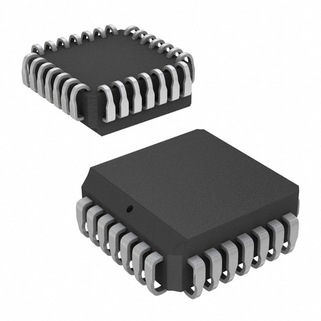
| 描述 | IC TXRX RS232 250KBPS 20-SSOPRS-232接口集成电路 3-5.5V 250kbps Transceiver |
| 产品分类 | |
| 品牌 | Maxim Integrated |
| 产品手册 | |
| 产品图片 |
|
| rohs | 符合RoHS无铅 / 符合限制有害物质指令(RoHS)规范要求 |
| 产品系列 | 接口 IC,RS-232接口集成电路,Maxim Integrated MAX3320TCAP+- |
| 数据手册 | |
| 产品型号 | MAX3320TCAP+ |
| 产品培训模块 | http://www.digikey.cn/PTM/IndividualPTM.page?site=cn&lang=zhs&ptm=25703http://www.digikey.cn/PTM/IndividualPTM.page?site=cn&lang=zhs&ptm=25705 |
| 产品目录页面 | |
| 产品种类 | RS-232接口集成电路 |
| 传播延迟时间ns | 0.3 us |
| 供应商器件封装 | 20-SSOP |
| 关闭 | Yes |
| 功能 | Transceiver |
| 包装 | 管件 |
| 协议 | RS232 |
| 双工 | 全 |
| 商标 | Maxim Integrated |
| 安装类型 | 表面贴装 |
| 安装风格 | SMD/SMT |
| 封装 | Tube |
| 封装/外壳 | 20-SSOP(0.209",5.30mm 宽) |
| 封装/箱体 | SSOP-20 |
| 工作温度 | 0°C ~ 70°C |
| 工作温度范围 | 0 C to + 70 C |
| 工作电源电压 | 3 V to 5.5 V |
| 工厂包装数量 | 66 |
| 应用说明 | |
| 接收器滞后 | 300mV |
| 接收机数量 | 2 Receiver |
| 数据速率 | 250 kb/s |
| 最大工作温度 | + 70 C |
| 最小工作温度 | 0 C |
| 标准包装 | 1 |
| 激励器数量 | 2 Driver |
| 电压-电源 | 3 V ~ 5.5 V |
| 电源电流 | 1 mA |
| 类型 | 收发器 |
| 系列 | MAX3320T |
| 输入/输出端数量 | 8 |
| 零件号别名 | MAX3320T |
| 驱动器/接收器数 | 2/2 |


- 商务部:美国ITC正式对集成电路等产品启动337调查
- 曝三星4nm工艺存在良率问题 高通将骁龙8 Gen1或转产台积电
- 太阳诱电将投资9.5亿元在常州建新厂生产MLCC 预计2023年完工
- 英特尔发布欧洲新工厂建设计划 深化IDM 2.0 战略
- 台积电先进制程称霸业界 有大客户加持明年业绩稳了
- 达到5530亿美元!SIA预计今年全球半导体销售额将创下新高
- 英特尔拟将自动驾驶子公司Mobileye上市 估值或超500亿美元
- 三星加码芯片和SET,合并消费电子和移动部门,撤换高东真等 CEO
- 三星电子宣布重大人事变动 还合并消费电子和移动部门
- 海关总署:前11个月进口集成电路产品价值2.52万亿元 增长14.8%


PDF Datasheet 数据手册内容提取
19-1253; Rev 0; 8/97 3V to 5.5V, up to 250kbps True RS-232 Transceiver with 4µA AutoShutdown Plus and Power-On Reset _______________General Description ____________________________Features M The MAX3320 combines a microprocessor (µP) super- 'Precise Monitoring of 5V and 3.3V Power- A visory circuit with an RS-232 transceiver. The power-on Supply Voltages: X reset performs a single function: it asserts a reset signal — 100ms (min) Power-On RESETPulse Width whenever the VCC supply voltage declines below a pre- 3 — Power-Supply Transient Immunity set threshold, staying asserted for at least 100ms after 3 VCC rises above the reset threshold. The MAX3320 has — Guaranteed RESETValid to VCC= 1V 2 an active-low RESEToutput, which is guaranteed to be in '4µA Supply Current Achieved with 0 the correct state for VCCdown to 1V. The reset compara- AutoShutdown Plus tor is designed to ignore fast transients on VCC. Reset A thresholds suitable for operation with a variety of supply 'Receivers Always Active / B voltages are available. 'Power-On Reset Always Active / The MAX3320 transceivers have a proprietary low- '4µA Low-Power Shutdown L dropout transmitter output stage, enabling true RS-232 / performance with a dual charge pump powered from a '250kbps Guaranteed Data Rate T +3V to +5.5V supply. The device requires only four small 0.1µF external charge-pump capacitors, and is guaranteed to run at data rates of up to 250kbps. It comes in the space-saving 20-pin SSOP package. ________________________Applications ______________Ordering Information Palmtop Computers PART* TEMP. RANGE PIN-PACKAGE Portable/Battery-Powered Equipment MAX3320_CAP 0°C to +70°C 20 SSOP Hand-Held Equipment MAX3320_EAP -40°C to +85°C 20 SSOP Peripherals *This part offers a choice of reset threshold voltage. From the Printers table below, select the suffix corresponding to the desired threshold and insert it into the blank to complete the part number. __________________Pin Configuration RESET THRESHOLD SUFFIX (V) A 4.25 TOP VIEW B 2.85 V+ 1 20 C1+ L 4.63 C2+ 2 19 VCC T 3.08 C2- 3 18 C1- V- 4 17 GND MAX3320 T1IN 5 MAXxxx 16 T1OUT T2IN 6 15 T2OUT Typical Operating Circuit appears at end of data sheet. R1OUT 7 14 R1IN R2OUT 8 13 R2IN INVALID 9 12 FORCEON RESET 10 11 FORCEOFF SSOP AutoShutdown Plus is a trademark of Maxim Integrated Products. ________________________________________________________________Maxim Integrated Products 1 For free samples & the latest literature: http://www.maxim-ic.com, or phone 1-800-998-8800. For small orders, phone 408-737-7600 ext. 3468.
3V to 5.5V, up to 250kbps True RS-232 Transceiver with 4µA AutoShutdown Plus and Power-On Reset T ABSOLUTE MAXIMUM RATINGS / L VCC.............................................................................-0.3V to 6V Short-Circuit Duration V+ (Note 1).................................................................-0.3V to 7V T_OUT....................................................................Continuous / B V- (Note 1)...................................................................0.3V to -7V Continuous Power Dissipation (TA= +70°C) V+ + |V-|(Note 1)...................................................................13V SSOP (derate 8.00mW/°C above +70°C)....................640mW / A Input Voltages Operating Temperature Ranges T_IN, FORCEOFF, FORCEON................................-0.3V to 6V MAX3320_CAP...................................................0°C to +70°C 0 R_IN.................................................................................±25V MAX3320_EAP................................................-40°C to +85°C 2 Output Voltages Storage Temperature Range.............................-65°C to +160°C T_OUT..........................................................................±13.2V Lead Temperature (soldering, 10sec).............................+300°C 3 R_OUT, INVALID, RESET.......................-0.3V to (VCC+ 0.3V) 3 Note 1:V+ and V- can have a magnitude of +7V (max), but their absolute difference cannot exceed +13V. X Stresses beyond those listed under “Absolute Maximum Ratings” may cause permanent damage to the device. These are stress ratings only, and functional A operation of the device at these or any other conditions beyond those indicated in the operational sections of the specifications is not implied. Exposure to absolute maximum rating conditions for extended periods may affect device reliability. M ELECTRICAL CHARACTERISTICS (VCC= 3V to 5.5V, C1–C4 = 0.1µF (tested at 3.3V ±10%), C1 = 0.047µF, C2–C4 = 0.33µF (tested at 5V ±10%), TA= TMINto TMAX, unless otherwise noted. Typical values are at TA= +25°C.) PARAMETER CONDITIONS MIN TYP MAX UNITS DC CHARACTERISTICS Power-Supply Current No load, VCC= 3.3V or 5V, TA= +25°C 0.45 1.0 mA Shutdown Supply Current FORCEOFF= GND, TA= +25°C 4.0 10 µA AutoShutdown Plus All R_IN unconnected, FORCEON = GND, 4.0 10 µA Supply Current FORCEOFF= VCC, all T_IN = VCCor GND, TA= +25°C LOGIC INPUTS AND RECEIVER OUTPUTS Input Logic Threshold Low T_IN, FORCEON, FORCEOFF 0.8 V T_IN, FORCEON, VCC= 3.3V 2.0 Input Logic Threshold High V FORCEOFF VCC= 5V 2.4 Input Leakage Current T_IN, FORCEON, FORCEOFF ±0.01 ±1.0 µA Input Hysteresis T_IN, FORCEON, FORCEOFF 250 mV Output Voltage Low IOUT= 1.6mA 0.4 V VCC- VCC - Output Voltage High IOUT= -1mA V 0.6 0.1 RECEIVER INPUTS Input Voltage Range -25 25 V VCC= 3.3V 0.6 1.2 Input Threshold Low V VCC= 5V 0.8 1.5 VCC= 3.3V 1.5 2.4 Input Threshold High V VCC= 5V 1.8 2.4 Input Hysteresis 0.3 V Input Resistance TA= +25°C 3 5 7 kW INVALIDOUTPUT Receiver Input Threshold to Figure 3, positive threshold 2.7 V INVALIDOutput High Figure 3, negative threshold -2.7 Receiver Input Threshold to Figure 3 -0.3 0.3 V INVALIDOutput Low INVALIDOutput Voltage Low IOUT= 1.6mA 0.4 V 2 _______________________________________________________________________________________
3V to 5.5V, up to 250kbps True RS-232 Transceiver with 4µA AutoShutdown Plus and Power-On Reset ELECTRICAL CHARACTERISTICS (continued) M (VCC= 3V to 5.5V, C1–C4 = 0.1µF (tested at 3.3V ±10%), C1 = 0.047µF, C2–C4 = 0.33µF (tested at 5V ±10%), TA= TMINto TMAX, A unless otherwise noted. Typical values are at TA= +25°C.) X PARAMETER CONDITIONS MIN TYP MAX UNITS 3 INVALIDOutput Voltage High IOUT= -1mA VCC- 0.6 V 3 Receiver Positive or Negative Figure 3 0.1 µs 2 Threshold to INVALIDHigh 0 Receiver Positive or Negative Figure 3 90 µs A Threshold to INVALIDLow / AUTOSHUTDOWN PLUS (FORCEON = GND, FORCEOFF= VCC) B Receiver or Transmitter Edge / Figure 5 25 µs L to Transmitters Enabled / Receiver or Transmitter Edge T Figure 3 15 30 60 sec to Shutdown TRANSMITTER OUTPUTS Output Voltage Swing All transmitter outputs loaded with 3kW to ground ±5.0 ±5.4 V Output Resistance VCC= V+ = V- = GND, VT_OUT= ±2V 300 10M W Output Short-Circuit Current T_OUT = GND, T_IN = VCCor GND ±35 ±60 mA Output Leakage Current VT_OUT= ±12V, VCC= 0 to 5.5V, transmitters disabled ±25 µA RESETOUTPUT RESETOperating Voltage MAX3320_C 1.0 5.5 V Range MAX3320_E 1.2 5.5 MAX3320A 4.00 4.25 4.50 MAX3320B 2.70 2.85 3.00 RESETThreshold V MAX3320L 4.50 4.63 4.75 MAX3320T 3.00 3.08 3.15 ISINK= 1.2mA, VCC= reset threshold, MAX3320B/T 0.3 ISINK= 3.2mA, VCC= reset threshold, MAX3320A/L 0.4 RESETOutput Voltage V ISINK= 50µA, VCC> 1V, MAX3320_C 0.3 ISINK= 100µA, VCC> 1.2V, MAX3320_E 0.4 _______________________________________________________________________________________ 3
3V to 5.5V, up to 250kbps True RS-232 Transceiver with 4µA AutoShutdown Plus and Power-On Reset T TIMING CHARACTERISTICS / L (VCC = 3V to 5.5V, C1–C4 = 0.1µF, C1–C4 = 0.1µF (for 3.3V ±10%), C1 = 0.047µF, C2–C4 = 0.33µF (tested at 5V ±10%), / TA= TMINto TMAX, unless otherwise noted. Typical values are at TA= +25°C.) B PARAMETER CONDITIONS MIN TYP MAX UNITS A/ Maximum Data Rate RL= 3kW , CL= 1000pF, one transmitter switching 250 kbps 0 Receiver Propagation Delay R_IN to R_OUT, CL= 150pF tPHL 0.3 µs 2 tPLH 0.3 3 Transmitter Skew |tPHL- tPLH| 100 ns 3 Receiver Skew |tPHL- tPLH| 200 ns X VCC= 3.3V, RL= 3kW to 7kW , C10L0=0 p1f50pF to 6 30 A Transition-Region Slew Rate measured from +3V to -3V or -3V to V/µs M +3V, TA= +25°C CL= 150pF to 4 30 2500pf VCCto RESETDelay 100mV overdrive from reset threshold 40 µs RESETActive Timeout Period VCC= reset threshold 100 280 ms __________________________________________Typical Operating Characteristics (VCC = 3.3V, 250kbps data rate, C1–C4 = 0.1µF, all transmitters loaded with 3kW . Typical values are at TA = +25°C, unless otherwise noted.) SUPPLY CURRENT TRANSMITTER OUTPUT VOLTAGE SLEW RATE vs. LOAD CAPACITANCE WHEN vs. LOAD CAPACITANCE vs. LOAD CAPACITANCE TRANSMITTING DATA 57..05 ONE TRANSMITTERV ATT_O 2U5T0+kbps MAX3320 TOC01 1102 NESGLAETWIVE MAX3320 TOC02 434055 OFOUNNLEEL T TDRRAAATNNASS MRMAIITTTTETE EIRNR DAATITC ATED MAX3320 TOC03 OUTPUT VOLTAGE (V) -22..550 OLONAED T R=A 3NkWSM +I TCTLER AT 15.6kbps SLEW RATE (V/us) 864 POSSLIETWIVE SUPPLY CURRENT (mA) 32210055 1/16 DATA RATE INDICATED 215200kkbbppss ONE TRANSMITTER AT 250kbps 10 -5.0 2 ONE TRANSMITTER AT 15.6kbps 20kbps VT_OUT- LOAD = 3kW + CL 5 -7.5 0 0 0 1000 2000 3000 4000 5000 0 1000 2000 3000 4000 5000 0 1000 2000 3000 4000 5000 LOAD CAPACITANCE (pF) LOAD CAPACITANCE (pF) LOAD CAPACITANCE (pF) 4 _______________________________________________________________________________________
3V to 5.5V, up to 250kbps True RS-232 Transceiver with 4µA AutoShutdown Plus and Power-On Reset ____________________________Typical Operating Characteristics (continued) M (VCC = 3.3V, 250kbps data rate, C1–C4 = 0.1µF, all transmitters loaded with 3kW . Typical values are at TA = +25°C, unless A otherwise noted.) X MAXIMUM TRANSIENT DURATION NORMALIZED POWER-UP RESET 3 vs. RESET COMPARATOR OVERDRIVE DELAY vs. TEMPERATURE 3 NT DURATION (µs) 223050000 SHUTDOWN MODE MAX3320toc05 ESET DELAY 1111....000041320000 MAX3320 TOC06 20A/B SIE 150 P R 1.000 / N U L MUM TRA 100 SHNUOTDT OINWN POWER- 00..999800 /T XI MODE A 50 M 0.970 CBYPASS = 0.1m F 0 0.960 10 100 1000 -40 -20 0 20 40 60 80 RESET COMPARATOR OVERDRIVE (mV) TEMPERATURE (°C) ______________________________________________________________Pin Description PIN NAME FUNCTION 1 V+ 5.5V generated by the charge pump 2 C2+ Positive terminal of inverting charge-pump capacitor 3 C2- Negative terminal of inverting charge-pump capacitor 4 V- -5.5V generated by the charge pump 5, 6 T_IN TTL/CMOS Transmitter Inputs (T1IN and T2IN) 7, 8 R_OUT TTL/CMOS Receiver Outputs (R1OUT and R2OUT) Output of the Valid Signal Detector. Asserts when no valid RS-232 levels are present on any of 9 INVALID the receiver inputs for 90µs. 10 RESET RESETOutput. RESETremains low while VCCis below the reset threshold, and for 280ms (max) after VCCrises above the reset threshold. Force-Off Input. Drive FORCEOFFlow to shut down transmitters and on-board power supply. 11 FORCEOFF This overrides AutoShutdown Plus and FORCEON (Table 1). Force-On Input. Drive FORCEON high to override AutoShutdown Plus, keeping transmitters on 12 FORCEON (FORCEOFFmust be high) (Table 1). 13, 14 R_IN RS-232 Receiver Inputs (R2IN and R1IN) 15, 16 T_OUT RS-232 Transmitter Outputs (T2OUT and T1OUT) 17 GND Ground 18 C1- Negative terminal of voltage-doubler charge-pump capacitor 19 VCC +3V to +5.5V Supply Voltage 20 C1+ Positive terminal of voltage-doubler charge-pump capacitor _______________________________________________________________________________________ 5
3V to 5.5V, up to 250kbps True RS-232 Transceiver with 4µA AutoShutdown Plus and Power-On Reset T Table 1. MAX3320 Output Control Truth Table / L AUTOSHUTDOWN OPERATION FORCEON FORCEOFF T_OUT R_OUT / PLUS* STATUS B Shutdown A/ X 0 X (forced off) High-Z Active 0 Normal operation 1 1 X Active Active (forced on) 2 3 Normal operation 0 1 <30sec* Active Active (AutoShutdown Plus) 3 X Shutdown 0 1 >30sec* High-Z Active (AutoShutdown Plus) A M X = Don’t Care *Time since last receiver or transmitter input activity ______________ Detailed Description Dual Charge-Pump Voltage Converter POWER- FORCEOFF The MAX3320’s internal power supply consists of a reg- MANAGEMENT FORCEON UNIT OR ulated dual charge pump that provides output voltages KEYBOARD INVALID of +5.5V (doubling charge pump) and -5.5V (inverting CONTROLLER charge pump) while VCC remains in the 3V to 5.5V range. The charge pumps operate in discontinuous mode; they are enabled if the output voltages are less MAX3320 than 5.5V, and disabled if output voltages exceed 5.5V. Each charge pump requires a flying capacitor (C1, C2) T1 and a reservoir capacitor (C3, C4) to generate the V+ and V- supplies. T2 RS-232 Transmitters CIH/OIP RS-232 The transmitters are inverting level translators that con- WITH R1 vert CMOS-logic levels to 5V EIA/TIA-232 levels. The UART MAX3320 transmitters guarantee a 250kbps data rate CPU R2 with worst-case loads of 3kW in parallel with 1000pF, providing compatibility with PC-to-PC communication software (such as LapLink™). Transmitters can be par- alleled to drive multiple receivers. Figure 1 shows a complete system connection. When FORCEOFF is driven to ground, the transmitter’s outputs become high impedance. When the Figure 1. Interface Under Control of PMU AutoShutdown Plus circuitry senses that all receiver RS-232 Receivers and transmitter inputs are inactive for more than 30sec, the transmitters turn off and the outputs go into a high- The receivers convert RS-232 signals to CMOS-logic out- impedance state, but the receivers remain active. put levels. All receivers have inverting outputs and are When the power is off or the MAX3320 is shut down, active in shutdown FORCEOFF(Table 1). outputs may be driven up to ±12V. AutoShutdown Plus Mode The transmitter inputs do not have pull-up resistors. Maxim’s AutoShutdown Plus feature, which operates Connect unused inputs to GNDor VCC. when FORCEOFFis high and FORCEON is low, achieves a 4µA supply current. When the MAX3320 senses no Laplink is a trademark of Traveling Software. valid signal levels on all receiver and transmitter inputs for 30sec, the on-board power supply and drivers shut off, 6 _______________________________________________________________________________________
3V to 5.5V, up to 250kbps True RS-232 Transceiver with 4µA AutoShutdown Plus and Power-On Reset reducing supply current to 4µA. This occurs if the RS-232 MM +0.3V cable is disconnected or the connected peripheral trans- AA mitters turn off. The system turns on again when a valid transition occurs at any RS-232 receiver or transmitter XX R_IN input. As a result, the system saves power without 90µs 33 changes to the existing BIOS or operating system. The TIMER INVALID INVALID output is high when the receivers are active. -0.3V R 33 Since INVALID indicates the receiver inputs’ condition, it 22 can be used in any mode (Figure 2). INVALID ASSERTED IF BOTH RECEIVER INPUTS ARE BETWEEN +0.3V AND -0.3V FOR 00 AT LEAST 90m s. Tables 1 and 2 and Figure 2 summarize the MAX3320’s A operating modes. FORCEON and FORCEOFF override Figure 2a. INVALID Functional Diagram, INVALIDLow / the automatic circuitry and force the transceiver into its B normal operating state or into its low-power standby / +2.7V L state. When neither control is asserted, the IC enters AutoShutdown Plus mode and selects between these / T states automatically, based on the last receiver or R_IN transmitter input edge received. 90µs TIMER INVALID When shut down, the device’s charge pumps turn off, R -2.7V V+ decays to VCC, V- decays to ground, and the trans- mitter outputs turn off (high impedance). The time INVALID DEASSERTED IF EITHER RECEIVER INPUT HAS BEEN BETWEEN +2.7V required to exit shutdown is typically 25µs (Figure 3a). AND -2.7V FOR LESS THAN 90m s. Software-Controlled Shutdown Figure 2b. INVALIDFunctional Diagram, INVALIDHigh If direct software control is desired, use INVALIDto indi- cate DTR or Ring Indicator signal. Connect FORCEOFF EDGE and FORCEON together to bypass the AutoShutdown T_IN DETECT FORCEOFF Plus feature so the line acts like a SHDNinput. S Power-On Reset 30sec AUTOSHDN In addition to issuing a reset to the microprocessor (µP) TIMER during power-up, power-down, and brownout condi- R_IN EDGE R tions, the MAX3320 is relatively immune to short- DETECT duration, negative-going VCC transitions (glitches). Typically, a VCC transient that goes 100mV below the FORCEON reset threshold and lasts 20µs or less does not cause a Figure 2c. AutoShutdown Plus Logic reset pulse (see Typical Operating Characteristics). Additional bypass capacitance mounted as close as possible to the VCC pin provides additional transient FORCEOFF immunity. POWERDOWN* FORCEON Table 2. INVALID Truth Table AUTOSHDN RS-232 SIGNAL PRESENT AT INVALID RECEIVER INPUT OUTPUT * POWERDOWN IS ONLY AN INTERNAL SIGNAL. IT CONTROLS THE OPERATIONAL STATUS OF Yes H THE TRANSMITTERS AND THE POWER SUPPLIES. No L Figure 2d. Power-Down Logic _______________________________________________________________________________________ 7
3V to 5.5V, up to 250kbps True RS-232 Transceiver with 4µA AutoShutdown Plus and Power-On Reset T INVALID / L REGION * ** / RECEIVER B INPUTS VOLTAGE / A 0 TRANSMITTER INPUTS 2 VOLTAGE 3 3 TRANSMITTER OUTPUTS X VOLTAGE A INVALID VCC M OUTPUT 0 INVL tAUTOSHDN tWU tAUTOSHDN tWU V+ VCC 0 V- * ALL RECEIVER/TRANSMITTER INPUTS INACTIVE ** ANY ONE RECEIVER/TRANSMITTER INPUT BECOMES ACTIVE FORCEON = GND, FORCEOFF = VCC Figure 3a. AutoShutdown Plus and INVALIDTiming Diagram can drift to undefined voltages. This presents no prob- lem in most applications, since most µPs and other cir- INVALID HIGH cuitry is inoperative with VCC below 1V. However, in 2.7V applications where RESET must be valid down to 0V, LS INDETERMINATE add a pull-down resistor to ground, holding RESET low E EV (Figure 4). R1’s value is not critical; 100kW is large UT L 0.3V enough not to load RESET, and small enough to pull it P 0V INVALID LOW ER IN -0.3V to ground. V CEI INDETERMINATE Capacitor Selection E R The capacitor type used for C1–C4 is not critical for -2.7V proper operation; use either polarized or nonpolarized INVALID HIGH capacitors. The charge pump requires 0.1µF capaci- tors for 3.3V operation. For other supply voltages, refer to Table 3 for required capacitor values. Do not use val- ues smaller than those listed in Table 3. Increasing the Figure 3b. Receiver Positive/Negative Thresholds for INVALID capacitor values (e.g., by a factor of 2) reduces ripple on the transmitter outputs and slightly reduces power __________Applications Information consumption. C2, C3, and C4 can be increased without Ensuring a Valid Reset Output changing C1's value. However, do not increase C1 without also increasing the values of C2, C3, C4, Down to VCC= 0V When VCC falls below 1V, RESET no longer sinks cur- and CBYPASS, to maintain the proper ratios (C1 to the other capacitors). rent: it becomes an open circuit. Therefore, high- impedance CMOS logic inputs connected to RESET 8 _______________________________________________________________________________________
3V to 5.5V, up to 250kbps True RS-232 Transceiver with 4µA AutoShutdown Plus and Power-On Reset M VCC FORCEON = 2V/div FORCEOFF A X MAX3320 T2OUT 3 VCC 3 GND RESET 2 2V/div 0 100k A / T1OUT B Figure 4. Ensuring RESETValid to VCC= 0V VCC = 3.3V 5m s/div /L C1 - C4 = 0.1m F / When using the minimum required capacitor values, T Figure 5. Transmitter Outputs when Exiting Shutdown or make sure the capacitor value does not degrade Powering Up excessively with temperatures outside the 0°C to +70°C range. If in doubt, use capacitors with a larger nominal value. The capacitor's equivalent series resistance VCC (ESR), which usually rises at low temperatures, influ- ences the amount of ripple on V+ and V-. C1+ VCC V+ Transmitter Outputs C1 C3* when Exiting Shutdown C1- Figure 5 shows two transmitter outputs when exiting shutdown mode. As they become active, the two trans- C2+ MAX3320 V- C2 C4 mitter outputs go to opposite RS-232 levels (one trans- C2- mitter input is high; the other is low). Each transmitter is loaded with 3kW in parallel with 2500pF. The transmitter T_ IN T_ OUT outputs display no ringing or undesirable transients as they exit shutdown. Note that the transmitters are enabled only when the magnitude of V- exceeds R_ OUT R_ IN approximately 3V. High Data Rates FORCEON 5k 1000pF The MAX3320 maintains the RS-232 ±5V minimum transmitter output voltage even at high data rates. VCC FORCEOFF Figure 6 shows a transmitter loop-back test circuit. GND Figure 7 shows a loop-back test result at 120kbps, and *C3 CAN BE RETURNED TO Figure 8 shows the same test at 250kbps. For Figure 7, VCC OR GND. both transmitters were driven simultaneously at 120kbps into RS-232 loads in parallel with 1000pF. For Figure 6. Loop-Back Test Circuit Figure 8, a single transmitter was driven at 250kbps, and both transmitters were loaded with an RS-232 Table 3. Required Minimum receiver in parallel with 1000pF. Capacitance Values Interconnection with 3V and 5V Logic The MAX3320 can directly interface with various 5V VCC C1 C2, C3, C4, CBYPASS logic families, including ACT and HCT CMOS. See (V) (µF) (µF) Table 4 for more information on possible combinations 3 to 3.6 0.1 0.1 of interconnections. 4.5 to 5.5 0.047 0.33 3 to 5.5 0.1 0.47 _______________________________________________________________________________________ 9
3V to 5.5V, up to 250kbps True RS-232 Transceiver with 4µA AutoShutdown Plus and Power-On Reset T / 5V 5V L T1IN T1IN 0V 0V / B / A 5V 5V 0 T1OUT 0V T1OUT 0V R1IN R1IN 2 -5V -5V 3 3 5V 5V R1OUT R1OUT X 0V 0V A M 2m s/div 2m s/div VCC = 3.3V VCC = 3.3V C1 - C4 = 0.1m F C1 - C4 = 0.1m F CLOAD = 1000pF CLOAD = 1000pF Figure 7. Loop-Back Test Result at 120kbps Figure 8. Loop-Back Test Result at 250kbps Table 4. Logic-Family Compatibility ___________________Chip Information with Various Supply Voltages TRANSISTOR COUNT: 1577 SYSTEM VCCSUPPLY POWER-SUPPLY VOLTAGE COMPATIBILITY VOLTAGE (V) (V) Compatible with all 3.3 3.3 CMOS families Compatible with all 5 5 TTL and CMOS families Compatible with ACT and HCT CMOS, and 5 3.3 with AC, HC, or CD4000 CMOS 10 ______________________________________________________________________________________
3V to 5.5V, up to 250kbps True RS-232 Transceiver with 4µA AutoShutdown Plus and Power-On Reset ___________________________________________________Typical Operating Circuit M A X +3.3V VCC 3 0.1m F 3 2 C1+ VCC V+ 0 C1 C3* A 0.1m F 0.1m F C1- / B MAX3320 C2+ V- / C2 C4 L 0.1m F 0.1m F C2- / T VCC T1IN T1OUT T1 RS-232 T2IN T2OUT OUTPUTS T2 FORCEOFF AUTOSHUTDOWN PLUS FORCEON m P SYSTEM R1OUT R1IN R1 5k RS-232 INPUTS R2OUT R2IN R2 RESET RESET 5k INPUT GND INVALID *C3 MAY BE RETURNED TO EITHER VCC OR GND. ______________________________________________________________________________________ 11
3V to 5.5V, up to 250kbps True RS-232 Transceiver with 4µA AutoShutdown Plus and Power-On Reset T ________________________________________________________Package Information / L / B A/ SSOP.EPS 0 2 3 3 X A M Maxim cannot assume responsibility for use of any circuitry other than circuitry entirely embodied in a Maxim product. No circuit patent licenses are implied. Maxim reserves the right to change the circuitry and specifications without notice at any time. 12 ____________________Maxim Integrated Products, 120 San Gabriel Drive, Sunnyvale, CA 94086 408-737-7600 © 1997 Maxim Integrated Products Printed USA is a registered trademark of Maxim Integrated Products.
Mouser Electronics Authorized Distributor Click to View Pricing, Inventory, Delivery & Lifecycle Information: M axim Integrated: MAX3320ACAP+ MAX3320TEAP+ MAX3320ACAP+T MAX3320AEAP+ MAX3320AEAP+T MAX3320BCAP+ MAX3320BCAP+T MAX3320BEAP+ MAX3320BEAP+T MAX3320TCAP+ MAX3320TCAP+T MAX3320TEAP+T