ICGOO在线商城 > 射频/IF 和 RFID > RF 混频器 > MAX2681EUT+T

 Datasheet下载
- 型号: MAX2681EUT+T
- 制造商: Maxim
- 库位|库存: xxxx|xxxx
- 要求:
| 数量阶梯 | 香港交货 | 国内含税 |
| +xxxx | $xxxx | ¥xxxx |
查看当月历史价格
查看今年历史价格
MAX2681EUT+T产品简介:
ICGOO电子元器件商城为您提供MAX2681EUT+T由Maxim设计生产,在icgoo商城现货销售,并且可以通过原厂、代理商等渠道进行代购。 MAX2681EUT+T价格参考。MaximMAX2681EUT+T封装/规格:RF 混频器, RF Mixer IC Cellular, ISM, PCS, WLL Down Converter 400MHz ~ 2.5GHz SOT-23-6。您可以下载MAX2681EUT+T参考资料、Datasheet数据手册功能说明书,资料中有MAX2681EUT+T 详细功能的应用电路图电压和使用方法及教程。
MAX2681EUT+T 是 Maxim Integrated 公司生产的一款 RF 混频器,广泛应用于无线通信和射频系统中。以下是其主要应用场景:

1. 蜂窝通信基础设施:MAX2681EUT+T 可用于基站、中继站和其他蜂窝网络设备中,支持信号的上下变频处理,适用于 GSM、CDMA 和 LTE 等通信标准。

2. 无线数据传输:在点对点或点对多点的无线数据传输系统中,该混频器可以实现射频信号与中频信号之间的转换,确保高效的数据传输。

3. 卫星通信:MAX2681EUT+T 能够在卫星地面站设备中发挥作用,用于上行和下行链路的信号处理,支持 L 波段和 S 波段的应用。

4. 无线传感器网络:在需要低功耗和高效率的无线传感器系统中,该器件可用于信号调制和解调,满足远程监控和数据采集的需求。

5. ISM 频段应用:适用于工业、科学和医疗(ISM)频段的设备,如无线麦克风、对讲机和 RFID 阅读器等,提供可靠的射频信号处理能力。

6. 测试与测量设备:在频谱分析仪、信号发生器等测试仪器中,MAX2681EUT+T 可用于生成和分析不同频率的信号,提高测量精度。

7. 军事和航空航天:由于其出色的性能和可靠性,该混频器也可用于雷达、导航和通信系统中,支持高频信号的精确处理。

总之,MAX2681EUT+T 凭借其卓越的线性度、低噪声和宽工作频率范围,成为多种射频应用的理想选择。
| 参数 | 数值 |
| 产品目录 | |
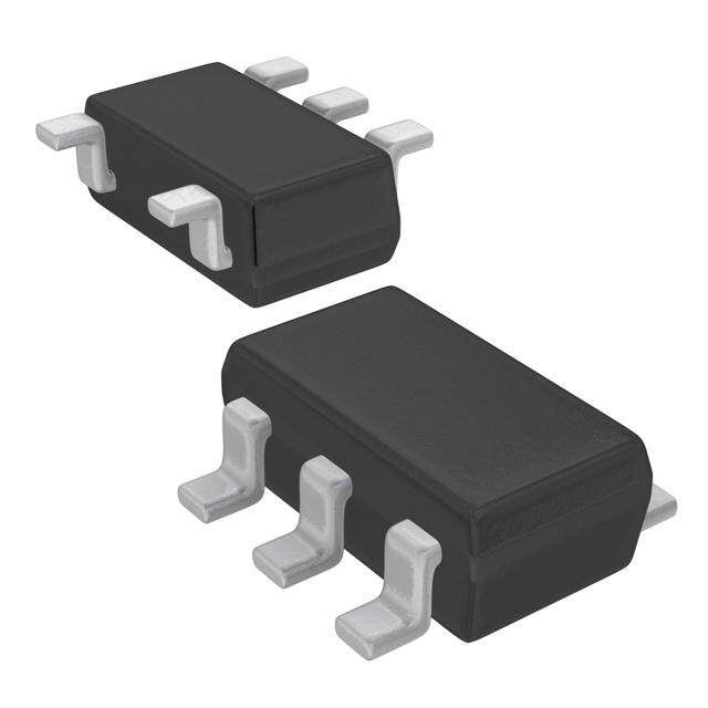
| 描述 | IC MXR 400MHZ-2.5GHZ DWN SOT23-6上下转换器 400MHz to 2.5GHz Upconverter |
| 产品分类 | |
| 品牌 | Maxim Integrated |
| 产品手册 | |
| 产品图片 |
|
| rohs | 符合RoHS无铅 / 符合限制有害物质指令(RoHS)规范要求 |
| 产品系列 | RF集成电路,上下转换器,Maxim Integrated MAX2681EUT+T- |
| 数据手册 | |
| 产品型号 | MAX2681EUT+T |
| RF类型 | 手机,ISM,PCS,WLL |
| 产品培训模块 | http://www.digikey.cn/PTM/IndividualPTM.page?site=cn&lang=zhs&ptm=25703http://www.digikey.cn/PTM/IndividualPTM.page?site=cn&lang=zhs&ptm=25705 |
| 产品种类 | 上下转换器 |
| 供应商器件封装 | SOT-23-6 |
| 其它名称 | MAX2681EUT+TDKR |
| 功率增益 | 14.2 dB |
| 包装 | Digi-Reel® |
| 商标 | Maxim Integrated |
| 噪声系数 | 12.7dB |
| 增益 | 14.2dB |
| 安装风格 | SMD/SMT |
| 封装 | Reel |
| 封装/外壳 | SOT-23-6 |
| 封装/箱体 | SOT-23-6 |
| 工作电源电压 | 3.3 V, 5 V |
| 工厂包装数量 | 2500 |
| 应用说明 | 点击此处下载产品Datasheet点击此处下载产品Datasheet点击此处下载产品Datasheet点击此处下载产品Datasheet |
| 最大功率耗散 | 696 mW |
| 最大工作温度 | + 85 C |
| 最小工作温度 | - 40 C |
| 标准包装 | 1 |
| 混频器数 | 1 |
| 电压-电源 | 2.7 V ~ 5.5 V |
| 电流-电源 | 8.7mA |
| 系列 | MAX2681 |
| 辅助属性 | 降频变频器 |
| 零件号别名 | MAX2681 |
| 频率 | 400MHz ~ 2.5GHz |


- 商务部:美国ITC正式对集成电路等产品启动337调查
- 曝三星4nm工艺存在良率问题 高通将骁龙8 Gen1或转产台积电
- 太阳诱电将投资9.5亿元在常州建新厂生产MLCC 预计2023年完工
- 英特尔发布欧洲新工厂建设计划 深化IDM 2.0 战略
- 台积电先进制程称霸业界 有大客户加持明年业绩稳了
- 达到5530亿美元!SIA预计今年全球半导体销售额将创下新高
- 英特尔拟将自动驾驶子公司Mobileye上市 估值或超500亿美元
- 三星加码芯片和SET,合并消费电子和移动部门,撤换高东真等 CEO
- 三星电子宣布重大人事变动 还合并消费电子和移动部门
- 海关总署:前11个月进口集成电路产品价值2.52万亿元 增长14.8%


PDF Datasheet 数据手册内容提取
EVALUATION KIT AVAILABLE MAX2680/MAX2681/ 400MHz to 2.5GHz, Low-Noise, MAX2682 SiGe Downconverter Mixers General Description Features The MAX2680/MAX2681/MAX2682 miniature, low-cost, ● 400MHz to 2.5GHz Operation low-noise downconverter mixers are designed for low- ● +2.7V to +5.5V Single-Supply Operation voltage operation and are ideal for use in portable com- ● Low Noise Figure: 6.3dB at 900MHz (MAX2680) munications equipment. Signals at the RF input port are mixed with signals at the local oscillator (LO) port using ● High Input Third-Order Intercept Point a double-balanced mixer. These downconverter mixers (IIP3 at 2450MHz) operate with RF input frequencies between 400MHz and • -6.9dBm at 5.0mA (MAX2680) 2500MHz, and downconvert to IF output frequencies • +1.0dBm at 8.7mA (MAX2681) between 10MHz and 500MHz. • +3.2dBm at 15.0mA (MAX2682) The MAX2680/MAX2681/MAX2682 operate from a single ● < 0.1μA Low-Power Shutdown Mode +2.7V to +5.5V supply, allowing them to be powered ● Ultra-Small Surface-Mount Packaging directly from a 3-cell NiCd or a 1-cell Lithium battery. These devices offer a wide range of supply currents and input intercept (IIP3) levels to optimize system perfor- mance. Additionally, each device features a low-power shutdown mode in which it typically draws less than 0.1μA of supply current. Consult the Selector Guide for various combinations of IIP3 and supply current. The MAX2680/MAX2681/MAX2682 are manufactured on a high-frequency, low-noise, advanced silicon-germanium process and are offered in the space-saving 6-pin SOT23 package. Ordering Information Applications PIN- SOT ● 400MHz/900MHz/2.4GHz ISM-Band Radios PART TEMP RANGE PACKAGE TOP MARK ● Personal Communications Systems (PCS) ● Cellular and Cordless Phones MAX2680EUT-T -40°C to +85°C 6 SOT23 AAAR ● Wireless Local Loop MAX2681EUT-T -40°C to +85°C 6 SOT23 AAAS ● IEEE-802.11 and Wireless Data MAX2682EUT-T -40°C to +85°C 6 SOT23 AAAT Selector Guide FREQUENCY PART ICC 900MHz 1950MHz 2450MHz (mA) IIP3 NF GAIN IIP3 NF GAIN IIP3 NF GAIN (dBm) (dB) (dB) (dBm) (dB) (dB) (dBm) (dB) (dB) MAX2680 5.0 -12.9 6.3 11.6 -8.2 8.3 7.6 -6.9 11.7 7.0 MAX2681 8.7 -6.1 7.0 14.2 +0.5 11.1 8.4 +1.0 12.7 7.7 MAX2682 15.0 -1.8 6.5 14.7 +4.4 10.2 10.4 +3.2 13.4 7.9 Typical Operating Circuit appears at end of data sheet. 19-4786; Rev 2; 8/03
MAX2680/MAX2681/ 400MHz to 2.5GHz, Low-Noise, MAX2682 SiGe Downconverter Mixers Absolute Maximum Ratings VCC to GND .........................................................-0.3V to +6.0V Continuous Power Dissipation (TA = +70°C) RFIN Input Power (50Ω source) .....................................+10dBm SOT23 (derate 8.7mW/°C above +70°C) ....................696mW LO Input Power (50Ω source) ........................................+10dBm Operating Temperature Range ...........................-40°C to +85°C SHDN, IFOUT, RFIN to GND ...................-0.3V to (VCC + 0.3V) Junction Temperature ......................................................+150°C LO to GND.......................................(VCC - 1V) to (VCC + 0.3V) Storage Temperature Range ............................-65°C to +160°C Lead Temperature (soldering, 10s) .................................+300°C Stresses beyond those listed under “Absolute Maximum Ratings” may cause permanent damage to the device. These are stress ratings only, and functional operation of the device at these or any other conditions beyond those indicated in the operational sections of the specifications is not implied. Exposure to absolute maximum rating conditions for extended periods may affect device reliability. CAUTION! ESD SENSITIVE DEVICE DC Electrical Characteristics (VCC = +2.7V to +5.5V, SHDN = +2V, TA = TMIN to TMAX unless otherwise noted. Typical values are at VCC = +3V and TA = +25°C. Minimum and maximum values are guaranteed over temperature by design and characterization.) PARAMETER SYMBOL CONDITIONS MIN TYP MAX UNITS MAX2680 5.0 7.7 Operating Supply Current ICC MAX2681 8.7 12.7 mA MAX2682 15.0 21.8 Shutdown Supply Current ICC SHDN = 0.5V 0.05 μA Shutdown Input Voltage High VIH 2.0 V Shutdown Input Voltage Low VIL 0.5 V Shutdown Input Bias Current ISHDN 0 < SHDN < VCC 0.2 μA AC Electrical Characteristics (MAX2680/1/2 EV Kit, VCC = SHDN = +3.0V, TA = +25°C, unless otherwise noted. RFIN and IFOUT matched to 50Ω. PLO = -5dBm, PRFIN = -25dBm.) PARAMETER CONDITIONS MIN TYP MAX UNITS MAX2680 RF Frequency Range (Notes 1, 2) 400 2500 MHz LO Frequency Range (Notes 1, 2) 400 2500 MHz IF Frequency Range (Notes 1, 2) 10 500 MHz fRF = 400MHz, fLO = 445MHz, fIF = 45MHz 7.3 fRF = 900MHz, fLO = 970MHz, fIF = 70MHz 11.6 Conversion Power Gain dB fRF = 1950MHz, fLO = 1880MHz, fIF = 70MHz (Note 1) 5.7 7.6 8.6 fRF = 2450MHz, fLO = 2210MHz, fIF = 240MHz 7.0 Gain Variation Over Temperature fRF = 1950MHz, fLO = 1880MHz, fIF = 70MHz, 1.9 2.4 dB TA = TMIN to TMAX (Note 1) fRF = 900MHz, 901MHz, fLO = 970MHz, fIF = 70MHz -12.9 Input Third-Order Intercept Point (Note 3) fRF = 1950MHz, 1951MHz, fLO = 1880MHz, fIF = 70MHz -8.2 dBm fRF = 2450MHz, 2451MHz, fLO = 2210MHz, fIF = 240MHz -6.9 fRF = 900MHz, fLO = 970MHz, fIF = 70MHz 6.3 Noise Figure (Single Sideband) fRF = 1950MHz, fLO = 2020MHz, fIF = 70MHz 8.3 dB fRF = 2450MHz, fLO = 2210MHz, fIF = 240MHz 11.7 LO Input VSWR 50Ω source impedance 1.5:1 LO Leakage at IFOUT Port fLO = 1880MHz -22 dBm www.maximintegrated.com Maxim Integrated │ 2
MAX2680/MAX2681/ 400MHz to 2.5GHz, Low-Noise, MAX2682 SiGe Downconverter Mixers AC Electrical Characteristics (continued) (MAX2680/1/2 EV Kit, VCC = SHDN = +3.0V, TA = +25°C, unless otherwise noted. RFIN and IFOUT matched to 50Ω. PLO = -5dBm, PRFIN = -25dBm.) PARAMETER CONDITIONS MIN TYP MAX UNITS LO Leakage at RFIN Port fLO = 1880MHz -26 dBm IF/2 Spurious Response fRF = 1915MHz, fLO = 1880MHz, fIF = 70MHz (Note 4) -51 dBm MAX2681 RF Frequency Range (Notes 1, 2) 400 2500 MHz LO Frequency Range (Notes 1, 2) 400 2500 MHz IF Frequency Range (Notes 1, 2) 10 500 MHz fRF = 400MHz, fLO = 445MHz, fIF = 45MHz 11.0 fRF = 900MHz, fLO = 970MHz, fIF = 70MHz 14.2 Conversion Power Gain dB fRF = 1950MHz, fLO = 1880MHz, fIF = 70MHz (Note 1) 6.7 8.4 9.4 fRF = 2450MHz, fLO = 2210MHz, fIF = 240MHz 7.7 Gain Variation Over Temperature fRF = 1950MHz, fLO = 1880MHz, fIF = 70MHz, 1.7 2.3 dB TA = TMIN to TMAX (Note 1) fRF = 900MHz, 901MHz, fLO = 970MHz, fIF = 70MHz -6.1 Input Third-Order Intercept Point (Note 3) fRF = 1950MHz, 1951MHz, fLO = 1880MHz, fIF = 70MHz +0.5 dBm fRF = 2450MHz, 2451MHz, fLO = 2210MHz, fIF = 240MHz +1.0 fRF = 900MHz, fLO = 970MHz, fIF = 70MHz 7.0 Noise Figure (Single Sideband) fRF = 1950MHz, fLO = 2020MHz, fIF = 70MHz 11.1 dB fRF = 2450MHz, fLO = 2210MHz, fIF = 240MHz 12.7 LO Input VSWR 50Ω source impedance 1.5:1 LO Leakage at IFOUT Port fLO = 1880MHz -23 dBm LO Leakage at RFIN Port fLO = 1880MHz -27 dBm IF/2 Spurious Response fRF = 1915MHz, fLO = 1880MHz, fIF = 70MHz (Note 4) -65 dBm MAX2682 RF Frequency Range (Notes 1, 2) 400 2500 MHz LO Frequency Range (Notes 1, 2) 400 2500 MHz IF Frequency Range (Notes 1, 2) 10 500 MHz fRF = 400MHz, fLO = 445MHz, fIF = 45MHz 13.4 fRF = 900MHz, fLO = 970MHz, fIF = 70MHz 14.7 Conversion Power Gain dB fRF = 1950MHz, fLO = 1880MHz, fIF = 70MHz (Note 1) 8.7 10.4 11.7 fRF = 2450MHz, fLO = 2210MHz, fIF = 240MHz 7.9 Gain Variation Over Temperature fRF = 1950MHz, fLO = 1880MHz, fIF = 70MHz, 2.1 3.2 dB TA = TMIN to TMAX (Note 1) fRF = 900MHz, 901MHz, fLO = 970MHz, fIF = 70MHz -1.8 Input Third-Order Intercept Point (Note 3) fRF = 1950MHz, 1951MHz, fLO = 1880MHz, fIF = 70MHz +4.4 dBm fRF = 2450MHz, 2451MHz, fLO = 2210MHz, fIF = 240MHz +3.2 fRF = 900MHz, fLO = 970MHz, fIF = 70MHz 6.5 Noise Figure (Single Sideband) fRF = 1950MHz, fLO = 2020MHz, fIF = 70MHz 10.2 dB fRF = 2450MHz, fLO = 2210MHz, fIF = 240MHz 13.4 www.maximintegrated.com Maxim Integrated │ 3
MAX2680/MAX2681/ 400MHz to 2.5GHz, Low-Noise, MAX2682 SiGe Downconverter Mixers AC Electrical Characteristics (continued) (MAX2680/1/2 EV Kit, VCC = SHDN = +3.0V, TA = +25°C, unless otherwise noted. RFIN and IFOUT matched to 50Ω. PLO = -5dBm, PRFIN = -25dBm.) PARAMETER CONDITIONS MIN TYP MAX UNITS LO Input VSWR 50Ω source impedance 1.5:1 LO Leakage at IFOUT Port fLO = 1880MHz -23 dBm LO Leakage at RFIN Port fLO = 1880MHz -27 dBm IF/2 Spurious Response fRF = 1915MHz, fLO = 1880MHz, fIF = 70MHz (Note 4) -61 dBm Note 1: Guaranteed by design and characterization. Note 2: Operation outside of this specification is possible, but performance is not characterized and is not guaranteed. Note 3: Two input tones at -25dBm per tone. Note 4: This spurious response is caused by a higher-order mixing product (2x2). Specified RF frequency is applied and IF output power is observed at the desired IF frequency (70MHz). Typical Operating Characteristics (Typical Operating Circuit, VCC = SHDN = +3.0V, PRFIN = -25dBm, PLO = -5dBm, TA = +25°C, unless otherwise noted.) MAX2680 MAX2681 MAX2682 SUPPLY CURRENT vs. SUPPLY VOLTAGE SUPPLY CURRENT vs. SUPPLY VOLTAGE SUPPLY CURRENT vs. SUPPLY VOLTAGE 67 SHDN = VCC MAX2680/1/2-01 190 SHDN = VCC TA = +85°C MAX2680/1/2-02 111678 TA = +85°C SHDN = VCC MAX2680/1/2-03 T (mA) TA = +85°C TA = +25°C T (mA) T (mA) 15 EN 5 EN 8 EN 14 R R R CUR CUR TA = +25°C CUR 13 TA = +25°C TA = -40°C LY 4 LY 7 TA = -40°C LY 12 PP TA = -40°C PP PP U U U 11 S S S 3 6 10 9 2 5 8 2.5 3.0 3.5 4.0 4.5 5.0 5.5 2.5 3.0 3.5 4.0 4.5 5.0 5.5 2.5 3.0 3.5 4.0 4.5 5.0 5.5 SUPPLY VOLTAGE (V) SUPPLY VOLTAGE (V) SUPPLY VOLTAGE (V) www.maximintegrated.com Maxim Integrated │ 4
MAX2680/MAX2681/ 400MHz to 2.5GHz, Low-Noise, MAX2682 SiGe Downconverter Mixers Typical Operating Characteristics (continued) (Typical Operating Circuit, VCC = SHDN = +3.0V, PRFIN = -25dBm, PLO = -5dBm, TA = +25°C, unless otherwise noted.) MAX2680 MAX2681 MAX2682 SHUTDOWN SUPPLY SHUTDOWN SUPPLY SHUTDOWN SUPPLY CURRENT vs. SUPPLY VOLTAGE CURRENT vs. SUPPLY VOLTAGE CURRENT vs. SUPPLY VOLTAGE 0.10 0.10 0.10 NT (µA)00..0089 SHDN = GND MAX2680/1/2-04 NT (µA)00..0089 SHDN = GND MAX2680/1/2-05 NT (µA)00..0089 SHDN = GND MAX2680/1/2-06 E E E R0.07 R0.07 R0.07 CUR0.06 TA = +25°C TA = +85°C CUR0.06 TA = +25°C TA = +85°C CUR0.06 TA = +25°C TA = +85°C Y Y Y PL0.05 PL0.05 PL0.05 P P P U U U S0.04 S0.04 S0.04 N N N DOW0.03 TA = -40°C DOW0.03 TA = -40°C DOW0.03 TA = -40°C UT0.02 UT0.02 UT0.02 H H H S S S 0.01 0.01 0.01 0 0 0 2.5 3.0 3.5 4.0 4.5 5.0 5.5 2.5 3.0 3.5 4.0 4.5 5.0 5.5 2.5 3.0 3.5 4.0 4.5 5.0 5.5 SUPPLY VOLTAGE (V) SUPPLY VOLTAGE (V) SUPPLY VOLTAGE (V) MAX2680 MAX2681 MAX2682 CONVERSION POWER GAIN vs. LO POWER CONVERSION POWER GAIN vs. LO POWER CONVERSION POWER GAIN vs. LO POWER 15 16 16 GAIN (dB) 1113 fRF = 900MHz fRF = 1950MHz MAX2680/1/2-07 GAIN (dB) 1124 fRF = 900MHz MAX2680/1/2-08 GAIN (dB) 1124 fRF = 900MHz fRF = 1950MHz MAX2680/1/2-09 ER 9 fRF = 2450MHz ER 10 fRF = 1950MHz ER 10 W W W O O O P 7 P 8 P 8 SION 5 SION 6 fRF = 2450MHz SION 6 fRF = 2450MHz R R R E E E NV 3 fRF fLO fIF NV 4 fRF fLO fIF NV 4 fRF fLO fIF CO 900MHz 970MHz 70MHz CO 900MHz 970MHz 70MHz CO 900MHz 970MHz 70MHz 1 1950MHz1880MHz70MHz 2 1950MHz1880MHz70MHz 2 1950MHz1880MHz70MHz 2450MHz2210MHz240MHz 2450MHz2210MHz240MHz 2450MHz2210MHz240MHz -1 0 0 -14 -12 -10 -8 -6 -4 -2 0 -14 -12 -10 -8 -6 -4 -2 0 -14 -12 -10 -8 -6 -4 -2 0 LO POWER (dBm) LO POWER (dBm) LO POWER (dBm) MAX2680 MAX2681 MAX2682 CONVERSION POWER GAIN vs. TEMPERATURE CONVERSION POWER GAIN vs. TEMPERATURE CONVERSION POWER GAIN vs. TEMPERATURE 16 16 17 AIN (dB) 1124 fRF = 900MHz MAX2680/1/2-10 AIN (dB) 1124 fRF = 900MHz MAX2680/1/2-11 AIN (dB) 1135 fRF = 900MHz MAX2680/1/2-12 G G G WER 10 WER 10 fRF = 1950MHz WER 11 fRF = 1950MHz PO 8 fRF = 1950MHz PO 8 PO 9 N N N RSIO 6 fRF = 2450MHz RSIO 6 fRF = 2450MHz RSIO 7 fRF = 2450MHz E E E NV 4 fRF fLO fIF NV 4 NV 5 CO 900MHz 970MHz 70MHz CO CO 2 1950MHz1880MHz 70MHz 2 3 2450MHz2210MHz240MHz 0 0 1 -40 -20 0 20 40 60 80 100 -40 -20 0 20 40 60 80 100 -40 -20 0 20 40 60 80 100 TEMPERATURE (°C) TEMPERATURE (°C) TEMPERATURE (°C) www.maximintegrated.com Maxim Integrated │ 5
MAX2680/MAX2681/ 400MHz to 2.5GHz, Low-Noise, MAX2682 SiGe Downconverter Mixers Typical Operating Characteristics (continued) (Typical Operating Circuit, VCC = SHDN = +3.0V, PRFIN = -25dBm, PLO = -5dBm, TA = +25°C, unless otherwise noted.) MAX2680 MAX2681 MAX2682 INPUT IP3 vs. LO POWER INPUT IP3 vs. LO POWER INPUT IP3 vs. LO POWER -5 2 7 -6 fffRLIFOF = = =7 1 019M858H00MzMHHzz, 1951MHz MAX2680/1/2-13 1 MAX2680/1/2-14 6 fffRLIFOF = = =7 1 019M858H00MzMHHzz, 1951MHz MAX2680/1/2-15 PRFIN = -25dBm PER TONE 5 PRFIN = -25dBm PER TONE m) m) m) B B B 3 (d -7 3 (d 0 3 (d 4 P P P T I T I T I U U U 3 P -8 P -1 P N N N I I I fRF = 1950MHz, 1951MHz 2 -9 -2 fLO = 1880MHz fIF = 70MHz 1 PRFIN = -25dBm PER TONE -10 -3 0 -14 -12 -10 -8 -6 -4 -2 0 -14 -12 -10 -8 -6 -4 -2 0 -14 -12 -10 -8 -6 -4 -2 0 LO POWER (dBm) LO POWER (dBm) LO POWER (dBm) MAX2680 MAX2681 MAX2682 NOISE FIGURE vs. LO POWER NOISE FIGURE vs. LO POWER NOISE FIGURE vs. LO POWER 16 20 25 14 fRF = 2450MHz MAX2680/1/2-16 1168 MAX2680/1/2-17 20 199050f0RMMFHHzz290720f0LMOMHHzz7700fMMIFHHzz MAX2680/1/2-18 B) 12 B) 14 fRF = 2450MHz B) 2450MHz2210MHz70MHz d d d URE ( 10 fRF = 1950MHz URE ( 12 fRF = 1950MHz URE ( 15 fRF = 2450MHz FIG 8 FIG 10 FIG OISE 6 fRF = 900MHz OISE 8 fRF = 900MHz OISE 10 fRF = 1950MHz N 4 fRF fLO fIF N 6 fRF fLO fIF N fRF = 900MHz 900MHz 970MHz 70MHz 4 900MHz 970MHz 70MHz 5 2 1950MHz2020MHz70MHz 2 1950MHz2020MHz70MHz 2450MHz2210MHz70MHz 2450MHz2210MHz70MHz 0 0 0 -14 -12 -10 -8 -6 -4 -2 0 -14 -12 -10 -8 -6 -4 -2 0 -14 -12 -10 -8 -6 -4 -2 0 LO POWER (dBm) LO POWER (dBm) LO POWER (dBm) MAX2680 MAX2681 MAX2682 RF PORT IMPEDANCE vs. RF FREQUENCY RF PORT IMPEDANCE vs. RF FREQUENCY RF PORT IMPEDANCE vs. RF FREQUENCY 300 MAX2680/1/2-19 0 300 MAX2680/1/2-20 0 300 MAX2680/1/2-21 0 IMAGINARY 250 -100 W) 250 IMAGINARY -100 Ω) 250 IMAGINARY -100 Ω) Ω) E ( Ω) E ( Ω) E ( E (200 -200 NC E (200 -200 NC E (200 -200 NC C A C A C A N D N D N D A E A E A E D P D P D P E150 -300 M E150 -300 M E150 -300 M MP Y I MP Y I MP Y I L I AR L I AR L I AR REA100 -400 AGIN REA100 -400 AGIN REA100 -400 AGIN M M M 50 PfLLOO = = 9 -750dMBmHz REAL -500 I 50 PfLLOO = = 9 -750dMBmHz REAL -500 I 50 PfLLOO = = 9 -750dMBmHz REAL -500 I 0 -600 0 -600 0 -600 0 500 1000 1500 2000 2500 0 500 1000 1500 2000 2500 0 500 1000 1500 2000 2500 RF FREQUENCY (MHz) RF FREQUENCY (MHz) RF FREQUENCY (MHz) www.maximintegrated.com Maxim Integrated │ 6
MAX2680/MAX2681/ 400MHz to 2.5GHz, Low-Noise, MAX2682 SiGe Downconverter Mixers Typical Operating Characteristics (continued) (Typical Operating Circuit, VCC = SHDN = +3.0V, PRFIN = -25dBm, PLO = -5dBm, TA = +25°C, unless otherwise noted.) MAX2680 MAX2681 MAX2682 IF PORT IMPEDANCE vs. IF FREQUENCY IF PORT IMPEDANCE vs. IF FREQUENCY IF PORT IMPEDANCE vs. IF FREQUENCY 1200 MAX2680/1/2-22 0 1200 MAX2680/1/2-23 0 800 MAX2680/1/2-24 0 fLO = 970MHz fLO = 970MHz fLO = 970MHz PLO = -5dBm PLO = -5dBm 700 PLO = -5dBm -50 1000 -100 Ω) 1000 -100 Ω) Ω) Ω) E ( Ω) E ( Ω)600 -100 E ( ANCE (800 IMAGINARY -200 EDANC ANCE (800 IMAGINARY -200 EDANC ANCE (500 IMAGINARY -150 EDANC D P D P D P E600 -300 M E600 -300 M E400 -200 M MP Y I MP Y I MP Y I L I AR L I AR L I300 -250 AR REA400 -400 MAGIN REA400 -400 MAGIN REA200 -300 MAGIN I I I 200 REAL -500 200 REAL -500 100 REAL -350 0 -600 0 -600 0 -400 0 100 200 300 400 500 0 100 200 300 400 500 0 100 200 300 400 500 IF FREQUENCY (MHz) IF FREQUENCY (MHz) IF FREQUENCY (MHz) MAX2680 MAX2681 MAX2682 LO PORT RETURN LOSS LO PORT RETURN LOSS LO PORT RETURN LOSS +10 +10 +10 +50 MAX2680/1/2-25 +50 MAX2680/1/2-26 +50 MAX2680/1/2-27 B) -5 B) -5 B) -5 d d d S ( -10 S ( -10 S ( -10 S S S O O O N L -15 N L -15 N L -15 R R R U -20 U -20 U -20 T T T E E E R -25 R -25 R -25 -30 -30 -30 -35 -35 -35 -40 -40 -40 200 760 1320 1880 2440 3000 200 760 1320 1880 2440 3000 200 760 1320 1880 2440 3000 FREQUENCY (MHz) FREQUENCY (MHz) FREQUENCY (MHz) MAX2680 MAX2681 MAX2682 LO-to-IF AND LO-to-RF ISOLATION LO-to-IF AND LO-to-RF ISOLATION LO-to-IF AND LO-to-RF ISOLATION 3305 LO-to-IF ISOLATION MAX2680/1/2-28 4305 LO-to-IF ISOLATION MAX2680/1/2-29 3350 LO-to-IF ISOLATION MAX2680/1/2-30 30 25 B) B) B) ON (d 20 LO-to-RF ISOLATION ON (d 25 ON (d 25 TI TI 20 LO-to-RF ISOLATION TI A A A SOL 15 SOL 15 SOL 20 LO-to-RF ISOLATION I I I 10 10 15 5 5 0 0 10 0 500 1000 1500 2000 2500 0 500 1000 1500 2000 2500 0 500 1000 1500 2000 2500 LO FREQUENCY (MHz) LO FREQUENCY (MHz) LO FREQUENCY (MHz) www.maximintegrated.com Maxim Integrated │ 7
MAX2680/MAX2681/ 400MHz to 2.5GHz, Low-Noise, MAX2682 SiGe Downconverter Mixers Typical Operating Characteristics (continued) (Typical Operating Circuit, VCC = SHDN = +3.0V, PRFIN = -25dBm, PLO = -5dBm, TA = +25°C, unless otherwise noted.) MAX2680 MAX2681 MAX2682 TURN-OFF/ON CHARACTERISTICS TURN-OFF/ON CHARACTERISTICS TURN-OFF/ON CHARACTERISTICS S2VH/DdiNv MAX2680/1/2-31 S2VH/DdiNv MAX2680/1/2-32 S2VH/DdiNv MAX2680/1/2-33 IFOUT IFOUT IFOUT 50mV/ 50mV/ 50mV/ div div div Z1 = 39pF Z1 = 39pF Z2 = 39pF 500ns/div 500ns/div 500ns/div Pin Configuration TOP VIEW LO 1 6 SHDN MAX2680 MAX2681 GND 2 MAX2682 5 VCC RFIN 3 4 IFOUT SOT23-6 Pin Description PIN NAME FUNCTION Local-Oscillator Input. Apply a local-oscillator signal with an amplitude of -10dBm to 0 (50Ω source). 1 LO AC-couple this pin to the oscillator with a DC-blocking capacitor. Nominal DC voltage is VCC - 0.4V. 2 GND Mixer Ground. Connect to the ground plane with a low-inductance connection. Radio Frequency Input. AC-couple to this pin with a DC-blocking capacitor. Nominal DC voltage is 1.5V. 3 RFIN See the Applications Information section for details on impedance matching. 4 IFOUT Intermediate Frequency Output. Open-collector output requires an inductor to VCC. AC-couple to this pin with a DC-blocking capacitor. See the Applications Information section for details on impedance matching. Supply Voltage Input, +2.7V to +5.5V. Bypass with a capacitor to the ground plane. Capacitor value depends 5 VCC upon desired operating frequency. Active-Low Shutdown. Drive low to disable all device functions and reduce the supply current to less than 6 SHDN 5μA. For normal operation, drive high or connect to VCC. www.maximintegrated.com Maxim Integrated │ 8
MAX2680/MAX2681/ 400MHz to 2.5GHz, Low-Noise, MAX2682 SiGe Downconverter Mixers Detailed Description IF Output The MAX2680/MAX2681/MAX2682 are 400MHz to The IF output frequency range extends from 10MHz to 2.5GHz, silicon-germanium, double-balanced downcon- 500MHz. IFOUT is a high-impedance, open-collector output verter mixers. They are designed to provide optimum that requires an external inductor to VCC for proper biasing. linearity performance for a specified supply current. For optimum performance, the IF port requires an imped- They consist of a double-balanced Gilbert-cell mixer with ance-matching network. The configuration and values for single-ended RF, LO, and IF port connections. An on-chip the matching network is dependent upon the frequency and bias cell provides a low-power shutdown feature. Consult desired output impedance. For assistance in choosing com- the Selector Guide for device features and comparison. ponents for optimal performance, see Table 3 and Table 4 as well as the IF Port Impedance vs. IF Frequency graph in Applications Information the Typical Operating Characteristics section. Local-Oscillator (LO) Input Power-Supply and SHDN Bypassing The LO input is a single-ended broadband port with a Proper attention to voltage supply bypassing is essential typical input VSWR of better than 2.0:1 from 400MHz to for high-frequency RF circuit stability. Bypass VCC with a 2.5GHz. The LO signal is mixed with the RF input sig- 10μF capacitor in parallel with a 1000pF capacitor. Use nal, and the resulting downconverted output appears at separate vias to the ground plane for each of the bypass IFOUT. AC-couple LO with a capacitor. Drive the LO port capacitors and minimize trace length to reduce induc- with a signal ranging from -10dBm to 0 (50Ω source). tance. Use separate vias to the ground plane for each ground pin. Use low-inductance ground connections. RF Input Decouple SHDN with a 1000pF capacitor to ground to The RF input frequency range is 400MHz to 2.5GHz. minimize noise on the internal bias cell. Use a series The RF input requires an impedance-matching network resistor (typically 100Ω) to reduce coupling of high-fre- as well as a DC-blocking capacitor that can be part of quency signals into the SHDN pin. the matching network. Consult Tables 1 and 2, as well as the RF Port Impedance vs. RF Frequency graph in the Layout Issues Typical Operating Characteristics section for information A well-designed PC board is an essential part of an RF on matching. circuit. For best performance, pay attention to power- supply issues as well as to the layout of the RFIN and IFOUT impedance-matching network. Table 1. RFIN Port Impedance FREQUENCY PART 400MHz 900MHz 1950MHz 2450MHz MAX2680 179-j356 54-j179 32-j94 33-j73 MAX2681 209-j332 75-j188 34-j108 33-j86 MAX2682 206-j306 78-j182 34-j106 29-j86 Table 2. RF Input Impedance-Matching Component Values FREQUENCY MATCHING MAX2680 MAX2681 MAX2682 COMPONENTS 400 900 1950 2450 400 900 1950 2450 400 900 1950 2450 MHz MHz MHz MHz MHz MHz MHz MHz MHz MHz MHz MHz Z1 86nH 270pF 1.5pF Short 68nH 270pF 1.5pF Short 68nH 1.5pF Short Short Z2 270pF 22nH 270pF 270pF 270pF 18nH 270pF 270pF 270pF 270pF 270pF 270pF Z3 Open Open 1.8nH 1.8nH 0.5pF Open 1.8nH 2.2nH 0.5pF 10nH 2.2nH 1.2nH Note: Z1, Z2, and Z3 are found in the Typical Operating Circuit. www.maximintegrated.com Maxim Integrated │ 9
MAX2680/MAX2681/ 400MHz to 2.5GHz, Low-Noise, MAX2682 SiGe Downconverter Mixers Table 3. IFOUT Port Impedance Power-Supply Layout To minimize coupling between different sections of the IC, FREQUENCY PART the ideal power-supply layout is a star configuration with 45MHz 70MHz 240MHz a large decoupling capacitor at a central VCC node. The MAX2680 960-j372 803-j785 186-j397 VCC traces branch out from this central node, each going MAX2681 934-j373 746-j526 161-j375 to a separate VCC node on the PC board. At the end of each trace is a bypass capacitor that has low ESR at the MAX2682 670-j216 578-j299 175-j296 RF frequency of operation. This arrangement provides local decoupling at the VCC pin. At high frequencies, any signal leaking out of one supply pin sees a relatively high Table 4. IF Output Impedance-Matching impedance (formed by the VCC trace inductance) to the Components central VCC node, and an even higher impedance to any other supply pin, as well as a low impedance to ground MATCHING FREQUENCY through the bypass capacitor. COMPONENT 45MHz 70MHz 240MHz Impedance-Matching Network Layout L1 390nH 330nH 82nH The RFIN and IFOUT impedance-matching networks C2 39pF 15pF 3pF are very sensitive to layout-related parasitics. To mini- R1 250Ω Open Open mize parasitic inductance, keep all traces short and place components as close as possible to the chip. To minimize parasitic capacitance, use cutouts in the ground plane (and any other plane) below the matching network components. However, avoid cutouts that are larger than necessary since they act as aperture antennas. Typical Operating Circuit C1 LO 1 6 SHUTDOWN LO SHDN INPUT CONTROL C3 MAX2680 MAX2681 MAX2682 2 GND VCC 5 VCC +2.7V TO +5.5V C4 C5 1000pF 10µF L1 R1 RF Z1 Z2 3 4 IF INPUT RFIN IFOUT OUTPUT C2 Z3 THE VALUES OF MATCHING COMPONENTS C2, L1, R1, Z1, Z2, AND Z3 DEPEND ON THE IF AND RF FREQUENCY AND DOWNCONVERTER. SEE TABLES 2 AND 4. www.maximintegrated.com Maxim Integrated │ 10
MAX2680/MAX2681/ 400MHz to 2.5GHz, Low-Noise, MAX2682 SiGe Downconverter Mixers Package Information For the latest package outline information and land patterns (footprints), go to www.maximintegrated.com/packages. Note that a “+”, “#”, or “-” in the package code indicates RoHS status only. Package drawings may show a different suffix character, but the drawing pertains to the package regardless of RoHS status. www.maximintegrated.com Maxim Integrated │ 11
MAX2680/MAX2681/ 400MHz to 2.5GHz, Low-Noise, MAX2682 SiGe Downconverter Mixers Package Information (continued) For the latest package outline information and land patterns (footprints), go to www.maximintegrated.com/packages. Note that a “+”, “#”, or “-” in the package code indicates RoHS status only. Package drawings may show a different suffix character, but the drawing pertains to the package regardless of RoHS status. For pricing, delivery, and ordering information, please contact Maxim Direct at 1-888-629-4642, or visit Maxim Integrated’s website at www.maximintegrated.com. Maxim Integrated cannot assume responsibility for use of any circuitry other than circuitry entirely embodied in a Maxim Integrated product. No circuit patent licenses are implied. Maxim Integrated reserves the right to change the circuitry and specifications without notice at any time. The parametric values (min and max limits) shown in the Electrical Characteristics table are guaranteed. Other parametric values quoted in this data sheet are provided for guidance. Maxim Integrated and the Maxim Integrated logo are trademarks of Maxim Integrated Products, Inc. © 2003 Maxim Integrated Products, Inc. │ 12
Mouser Electronics Authorized Distributor Click to View Pricing, Inventory, Delivery & Lifecycle Information: M axim Integrated: MAX2680EUT-T MAX2681EUT-T MAX2680AUT+T MAX2680EUT+T MAX2681EUT+T