ICGOO在线商城 > 集成电路(IC) > 接口 - 驱动器,接收器,收发器 > MAX208EENG+

 Datasheet下载
- 型号: MAX208EENG+
- 制造商: Maxim
- 库位|库存: xxxx|xxxx
- 要求:
| 数量阶梯 | 香港交货 | 国内含税 |
| +xxxx | $xxxx | ¥xxxx |
查看当月历史价格
查看今年历史价格
MAX208EENG+产品简介:
ICGOO电子元器件商城为您提供MAX208EENG+由Maxim设计生产,在icgoo商城现货销售,并且可以通过原厂、代理商等渠道进行代购。 MAX208EENG+价格参考¥60.52-¥60.52。MaximMAX208EENG+封装/规格:接口 - 驱动器,接收器,收发器, 完全版 收发器 4/4 RS232 24-PDIP。您可以下载MAX208EENG+参考资料、Datasheet数据手册功能说明书,资料中有MAX208EENG+ 详细功能的应用电路图电压和使用方法及教程。
MAX208EENG+是Maxim Integrated公司生产的一款RS-232收发器,属于接口类驱动器/接收器/收发器产品。该芯片集成了电荷泵电路,可由单电源(通常为+5V)供电,实现TTL/CMOS电平与RS-232电平之间的双向转换,适用于需要串行通信的工业和消费类电子设备。

其典型应用场景包括:工业控制系统的数据通信模块,用于连接微控制器与上位机或外围设备;嵌入式系统中的串口扩展接口,支持调试信息输出或设备配置;医疗设备中用于可靠的数据传输;测试测量仪器与计算机之间的通信接口;以及POS终端、安防设备和通信网关等需要稳定、低功耗串行通信的场合。

MAX208EENG+具有±15kV ESD保护、低功耗待机模式和内置电压倍增器,无需外部升压电路,简化了设计并提高了系统可靠性。其工作温度范围为-40°C至+85°C,符合工业级应用要求,适合在恶劣环境中长期稳定运行。此外,该器件采用28引脚PDIP封装,便于原型开发和手工焊接,广泛应用于对可靠性与兼容性要求较高的RS-232通信场景。
| 参数 | 数值 |
| 产品目录 | 集成电路 (IC)半导体 |
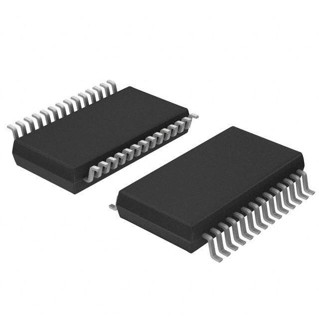
| 描述 | IC TXRX RS-232 W/CAP 24-DIPRS-232接口集成电路 15kV ESD-Protected 5V RS232 Transceiver |
| 产品分类 | |
| 品牌 | Maxim Integrated |
| 产品手册 | |
| 产品图片 |
|
| rohs | 符合RoHS无铅 / 符合限制有害物质指令(RoHS)规范要求 |
| 产品系列 | 接口 IC,RS-232接口集成电路,Maxim Integrated MAX208EENG+- |
| 数据手册 | |
| 产品型号 | MAX208EENG+ |
| 产品培训模块 | http://www.digikey.cn/PTM/IndividualPTM.page?site=cn&lang=zhs&ptm=25703http://www.digikey.cn/PTM/IndividualPTM.page?site=cn&lang=zhs&ptm=25705 |
| 产品目录页面 | |
| 产品种类 | RS-232接口集成电路 |
| 传播延迟时间ns | 10 us |
| 供应商器件封装 | 24-PDIP |
| 关闭 | No |
| 功能 | Transceiver |
| 包装 | 管件 |
| 协议 | RS232 |
| 双工 | 全 |
| 商标 | Maxim Integrated |
| 安装类型 | 通孔 |
| 安装风格 | Through Hole |
| 封装 | Tube |
| 封装/外壳 | 24-DIP(0.300",7.62mm) |
| 封装/箱体 | PDIP-Narrow-24 |
| 工作温度 | -40°C ~ 85°C |
| 工作温度范围 | - 40 C to + 85 C |
| 工作电源电压 | 5 V |
| 工厂包装数量 | 15 |
| 应用说明 | |
| 接收器滞后 | 500mV |
| 接收机数量 | 4 Receiver |
| 数据速率 | 120Kbps |
| 最大工作温度 | + 85 C |
| 最小工作温度 | - 40 C |
| 标准包装 | 1 |
| 激励器数量 | 4 Driver |
| 电压-电源 | 4.5 V ~ 5.5 V |
| 电源电流 | 20 mA |
| 类型 | 收发器 |
| 系列 | MAX208E |
| 输入/输出端数量 | 16 |
| 零件号别名 | MAX208E |
| 驱动器/接收器数 | 4/4 |


- 商务部:美国ITC正式对集成电路等产品启动337调查
- 曝三星4nm工艺存在良率问题 高通将骁龙8 Gen1或转产台积电
- 太阳诱电将投资9.5亿元在常州建新厂生产MLCC 预计2023年完工
- 英特尔发布欧洲新工厂建设计划 深化IDM 2.0 战略
- 台积电先进制程称霸业界 有大客户加持明年业绩稳了
- 达到5530亿美元!SIA预计今年全球半导体销售额将创下新高
- 英特尔拟将自动驾驶子公司Mobileye上市 估值或超500亿美元
- 三星加码芯片和SET,合并消费电子和移动部门,撤换高东真等 CEO
- 三星电子宣布重大人事变动 还合并消费电子和移动部门
- 海关总署:前11个月进口集成电路产品价值2.52万亿元 增长14.8%


PDF Datasheet 数据手册内容提取
EVALUATION KIT AVAILABLE MAX202E–MAX213E, ±15kV ESD-Protected, MAX232E/MAX241E 5V RS-232 Transceivers General Description Benefits and Features The MAX202E-MAX213E, MAX232E, and MAX241E are a • Saves Board Space family of RS-232 and V.28 transceivers with high ±15kV • Integrated High ±15kV HBM ESD Protection ESD HBM protection and integrated charge pump circuit- • Integrated Charge Pump Circuitry ry for single +5V supply operation. The various combina- tions of features are outlined in the Selector Guide.The Eliminates the Need for a Bipolar ±12V Supply drivers and receivers for all ten devices meet all EIA/TIA- Enables Single Supply Operation From +5V Supply 232E and CCITT V.28 specifications at data rates up to • Integrated 0.1µF Capacitors (MAX203E, MAX205E) 120kbps when loaded. • 24 pin SSOP Package Saves up to 40% Versus SO The MAX211E/MAX213E/MAX241E are available in 28- Package pin SO and SSOP packages. The MAX202E/MAX232E • Saves Power for Reduced Power Requirements come in 16-pin TSSOP, narrow SO, wide SO, and DIP packages. The MAX203E comes in a 20-pin DIP/SO • 1µA Shutdown Mode package, and needs no external charge-pump capaci- • 15µA Shutdown Mode for MAX213E tors. The MAX205E comes in a 24-pin wide DIP pack- age, and also eliminates external charge-pump Ordering Information capacitors. Applications PART TEMP RANGE PIN-PACKAGE MAX202ECPE 0°C to +70°C 16 Plastic DIP • Battery-Powered Equipment MAX202ECSE 0°C to +70°C 16 Narrow SO • Hand-Held Equipment Ordering Information continued at end of data sheet. • Portable Diagnostics Equipment Pin Configurations and Typical Operating Circuits appear at end of data sheet. AutoShutdown and UCSP are trademarks of Maxim Integrated Products, Inc. NO. OF RECEIVERS NO. OF RS-232 NO. OF RS-232 EXTERNAL LOW-POWER TTL TRI- PART ACTIVE IN DRIVERS RECEIVERS CAPACITORS SHUTDOWN STATE SHUTDOWN (µF) MAX202E 2 2 0 4 (0.1) No No MAX203E 2 2 0 None No No MAX205E 5 5 0 None Yes Yes MAX206E 4 3 0 4 (0.1) Yes Yes MAX207E 5 3 0 4 (0.1) No No MAX208E 4 4 0 4 (0.1) No No MAX211E 4 5 0 4 (0.1) Yes Yes MAX213E 4 5 2 4 (0.1) Yes Yes MAX232E 2 2 0 4 (1) No No MAX241E 4 5 0 4 (1) Yes Yes 19-0175; Rev 7; 1/15
MAX202E–MAX213E, ±15kV ESD-Protected, MAX232E/MAX241E 5V RS-232 Transceivers Absolute Maximum Ratings 20-Pin Plastic DIP (derate 11.11mW/°C above +70°C)...889mW VCC..........................................................................-0.3V to +6V 20-Pin SO (derate 10.00mW/°C above +70°C).............800mW V+................................................................(VCC- 0.3V) to +14V 24-Pin Narrow Plastic DIP V-............................................................................-14V to +0.3V (derate 13.33mW/°C above +70°C) ...............................1.07W Input Voltages 24-Pin Wide Plastic DIP T_IN............................................................-0.3V to (V+ + 0.3V) (derate 14.29mW/°C above +70°C)................................1.14W R_IN...................................................................................±30V 24-Pin SO (derate 11.76mW/°C above +70°C).............941mW Output Voltages 24-Pin SSOP (derate 8.00mW/°C above +70°C)..........640mW T_OUT.................................................(V- - 0.3V) to (V+ + 0.3V) 28-Pin SO (derate 12.50mW/°C above +70°C)....................1W R_OUT......................................................-0.3V to (VCC+ 0.3V) 28-Pin SSOP (derate 9.52mW/°C above +70°C)..........762mW Short-Circuit Duration, T_OUT....................................Continuous Operating Temperature Ranges Continuous Power Dissipation (TA= +70°C) MAX2_ _EC_ _.....................................................0°C to +70°C 16-Pin Plastic DIP (derate 10.53mW/°C above +70°C)....842mW MAX2_ _EE_ _...................................................-40°C to +85°C 16-Pin Narrow SO (derate 8.70mW/°C above +70°C).....696mW Storage Temperature Range.............................-65°C to +165°C 16-Pin Wide SO (derate 9.52mW/°C above +70°C)......762mW Lead Temperature (soldering, 10s).................................+300°C 16-Pin TSSOP (derate 9.4mW/°C above +70°C)...........755mW Stresses beyond those listed under “Absolute Maximum Ratings” may cause permanent damage to the device. These are stress ratings only, and functional operation of the device at these or any other conditions beyond those indicated in the operational sections of the specifications is not implied. Exposure to absolute maximum rating conditions for extended periods may affect device reliability. Electrical Characteristics (VCC = +5V ±10% for MAX202E/206E/208E/211E/213E/232E/241E; VCC = +5V ±5% for MAX203E/205E/207E; C1–C4 = 0.1µF for MAX202E/206E/207E/208E/211E/213E; C1–C4 = 1µF for MAX232E/241E; TA= TMINto TMAX; unless otherwise noted. Typical values are at TA= +25°C.) PARAMETER SYMBOL CONDITIONS MIN TYP MAX UNITS DC CHARACTERISTICS MAX202E/203E 8 15 MAX205E–208E 11 20 VCCSupply Current ICC No load, TA= +25°C MAX211E/213E 14 20 mA MAX232E 5 10 MAX241E 7 15 MAX205E/206E 1 10 Shutdown Supply Current TA= +25°C, Figure 1 MAX211E/241E 1 10 µA MAX213E 15 50 LOGIC Input Pullup Current T_IN = 0V (MAX205E–208E/211E/213E/241E) 15 200 µA Input Leakage Current T_IN = 0V to VCC(MAX202E/203E/232E) ±10 µA T_IN; EN, SHDN(MAX213E) or Input Threshold Low VIL 0.8 V EN, SHDN (MAX205E–208E/211E/241E) T_IN 2.0 Input Threshold High VIH EN, SHDN(MAX213E) or EN, SHDN V 2.4 (MAX205E–208E/211E/241E) R_OUT; IOUT= 3.2mA (MAX202E/203E/232E) or Output-Voltage Low VOL 0.4 V IOUT= 1.6mA (MAX205E/208E/211E/213E/241E) Output-Voltage High VOH R_OUT; IOUT= -1.0mA 3.5 VCC - 0.4 V Output Leakage Current EN= VCC, EN = 0V, 0V ≤ ROUT≤ VCC, ±0.05 ±10 µA MAX205E–208E/211E/213E/241E outputs disabled www.maximintegrated.com Maxim Integrated | 2
MAX202E–MAX213E, ±15kV ESD-Protected, MAX232E/MAX241E 5V RS-232 Transceivers Electrical Characteristics (continued) (VCC = +5V ±10% for MAX202E/206E/208E/211E/213E/232E/241E; VCC = +5V ±5% for MAX203E/205E/207E; C1–C4 = 0.1µF for MAX202E/206E/207E/208E/211E/213E; C1–C4 = 1µF for MAX232E/241E; TA= TMINto TMAX; unless otherwise noted. Typical values are at TA= +25°C.) PARAMETER SYMBOL CONDITIONS MIN TYP MAX UNITS EIA/TIA-232E RECEIVER INPUTS Input Voltage Range -30 30 V All parts, normal operation 0.8 1.2 TA= +25°C, Input Threshold Low MAX213E, SHDN= 0V, V VCC= 5V 0.6 1.5 EN = VCC All parts, normal operation 1.7 2.4 TA= +25°C, Input Threshold High MAX213E (R4, R5), V VCC= 5V 1.5 2.4 SHDN= 0V, EN = VCC Input Hysteresis VCC= 5V, no hysteresis in shutdown 0.2 0.5 1.0 V Input Resistance TA= +25°C, VCC= 5V 3 5 7 kΩ EIA/TIA-232E TRANSMITTER OUTPUTS Output Voltage Swing All drivers loaded with 3kΩto ground (Note 1) ±5 ±9 V Output Resistance VCC= V+ = V- = 0V, VOUT= ±2V 300 Ω Output Short-Circuit Current ±10 ±60 mA TIMING CHARACTERISTICS RL= 3kΩto 7kΩ, CL= 50pF to 1000pF, Maximum Data Rate 120 kbps one transmitter switching All parts, normal operation 0.5 10 tPLHR, Receiver Propagation Delay CL= 150pF MAX213E (R4, R5), µs tPHLR 4 40 SHDN= 0V, EN = VCC MAX205E/206E/211E/213E/241E normal opera- Receiver Output Enable Time 600 ns tion, Figure 2 MAX205E/206E/211E/213E/241E normal opera- Receiver Output Disable Time 200 ns tion, Figure 2 tPLHT, Transmitter Propagation Delay RL= 3kΩ, CL= 2500pF, all transmitters loaded 2 µs tPHLT TA= +25°C, VCC= 5V, RL= 3kΩto 7kΩ, Transition-Region Slew Rate CL= 50pF to 1000pF, measured from -3V to 3 6 30 V/µs +3V or +3V to -3V, Figure 3 ESD PERFORMANCE: TRANSMITTER OUTPUTS, RECEIVER INPUTS Human Body Model ±15 ESD-Protection Voltage IEC1000-4-2, Contact Discharge ±8 kV IEC1000-4-2, Air-Gap Discharge ±15 Note 1: MAX211EE_ _ and MAX213EE_ _ tested with VCC= +5V ±5%. Note 1: MAX211EE_ _ tested with VCC= +5V ±5%. www.maximintegrated.com Maxim Integrated | 3
MAX202E–MAX213E, ±15kV ESD-Protected, MAX232E/MAX241E 5V RS-232 Transceivers Typical Operating Characteristics MAX232E MAX202E/MAX203E MAX241E TRANSMITTER OUTPUT VOLTAGE TRANSMITTER OUTPUT VOLTAGE TRANSMITTER OUTPUT VOLTAGE vs. LOAD CAPACITANCE vs. LOAD CAPACITANCE vs. LOAD CAPACITANCE 78..50 ALLD TARTAAN RRSALM T=IET 3 T=kE Ω1R2S0 kLbOpAsDED MAX202E-TOC1 78..50 ALLD TARTAAN RRSALM T=IET 3 T=kE Ω1R2S0 kLbOpAsDED MAX202E-TOC2 78..50 ALLD TARTAAN RRSALM T=IET 3 T=kE Ω1R2S0 kLbOpAsDED MAX202E-TOC3 7.0 7.0 7.0 V) V) V) VCC = 5.5V , -V (OHOL 6.5 VCC = 5.0V VCC = 5.5V , -V (OHOL 6.5 VCC = 5.0V VCC = 5.5V , -V (OHOL 6.5 V 6.0 V 6.0 V 6.0 VCC = 5.0V 5.5 5.5 5.5 VCC = 4.5V VCC = 4.5V VCC = 4.5V 5.0 5.0 5.0 0 1000 2000 3000 4000 5000 0 1000 2000 3000 4000 5000 0 1000 2000 3000 4000 5000 LOAD CAPACITANCE (pF) LOAD CAPACITANCE (pF) LOAD CAPACITANCE (pF) MAX211E/MAX213E MAX211E/MAX213E/MAX241E TRANSMITTER OUTPUT VOLTAGE TRANSMITTER SLEW RATE vs. LOAD CAPACITANCE vs. LOAD CAPACITANCE 78..50 ALLD TARTAAN RRSALM T=IET 3 T=kE Ω1R2S0 kLbOpAsDED MAX202E-TOC4 2350 ALLD TARTAAN RRSALM T=IET 3 T=kE Ω1R2S0 kLbOpAsDED MAX202E-TOC5 7.0 μs) 20 V, -V (V)OHOL 66..05 VCC = 5.5V SLEW RATE ( V/ 1105 -SLEW RATE 5.5 5 +SLEW RATE 5.0 VCC = 4.5V VCC = 5.0V 0 0 1000 2000 3000 4000 5000 0 1000 2000 3000 4000 5000 LOAD CAPACITANCE (pF) LOAD CAPACITANCE (pF) www.maximintegrated.com Maxim Integrated | 4
MAX202E–MAX213E, ±15kV ESD-Protected, MAX232E/MAX241E 5V RS-232 Transceivers Typical Operating Characteristics (continued) MAX202E/MAX203E/MAX232E MAX205E–MAX208E MAX205E–MAX208E TRANSMITTER SLEW RATE TRANSMITTER OUTPUT VOLTAGE TRANSMITTER SLEW RATE vs. LOAD CAPACITANCE vs. LOAD CAPACITANCE vs. LOAD CAPACITANCE 1124 ALLD TARTAAN RRSALM T=IET 3 T=kE Ω1R2S0 kLbOpAsDED MAX202E-TOC6 57..05 20kb1p2s0kbps MAX202E TOC-07 121806 V14 CTTCRR AA= NN+SS4MM.5VIITT,TT REELRR = SA 3TAk TFΩ U1/L8L DDAATTAA RRAATTEE MAX202E TOC-08 240kbps μSLEW RATE ( V/s) 1608 -SLEW RATE OUTPUT VOLTAGE (V) -22..505 V14 CTTCRR AA= NN+SS4MM.5VIITT,TT REELRR = SA 3TAk TFΩ U1/L8L DDAATTAA RRAATTEE μSLEW RATE (V/s) 11104862 FALL RISE +SLEW RATE 240kbps 4 -5.0 120kbps 4 2 20kbps 2 -7.5 0 0 1000 2000 3000 4000 5000 0 1000 2000 3000 4000 5000 0 1000 2000 3000 4000 5000 LOAD CAPACITANCE (pF) LOAD CAPACITANCE (pF) LOAD CAPACITANCE (pF) MAX205E–MAX208E SUPPLY CURRENT MAX205E–MAX208E vs. LOAD CAPACITANCE OUTPUT VOLTAGE vs. DATA RATE 4550 240kbps MAX202E TOC-09 107..05 V+ MAX202E TOC-10 Y CURRENT (mA) 3450 120kbps UT VOLTAGE (V) 52..005 V14 CTTCRR AA= NN+SS4MM.5VIITT,VTT REEOLRRU =T SA+ 3TAk TFΩ U1/L8L DDAATTAA RRAATTEE SUPPL 30 20kbps OUTP --25..50 VOUT- 25 VCC = +4.5V, RL = 3kΩ 1 TRANSMITTER AT FULL DATA RATE -7.5 V- 4 TRANSMITTERS AT 1/8 DATA RATE 20 -10.0 0 1000 2000 3000 4000 5000 0 30 60 90 120 150 180 210 240 LOAD CAPACITANCE (pF) DATA RATE (kbps) www.maximintegrated.com Maxim Integrated | 5
MAX202E–MAX213E, ±15kV ESD-Protected, MAX232E/MAX241E 5V RS-232 Transceivers Pin Descriptions MAX202E/MAX232E PIN NAME FUNCTION DIP/SO/TSSOP LCC 1, 3 2, 4 C1+, C1- Terminals for Positive Charge-Pump Capacitor 2 3 V+ +2VCCVoltage Generated by the Charge Pump 4, 5 5, 7 C2+, C2- Terminals for Negative Charge-Pump Capacitor 6 8 V- -2VCCVoltage Generated by the Charge Pump 7, 14 9, 18 T_OUT RS-232 Driver Outputs 8, 13 10, 17 R_IN RS-232 Receiver Inputs 9, 12 12, 15 R_OUT RS-232 Receiver Outputs 10, 11 13, 14 T_IN RS-232 Driver Inputs 15 19 GND Ground 16 20 VCC +4.5V to +5.5V Supply-Voltage Input __ 1, 6, 11, 16 N.C. No Connection—Not Internally Connected MAX203E PIN NAME FUNCTION DIP SO 1, 2 1, 2 T_IN RS-232 Driver Inputs 3, 20 3, 20 R_OUT RS-232 Receiver Outputs 4,19 4, 19 R_IN RS-232 Receiver Inputs 5,18 5, 18 T_OUT RS-232 Transmitter Outputs 6, 9 6, 9 GND Ground 7 7 VCC +4.5V to +5.5V Supply-Voltage Input 8 13 C1+ Make no connection to this pin. 10, 16 11, 16 C2- Connect pins together. 12, 17 10, 17 V- -2VCCVoltage Generated by the Charge Pump. Connect pins together. 13 14 C1- Make no connection to this pin. 14 8 V+ +2VCCVoltage Generated by the Charge Pump 11, 15 12, 15 C2+ Connect pins together. MAX205E PIN NAME FUNCTION 1–4, 19 T_OUT RS-232 Driver Outputs 5, 10, 13, 18, 24 R_IN RS-232 Receiver Inputs 6, 9, 14, 17, 23 R_OUT TTL/CMOS Receiver Outputs. All receivers are inactive in shutdown. 7, 8, 15, 16, 22 T_IN TTL/CMOS Driver Inputs. Internal pullups to VCC. 11 GND Ground 12 VCC +4.75V to +5.25V Supply Voltage 20 EN Receiver Enable—Active Low 21 SHDN Shutdown Control—Active High www.maximintegrated.com Maxim Integrated | 6
MAX202E–MAX213E, ±15kV ESD-Protected, MAX232E/MAX241E 5V RS-232 Transceivers Pin Descriptions (continued) MAX206E PIN NAME FUNCTION 1, 2, 3, 24 T_OUT RS-232 Driver Outputs 4, 16, 23 R_IN RS-232 Receiver Inputs 5, 17, 22 R_OUT TTL/CMOS Receiver Outputs. All receivers are inactive in shutdown. 6, 7, 18, 19 T_IN TTL/CMOS Driver Inputs. Internal pullups to VCC. 8 GND Ground 9 VCC +4.5V to +5.5V Supply Voltage 10, 12 C1+, C1- Terminals for Positive Charge-Pump Capacitor 11 V+ +2VCCGenerated by the Charge Pump 13, 14 C2+, C2- Terminals for Negative Charge-Pump Capacitor 15 V- -2VCCGenerated by the Charge Pump 20 EN Receiver Enable—Active Low 21 SHDN Shutdown Control—Active High MAX207E PIN NAME FUNCTION 1, 2, 3, 20, 24 T_OUT RS-232 Driver Outputs 4, 16, 23 R_IN RS-232 Receiver Inputs 5, 17, 22 R_OUT TTL/CMOS Receiver Outputs. All receivers are inactive in shutdown. 6, 7, 18, 19, 21 T_IN TTL/CMOS Driver Inputs. Internal pullups to VCC. 8 GND Ground 9 VCC +4.75V to +5.25V Supply Voltage 10, 12 C1+, C1- Terminals for Positive Charge-Pump Capacitor 11 V+ +2VCCGenerated by the Charge Pump 13, 14 C2+, C2- Terminals for Negative Charge-Pump Capacitor 15 V- -2VCCGenerated by the Charge Pump MAX208E PIN NAME FUNCTION 1, 2, 20, 24 T_OUT RS-232 Driver Outputs 3, 7, 16, 23 R_IN RS-232 Receiver Inputs 4, 6, 17, 22 R_OUT TTL/CMOS Receiver Outputs. All receivers are inactive in shutdown. 5, 18, 19, 21 T_IN TTL/CMOS Driver Inputs. Internal pullups to VCC. 8 GND Ground 9 VCC +4.5V to +5.5V Supply Voltage 10, 12 C1+, C1- Terminals for Positive Charge-Pump Capacitor 11 V+ +2VCCGenerated by the Charge Pump 13, 14 C2+, C2- Terminals for Negative Charge-Pump Capacitor 15 V- -2VCCGenerated by the Charge Pump www.maximintegrated.com Maxim Integrated | 7
MAX202E–MAX213E, ±15kV ESD-Protected, MAX232E/MAX241E 5V RS-232 Transceivers Pin Descriptions (continued) MAX211E/MAX213E/MAX241E PIN NAME FUNCTION 1, 2, 3, 28 T_OUT RS-232 Driver Outputs 4, 9, 18, 23, 27 R_IN RS-232 Receiver Inputs TTL/CMOS Receiver Outputs. For the MAX213E, receivers R4 and R5 are active in shutdown 5, 8, 19, 22, 26 R_OUT mode when EN = 1. For the MAX211E and MAX241E, all receivers are inactive in shutdown. 6, 7, 20, 21 T_IN TTL/CMOS Driver Inputs. Only the MAX211E, MAX213E, and MAX241E have internal pullups to VCC. 10 GND Ground 11 VCC +4.5V to +5.5V Supply Voltage 12, 14 C1+, C1- Terminals for Positive Charge-Pump Capacitor 13 V+ +2VCCVoltage Generated by the Charge Pump 15, 16 C2+, C2- Terminals for Negative Charge-Pump Capacitor 17 V- -2VCCVoltage Generated by the Charge Pump EN Receiver Enable—Active Low (MAX211E, MAX241E) 24 EN Receiver Enable—Active High (MAX213E) SHDN Shutdown Control—Active High (MAX211E, MAX241E) 25 SHDN Shutdown Control—Active Low (MAX213E) ISHDN +5.5V EN +3V 0.1μF* 0.1μF* INPUT 0V C1+ VCC V+ OUTPUT ENABLE TIME 0.1μF* C1- MAX206E 0.1μF* MAX211E V- +3.5V C2+ MAX213E 0.1μF* VCC MAX241E ROEUCTEPIVUETR +0.8V C2- CL = 150pF 400kΩ T1 TO T5 +3V T_IN T_OUT +5.5V 3kΩ EN 0V R_OUT R1 TO R5 R_IN +5.5V NOTE: INPUT OUTPUT DISABLE TIME POLARITY OF EN 0V DORRI V+5E.5V EN (EN) 5kΩ IFSO RRE TVHEERSED RECEIVER VOH VOH - 0.1V +2.5V +5.5V (0V) SHDN (SHDN) MAX213E OUTPUTS VOL VOL + 0.R1LV = 1kΩ GND ( ) ARE FOR MAX213E CAPACITORS MAY BE * 1μF FOR MAX241E POLARIZED OR UNPOLARIZED Figure 1. Shutdown-Current Test Circuit (MAX206E, Figure 2. Receiver Output Enable and Disable Timing MAX211E/MAX213E/MAX241E) (MAX205E/MAX206E/MAX211E/MAX213E/MAX241E) www.maximintegrated.com Maxim Integrated | 8
MAX202E–MAX213E, ±15kV ESD-Protected, MAX232E/MAX241E 5V RS-232 Transceivers +5V +5V 0.1μF* 0.1μF* 0.1μF* 0.1μF* C1+ VCC V+ C1+ VCC V+ 0.1μF* 0.1μF* C1- 0.1μF* C1- 0.1μF* MAX2_ _E MAX2_ _E V- V- C2+ C2+ 0.1μF* VCC 0.1μF* VCC C2- 400kΩ C2- 400kΩ T_ T_ T_IN T_OUT T_IN T_OUT R_ 3kΩ 2500pF R_ 7kΩ 50pF R_OUT R_IN R_OUT R_IN 0V (+5V) EN (EN) 5kΩ 0V (+5V) EN (EN) 5kΩ 0V (+5V) SHDN (SHDN) 0V (+5V) SHDN (SHDN) MINIMUM SLEW-RATE TEST CIRCUIT MAXIMUM SLEW-RATE TEST CIRCUIT ( ) ARE FOR MAX213E * 1μF FOR MAX232E/MAX241E TRANSMITTER INPUT PULL-UP RESISTORS, ENABLE, AND SHUTDOWN ARE NOT PROVIDED ON THE MAX202E, MAX203E, AND MAX232E. ENABLE AND SHUTDOWN ARE NOT PROVIDED ON THE MAX207E AND MAX208E. Figure 3. Transition Slew-Rate Circuit Detailed Description into -10V, storing the -10V on the V- output filter capaci- tor, C4. The MAX202E–MAX213E, MAX232E/MAX241E consist of In shutdown mode, V+ is internally connected to VCCby three sections: charge-pump voltage converters, dri- a 1kΩ pull-down resistor, and V- is internally connected vers (transmitters), and receivers. These E versions to ground by a 1kΩpull up resistor. provide extra protection against ESD. They survive ±15kV discharges to the RS-232 inputs and outputs, RS-232 Drivers tested using the Human Body Model. When tested With VCC = 5V, the typical driver output voltage swing according to IEC1000-4-2, they survive ±8kV contact- is ±8V when loaded with a nominal 5kΩ RS-232 receiv- discharges and ±15kV air-gap discharges. The rugged er. The output swing is guaranteed to meet EIA/TIA- E versions are intended for use in harsh environments 232E and V.28 specifications that call for ±5V minimum or applications where the RS-232 connection is fre- output levels under worst-case conditions. These quently changed (such as notebook computers). The include a 3kΩload, minimum VCC, and maximum oper- standard (non-“E”) MAX202, MAX203, MAX205– ating temperature. The open-circuit output voltage MAX208, MAX211, MAX213, MAX232, and MAX241 are swings from (V+ - 0.6V) to V-. recommended for applications where cost is critical. Input thresholds are CMOS/TTL compatible. The +5V to ±10V Dual Charge-Pump unused drivers’ inputs on the MAX205E–MAX208E, Voltage Converter MAX211E, MAX213E, and MAX241E can be left uncon- The +5V to ±10V conversion is performed by dual nected because 400kΩ pull up resistors to VCC are charge-pump voltage converters (Figure 4). The first included on-chip. Since all drivers invert, the pull up charge-pump converter uses capacitor C1 to double resistors force the unused drivers’ outputs low. The the +5V into +10V, storing the +10V on the output filter MAX202E, MAX203E, and MAX232E do not have pull capacitor, C3. The second uses C2 to invert the +10V up resistors on the transmitter inputs. www.maximintegrated.com Maxim Integrated | 9
MAX202E–MAX213E, ±15kV ESD-Protected, MAX232E/MAX241E 5V RS-232 Transceivers V+ S1 C1+ S2 S5 C2+ S6 VCC GND C1 C3 C2 IL + RL + C4 IL- RL- S3 S4 S7 S8 GND VCC V - C1- C2- fCLK PART (fkCHLzK) MAX202E 230 MAX203E 230 MAX205E–208E 200 MAX211E/213E 200 MAX232E 140 MAX241E 30 Figure 4. Charge-Pump Diagram When in low-power shutdown mode, the MAX205E/ Shutdown and Enable Control MAX206E/MAX211E/MAX213E/MAX241E driver outputs (MAX205E/MAX206E/MAX211E/ are turned off and draw only leakage currents—even if MAX213E/MAX241E) they are back-driven with voltages between 0V and In shutdown mode, the charge pumps are turned off, 12V. Below -0.5V in shutdown, the transmitter output is V+ is pulled down to VCC, V- is pulled to ground, and diode-clamped to ground with a 1kΩ series imped- the transmitter outputs are disabled. This reduces sup- ance. ply current typically to 1µA (15µA for the MAX213E). RS-232 Receivers The time required to exit shutdown is under 1ms, as shown in Figure 5. The receivers convert the RS-232 signals to CMOS-logic output levels. The guaranteed 0.8V and 2.4V receiver Receivers input thresholds are significantly tighter than the ±3V All MAX213E receivers, except R4 and R5, are put into thresholds required by the EIA/TIA-232E specification. a high-impedance state in shutdown mode (see Tables This allows the receiver inputs to respond to TTL/CMOS- 1a and 1b). The MAX213E’s R4 and R5 receivers still logic levels, as well as RS-232 levels. function in shutdown mode. These two awake-in-shut- The guaranteed 0.8V input low threshold ensures that down receivers can monitor external activity while main- receivers shorted to ground have a logic 1 output. The taining minimal power consumption. 5kΩ input resistance to ground ensures that a receiver The enable control is used to put the receiver outputs into with its input left open will also have a logic 1 output. a high-impedance state, to allow wire-OR connection of Receiver inputs have approximately 0.5V hysteresis. two EIA/TIA-232E ports (or ports of different types) at the This provides clean output transitions, even with slow UART. It has no effect on the RS-232 drivers or the rise/fall-time signals with moderate amounts of noise charge pumps. and ringing. Note: The enable control pin is active low for the In shutdown, the MAX213E’s R4 and R5 receivers have MAX211E/MAX241E (EN), but is active high for the no hysteresis. MAX213E (EN). The shutdown control pin is active high www.maximintegrated.com Maxim Integrated | 10
MAX202E–MAX213E, ±15kV ESD-Protected, MAX232E/MAX241E 5V RS-232 Transceivers for the MAX205E/MAX206E/MAX211E/MAX241E (SHDN), but is active low for the MAX213E (SHDN). MAX211E The MAX213E’s receiver propagation delay is typically 0.5µs in normal operation. In shutdown mode, propaga- 3V SHDN tion delay increases to 4µs for both rising and falling 0V transitions. The MAX213E’s receiver inputs have approximately 0.5V hysteresis, except in shutdown, 10V V+ when receivers R4 and R5 have no hysteresis. 5V When entering shutdown with receivers active, R4 and 0V R5 are not valid until 80µs after SHDN is driven low. V- When coming out of shutdown, all receiver outputs are -5V invalid until the charge pumps reach nominal voltage -10V levels (less than 2ms when using 0.1µF capacitors). ±15kV ESD Protection As with all Maxim devices, ESD-protection structures 200μs/div are incorporated on all pins to protect against electro- static discharges encountered during handling and assembly. The driver outputs and receiver inputs have Figure 5. MAX211E V+ and V- when Exiting Shutdown (0.1µF extra protection against static electricity. Maxim’s engi- capacitors) neers developed state-of-the-art structures to protect these pins against ESD of ±15kV without damage. The Table 1a. MAX205E/MAX206E/MAX211E/ ESD structures withstand high ESD in all states: normal MAX241E Control Pin Configurations operation, shutdown, and powered down. After an ESD event, Maxim’s Eversions keep working without latchup, OPERATION SHDN EENN Tx Rx whereas competing RS-232 products can latch and STATUS must be powered down to remove latchup. Normal 0 0 All Active All Active ESD protection can be tested in various ways; the Operation transmitter outputs and receiver inputs of this product Normal 0 1 All Active All High-Z family are characterized for protection to the following Operation limits: 1 X Shutdown All High-Z All High-Z 1) ±15kV using the Human Body Model 2) ±8kV using the contact-discharge method specified X = Don't care. in IEC1000-4-2 Table 1b. MAX213E Control Pin 3) ±15kV using IEC1000-4-2’s air-gap method. Configurations ESD Test Conditions ESD performance depends on a variety of conditions. Rx OPERATION Contact Maxim for a reliability report that documents SSHHDDNN EN Tx 1–4 STATUS test set-up, test methodology, and test results. 1–3 4, 5 0 0 Shutdown All High-Z High-Z High-Z Human Body Model Figure 6a shows the Human Body Model, and Figure 0 1 Shutdown All High-Z High-Z Active* 6b shows the current waveform it generates when dis- charged into a low impedance. This model consists of Normal 1 0 All Active High-Z High-Z a 100pF capacitor charged to the ESD voltage of inter- Operation Normal 1 1 All Active Active Active Operation *Active = active with reduced performance www.maximintegrated.com Maxim Integrated | 11
MAX202E–MAX213E, ±15kV ESD-Protected, MAX232E/MAX241E 5V RS-232 Transceivers RC 1MΩ RD 1500Ω IP 100% Ir PEAK-TO-PEAK RINGING CHARGE-CURRENT- DISCHARGE 90% (NOT DRAWN TO SCALE) LIMIT RESISTOR RESISTANCE AMPERES HIGH- DEVICE VOLTAGE Cs STORAGE UNDER 36.8% DC 100pF CAPACITOR TEST SOURCE 10% 0 0 TIME tRL tDL CURRENT WAVEFORM Figure 6a. Human Body ESD Test Model Figure 6b. Human Body Model Current Waveform I RC 50MΩ to 100MΩ RD 330Ω 100% CHARGE-CURRENT- DISCHARGE 90% LIMIT RESISTOR RESISTANCE HIGH- DEVICE VOLTAGE Cs STORAGE UNDER AK DC 150pF CAPACITOR TEST IPE SOURCE 10% Figure 7a. IEC1000-4-2 ESD Test Model tr = 0.7ns to 1ns t 30ns 60ns est, which is then discharged into the test device through a 1.5kΩresistor. Figure 7b. IEC1000-4-2 ESD Generator Current Waveform IEC1000-4-2 The IEC1000-4-2 standard covers ESD testing and per- Model. Figure 7b shows the current waveform for the formance of finished equipment; it does not specifically 8kV IEC1000-4-2 level-four ESD contact-discharge test. refer to integrated circuits. The The air-gap test involves approaching the device with a MAX202E/MAX203E–MAX213E, MAX232E/MAX241E charged probe. The contact-discharge method con- help you design equipment that meets level 4 (the high- nects the probe to the device before the probe is ener- est level) of IEC1000-4-2, without the need for addition- gized. al ESD-protection components. Machine Model The major difference between tests done using the The Machine Model for ESD tests all pins using a Human Body Model and IEC1000-4-2 is higher peak 200pF storage capacitor and zero discharge resis- current in IEC1000-4-2, because series resistance is tance. Its objective is to emulate the stress caused by lower in the IEC1000-4-2 model. Hence, the ESD with- contact that occurs with handling and assembly during stand voltage measured to IEC1000-4-2 is generally manufacturing. Of course, all pins require this protec- lower than that measured using the Human Body tion during manufacturing, not just RS-232 inputs and www.maximintegrated.com Maxim Integrated | 12
MAX202E–MAX213E, ±15kV ESD-Protected, MAX232E/MAX241E 5V RS-232 Transceivers outputs. Therefore, after PC board assembly, the charge pumps, decouple VCCto ground with a capaci- Machine Model is less relevant to I/O ports. tor the same size as (or larger than) the charge-pump capacitors (C1–C4). Applications Information V+ and V- as Power Supplies Capacitor Selection A small amount of power can be drawn from V+ and V-, The capacitor type used for C1–C4 is not critical for although this will reduce both driver output swing and proper operation. The MAX202E, MAX206–MAX208E, noise margins. Increasing the value of the charge-pump MAX211E, and MAX213E require 0.1µF capacitors, capacitors (up to 10µF) helps maintain performance and the MAX232E and MAX241E require 1µF capaci- when power is drawn from V+ or V-. tors, although in all cases capacitors up to 10µF can Driving Multiple Receivers be used without harm. Ceramic, aluminum-electrolytic, Each transmitter is designed to drive a single receiver. or tantalum capacitors are suggested for the 1µF Transmitters can be paralleled to drive multiple capacitors, and ceramic dielectrics are suggested for receivers. the 0.1µF capacitors. When using the minimum recom- mended capacitor values, make sure the capacitance Driver Outputs when Exiting Shutdown value does not degrade excessively as the operating The driver outputs display no ringing or undesirable temperature varies. If in doubt, use capacitors with a transients as they come out of shutdown. larger (e.g., 2x) nominal value. The capacitors’ effec- tive series resistance (ESR), which usually rises at low High Data Rates temperatures, influences the amount of ripple on V+ These transceivers maintain the RS-232 ±5.0V mini- and V-. mum driver output voltages at data rates of over Use larger capacitors (up to 10µF) to reduce the output 120kbps. For data rates above 120kbps, refer to the impedance at V+ and V-. This can be useful when Transmitter Output Voltage vs. Load Capacitance “stealing” power from V+ or from V-. The MAX203E and graphs in the Typical Operating Characteristics. MAX205E have internal charge-pump capacitors. Communication at these high rates is easier if the capacitive loads on the transmitters are small; i.e., Bypass VCC to ground with at least 0.1µF. In applica- short cables are best. tions sensitive to power-supply noise generated by the Table 2. Summary of EIA/TIA-232E, V.28 Specifications EIA/TIA-232E, V.28 SPECIFICA- PARAMETER CONDITIONS TIONS 0 Level 3kΩto 7kΩload +5V to +15V Driver Output Voltage 1 Level 3kΩto 7kΩload -5V to -15V Driver Output Level, Max No load ±25V Data Rate 3kΩ ≤RL≤7kΩ, CL≤2500pF Up to 20kbps 0 Level +3V to +15V Receiver Input Voltage 1 Level -3V to -15V Receiver Input Level ±25V Instantaneous Slew Rate, Max 3kΩ≤RL≤7kΩ, CL≤2500pF 30V/µs Driver Output Short-Circuit Current, Max 100mA V.28 1ms or 3% of the period Transition Rate on Driver Output EIA/TIA-232E 4% of the period Driver Output Resistance -2V < VOUT< +2V 300Ω www.maximintegrated.com Maxim Integrated | 13
MAX202E–MAX213E, ±15kV ESD-Protected, MAX232E/MAX241E 5V RS-232 Transceivers Table 3. DB9 Cable Connections Commonly Used for EIA/TIA-232E and V.24 Asynchronous Interfaces PIN CONNECTION Received Line Signal Detector (sometimes 1 Handshake from DCE called Carrier Detect, DCD) 2 Receive Data (RD) Data from DCE 3 Transmit Data (TD) Data from DTE 4 Data Terminal Ready Handshake from DTE Reference point for sig- 5 Signal Ground nals 6 Data Set Ready (DSR) Handshake from DCE 7 Request to Send (RTS) Handshake from DTE 8 Clear to Send (CTS) Handshake from DCE 9 Ring Indicator Handshake from DCE Pin Configurations and Typical Operating Circuits (continued) +5V INPUT TOP VIEW 0.1μF 0.1μF* 6.3V 16 1 C1+ VCC V+ 2 +10V 0.1μF* +5V TO +10V 6.3V 3 C1- VOLTAGE DOUBLER 4 6 -10V C2+ V- C1+ 1 16 VCC 0.1μ16FV* 5 C2- VOL+T1A0GV ET OIN -V1E0RVTER 01.61VμF* V+ 2 15 GND C1- 3 14 T1OUT 11 T1IN T1OUT 14 C2+ 4 MAX202E 13 R1IN T1 MAX232E TTL/CMOS RS-232 C2- 5 12 R1OUT INPUTS OUTPUTS V- 6 11 T1IN 10 T2IN T2 T2OUT 7 T2OUT 7 10 T2IN 12 R1OUT R1IN 13 R2IN 8 9 R2OUT R1 TTL/CMOS 5kΩ RS-232 DIP/SO/TSSOP OUTPUTS INPUTS 9 R2OUT R2IN 8 R2 5kΩ PIN NUMBERS ON TYPICAL OPERATING CIRCUIT REFER TO DIP/SO/TSSOP PACKAGE, NOT LCC. GND * 1.0μF CAPACITORS, MAX232E ONLY. 15 www.maximintegrated.com Maxim Integrated | 14
MAX202E–MAX213E, ±15kV ESD-Protected, MAX232E/MAX241E 5V RS-232 Transceivers Pin Configurations and Typical Operating Circuits (continued) +5V INPUT TOP VIEW 0.1μF 7 +5V VCC 400kΩ 2 T1IN T1OUT 5 T2IN 1 20 R2OUT T1 +5V T1IN 2 19 R2IN TTL/CMOS RS-232 INPUTS 400kΩ OUTPUTS R1OUT 3 18 T2OUT 1 T2IN T2OUT 18 T2 R1IN 4 17 V- T1OUT 5 MAX203E 16 C2- 3 R1OUT R1 R1IN 4 GND 6 15 C2+ TTL/CMOS 5kΩ RS-232 OUTPUTS INPUTS VCC 7 14 V+ (C1-) 20 R2OUT R2IN 19 R2 C1+ (V+) 8 13 C1- (C1+) 5kΩ GND 9 12 V- (C2+) CODNON ENCOTTI OMNA TKOE 8(13) C1+ C2+ 11(12) C2- (V-) 10 11 C2+ (C2-) THESE PINS 13(14) 15 C1- C2+ 12(10) 16 INTERNAL -10V V- C2- DIP/SO POWER SUPPLY 17 10 (11) V- C2- INTERNAL +10V 14(8) POWER SUPPLY V+ GND GND 6 9 PIN NUMBERS IN () ARE FOR SO PACKAGE. www.maximintegrated.com Maxim Integrated | 15
MAX202E–MAX213E, ±15kV ESD-Protected, MAX232E/MAX241E 5V RS-232 Transceivers Pin Configurations and Typical Operating Circuits (continued) +5V INPUT TOP VIEW 0.1μF 12 VCC +5V 400kΩ 8 T1IN T1OUT 3 T1 +5V 400kΩ 7 T2IN T2OUT 4 T2 +5V 400kΩ T4OUT 1 24 R3IN TTL/CMOS 15 T3IN T3OUT 2 RS-232 T3 T3OUT 2 23 R3OUT INPUTS +5V OUTPUTS T1OUT 3 22 T5IN 400kΩ T2OUT 4 21 SHDN 16 T4IN T4 T4OUT 1 R2IN 5 20 EN +5V 400kΩ R2OUT 6 19 T5OUT MAX205E 22 T5IN T5OUT 19 T2IN 7 18 R4IN T5 T1IN 8 17 R4OUT 9 R1OUT R1IN 10 R1 R1OUT 9 16 T4IN 5kΩ R1IN 10 15 T3IN GND 11 14 R5OUT 6 R2OUT R2IN 5 R2 VCC 12 13 R5IN 5kΩ DIP TTL/CMOS 23 R3OUT R3IN 24 RS-232 R3 OUTPUTS INPUTS 5kΩ 17 R4OUT R4IN 18 R4 5kΩ 14 R5OUT R5IN 13 R5 5kΩ 20 EN 21 SHDN GND 11 www.maximintegrated.com Maxim Integrated | 16
MAX202E–MAX213E, ±15kV ESD-Protected, MAX232E/MAX241E 5V RS-232 Transceivers Pin Configurations and Typical Operating Circuits (continued) TOP VIEW +5V INPUT 0.1μF 0.1μF 6.3V 9 10 VCC 11 C1+ V+ 0.1μF +5V TO +10V 6.3V 12 C1- VOLTAGE DOUBLER 0.1μF 13 16V C2+ 15 0.1μF +10V TO -10V V- 14 C2- VOLTAGE INVERTER 16V +5V 400kΩ T3OUT 1 24 T4OUT 7 T1IN T1OUT 2 T1 T1OUT 2 23 R2IN +5V T2OUT 3 22 R2OUT 400kΩ R1IN 4 21 SHDN 6 T2IN T2OUT 3 T2 R1OUT 5 20 EN TTL/CMOS +5V RS-232 T2IN 6 MAX206E 19 T4IN INPUTS 400kΩ OUTPUTS T1IN 7 18 T3IN 18 T3IN T3 T3OUT 1 GND 8 17 R3OUT +5V 400kΩ VCC 9 16 R3IN 19 T4IN T4OUT 24 C1+ 10 15 V- T4 V+ 11 14 C2- 5 R1OUT R1IN 4 R1 C1- 12 13 C2+ 5kΩ DIP/SO/SSOP TTL/CMOS 22 R2OUT R2IN 23 RS-232 R2 OUTPUTS INPUTS 5kΩ 17 R3OUT R3IN 16 R3 5kΩ 20 EN 21 SHDN GND 8 www.maximintegrated.com Maxim Integrated | 17
MAX202E–MAX213E, ±15kV ESD-Protected, MAX232E/MAX241E 5V RS-232 Transceivers Pin Configurations and Typical Operating Circuits (continued) TOP VIEW +5V INPUT 0.1μF 0.1μF 6.3V 9 10 VCC 11 C1+ V+ 0.1μF +5V TO +10V 6.3V 12 C1- VOLTAGE DOUBLER 0.1μF 13 16V C2+ 15 0.1μF +10V TO -10V V- 16V 14 C2- VOLTAGE INVERTER +5V 400kΩ 7 T1IN T1OUT 2 T1 +5V 400kΩ T3OUT 1 24 T4OUT 6 T2IN T2OUT 3 T2 T1OUT 2 23 R2IN +5V T2OUT 3 22 R2OUT 400kΩ R1IN 4 21 T5IN TTL/CMOS 18 T3IN T3 T3OUT 1 RS-232 INPUTS OUTPUTS R1OUT 5 20 T5OUT +5V 400kΩ T2IN 6 19 T4IN MAX207E 19 T4IN T4OUT 24 T1IN 7 18 T3IN T4 +5V GND 8 17 R3OUT 400kΩ VCC 9 16 R3IN 21 T5IN T5OUT 20 T5 C1+ 10 15 V- V+ 11 14 C2- 5 R1OUT R1IN 4 R1 C1- 12 13 C2+ 5kΩ DIP/SO/SSOP TTL/CMOS 22 R2OUT R2IN 23 RS-232 R2 OUTPUTS INPUTS 5kΩ 17 R3OUT R3IN 16 R3 5kΩ GND 8 www.maximintegrated.com Maxim Integrated | 18
MAX202E–MAX213E, ±15kV ESD-Protected, MAX232E/MAX241E 5V RS-232 Transceivers Pin Configurations and Typical Operating Circuits (continued) TOP VIEW +5V INPUT 0.1μF 0.1μF 6.3V 9 10 VCC 11 C1+ V+ 0.1μF +5V TO +10V 6.3V 12 C1- VOLTAGE DOUBLER 0.1μF 13 16V C2+ 15 0.1μF +10V TO -10V V- 14 C2- VOLTAGE INVERTER 16V +5V 400kΩ 5 T1IN Ω T1OUT 2 T1 T2OUT 1 24 T3OUT +5V 400kΩ T1OUT 2 23 R3IN 18 T2IN T2OUT 1 T2 R2IN 3 22 R3OUT R2OUT 4 21 T4IN TTL/CMOS +5V RS-232 INPUTS 400kΩ OUTPUTS T1IN 5 20 T4OUT 19 T3IN T3OUT 24 T3 R1OUT 6 19 T3IN MAX208E +5V R1IN 7 18 T2IN 400kΩ GND 8 17 R4OUT 21 T4IN T4OUT 20 T4 VCC 9 16 R4IN 6 R1OUT R1IN 7 C1+ 10 15 V- R1 V+ 11 14 C2- 5kΩ C1- 12 13 C2+ 4 R2OUT R2IN 3 R2 DIP/SO/SSOP TTL/CMOS 5kΩ RS-232 OUTPUTS INPUTS 22 R3OUT R3IN 23 R3 5kΩ 17 R4OUT R4IN 16 R4 5kΩ GND 8 www.maximintegrated.com Maxim Integrated | 19
MAX202E–MAX213E, ±15kV ESD-Protected, MAX232E/MAX241E 5V RS-232 Transceivers Pin Configurations and Typical Operating Circuits (continued) +5V INPUT 0.1μF* TOP VIEW 6.3V 0.1μF 11 12 C1+ VCC V+ 13 0.1μF* +5V TO +10V 6.3V 14 C1- VOLTAGE DOUBLER 0.1μF* 15 16V C2+ 17 0.1μF* +10V TO -10V V- 16 C2- VOLTAGE INVERTER 16V +5V 400kΩ 7 T1IN T1OUT 2 T1 +5V 400kΩ T3OUT 1 28 T4OUT 6 T2IN T2OUT 3 T2 T1OUT 2 27 R3IN TTL/CMOS +5V RS-232 T2OUT 3 26 R3OUT INPUTS 400kΩ OUTPUTS R2IN 4 25 SHDN (SHDN) 20 T3IN T3 T3OUT 1 R2OUT 5 24 EN (EN) +5V 400kΩ T2IN 6 23 R4IN MAX211E 21 T4IN T4OUT 28 T1IN 7 MAX213E 22 R4OUT T4 MAX241E R1OUT 8 21 T4IN 8 R1OUT R1IN 9 R1 R1IN 9 20 T3IN 5kΩ GND 10 19 R5OUT VCC 11 18 R5IN 5 R2OUT R2IN 4 R2 C1+ 12 17 V- 5kΩ V+ 13 16 C2- C1- 14 15 C2+ TTL/CMOS 26 R3OUT R3IN 27 RS-232 R3 OUTPUTS INPUTS SO/SSOP 5kΩ 22 R4OUT R4IN 23 R4 5kΩ 19 R5OUT R5IN 18 R5 ( ) ARE FOR MAX213E ONLY 5kΩ * 1.0μF CAPACITORS, MAX241E ONLY 24 EN (EN) 25 SHDN (SHDN) GND 10 www.maximintegrated.com Maxim Integrated | 20
MAX202E–MAX213E, ±15kV ESD-Protected, MAX232E/MAX241E 5V RS-232 Transceivers Ordering Information (continued) PART TEMP RANGE PIN-PACKAGE PART TTEEMMPP RRAANNGGEE PIN-PACKAGE MAX202ECUE 0°C to +70°C 16 TSSOP MAX208ECNG 0°C to +70°C 24 Narrow Plastic DIP MAX202ECWE 0°C to +70°C 16 Wide SO MAX208ECWG 0°C to +70°C 24 SO MAX202EC/D 0°C to +70°C Dice* MAX208ECAG 0°C to +70°C 24 SSOP MAX202EEPE -40°C to +85°C 16 Plastic DIP MAX208EENG -40°C to +85°C 24 Narrow Plastic DIP MAX202EESE -40°C to +85°C 16 Narrow SO MAX208EEWG -40°C to +85°C 24 SO MAX202EEUE -40°C to +85°C 16 TSSOP MAX208EEAG -40°C to +85°C 24 SSOP MAX202EEWE -40°C to +85°C 16 Wide SO MAX211ECWI 0°C to +70°C 28 SO MAX203ECPP 0°C to +70°C 20 Plastic DIP MAX211ECAI 0°C to +70°C 28 SSOP MAX203ECWP 0°C to +70°C 20 SO MAX211EEWI -40°C to +85°C 28 SO MAX203EEPP -40°C to +85°C 20 Plastic DIP MAX211EEAI -40°C to +85°C 28 SSOP MAX203EEWP -40°C to +85°C 20 SO MAX213ECWI 0°C to +70°C 28 SO MAX205ECPG 0°C to +70°C 24 Wide Plastic DIP MAX213ECAI 0°C to +70°C 28 SSOP MAX205EEPG -40°C to +85°C 24 Wide Plastic DIP MAX213EEWI -40°C to +85°C 28 SO MAX206ECNG 0°C to +70°C 24 Narrow Plastic DIP MAX213EEAI -40°C to +85°C 28 SSOP MAX206ECWG 0°C to +70°C 24 SO MAX232ECPE 0°C to +70°C 16 Plastic DIP MAX206ECAG 0°C to +70°C 24 SSOP MAX232ECSE 0°C to +70°C 16 Narrow SO MAX206EENG -40°C to +85°C 24 Narrow Plastic DIP MAX232ECWE 0°C to +70°C 16 Wide SO MAX206EEWG -40°C to +85°C 24 SO MAX232EC/D 0°C to +70°C Dice* MAX206EEAG -40°C to +85°C 24 SSOP MAX232EEPE -40°C to +85°C 16 Plastic DIP MAX207ECNG 0°C to +70°C 24 Narrow Plastic DIP MAX232EESE -40°C to +85°C 16 Narrow SO MAX207ECWG 0°C to +70°C 24 SO MAX232EEWE -40°C to +85°C 16 Wide SO MAX207ECAG 0°C to +70°C 24 SSOP MAX241ECWI 0°C to +70°C 28 SO MAX207EENG -40°C to +85°C 24 Narrow Plastic DIP MAX241ECAI 0°C to +70°C 28 SSOP MAX207EEWG -40°C to +85°C 24 SO MAX241EEWI -40°C to +85°C 28 SO MAX207EEAG -40°C to +85°C 24 SSOP MAX241EEAI -40°C to +85°C 28 SSOP *Dice are specified at TA= +25°C. www.maximintegrated.com Maxim Integrated | 21
MAX202E–MAX213E, ±15kV ESD-Protected, MAX232E/MAX241E 5V RS-232 Transceivers Package Information For the latest package outline information and land patterns (footprints), go to www.maximintegrated.com/packages. Note that a “+”, “#”, or “-” in the package code indicates RoHS status only. Package drawings may show a different suffix character, but the drawing pertains to the S P E N. P DI P 160 Rio Robles, San Jose, CA 95134 USA 1-408-601-1000 PROPRIETARY INFORMATION www.maximintegrated.com Maxim Integrated | 22
MAX202E–MAX213E, ±15kV ESD-Protected, MAX232E/MAX241E 5V RS-232 Transceivers Package Information (continued) For the latest package outline information and land patterns (footprints), go to www.maximintegrated.com/packages. Note that a “+”, “#”, or “-” in the package code indicates RoHS status only. Package drawings may show a different suffix character, but the drawing pertains to the 2 1 OP.EPS SS INCHES MILLIMETERS DIM MIN MAX MIN MAX INCHES MILLIMETERS A 0.068 0.078 1.73 1.99 MIN MAX MIN MAX N A1 0.002 0.008 0.05 0.21 D 0.239 0.249 6.07 6.33 14L B 0.010 0.015 0.25 0.38 D 0.239 0.249 6.07 6.33 16L C 0.004 0.008 0.09 0.20 D 0.278 0.289 7.07 7.33 20L E H D SEE VARIATIONS D 0.317 0.328 8.07 8.33 24L D 0.397 0.407 10.07 10.33 28L E 0.205 0.212 5.20 5.38 e 0.0256 BSC 0.65 BSC H 0.301 0.311 7.65 7.90 L 0.025 0.037 0.63 0.95 0∞ 8∞ 0∞ 8∞ N A C B e A1 L D NOTES: 1. D&E DO NOT INCLUDE MOLD FLASH. 2. MOLD FLASH OR PROTRUSIONS NOT TO EXCEED .15 MM (.006"). 3. CONTROLLING DIMENSION: MILLIMETERS. PROPRIETARY INFORMATION TITLE: 4. MEETS JEDEC MO150. PACKAGE OUTLINE, SSOP, 5.3 MM 5. LEADS TO BE COPLANAR WITHIN 0.10 MM. APPROVAL DOCUMENT CONTROL NO. REV. 1 21-0056 C 1 www.maximintegrated.com Maxim Integrated | 23
MAX202E–MAX213E, ±15kV ESD-Protected, MAX232E/MAX241E 5V RS-232 Transceivers Package Information (continued) For the latest package outline information and land patterns (footprints), go to www.maximintegrated.com/packages. Note that a “+”, “#”, or “-” in the package code indicates RoHS status only. Package drawings may show a different suffix character, but the drawing pertains to the S P E INCHES MILLIMETERS CW. N DIM MIN MAX MIN MAX OI S A 0.093 0.104 2.35 2.65 A1 0.004 0.012 0.10 0.30 B 0.014 0.019 0.35 0.49 C 0.009 0.013 0.23 0.32 e 0.050 1.27 E H E 0.291 0.299 7.40 7.60 H 0.394 0.419 10.00 10.65 L 0.016 0.050 0.40 1.27 VARIATIONS: 1 INCHES MILLIMETERS TOP VIEW DIM MIN MAX MIN MAX N MS013 D 0.398 0.413 10.10 10.50 16 AA D 0.447 0.463 11.35 11.75 18 AB D 0.496 0.512 12.60 13.00 20 AC D 0.598 0.614 15.20 15.60 24 AD D D 0.697 0.713 17.70 18.10 28 AE A C e B A1 0∞-8∞ L FRONT VIEW SIDE VIEW PROPRIETARY INFORMATION TITLE: PACKAGE OUTLINE, .300" SOIC APPROVAL DOCUMENT CONTROL NO. REV. 1 21-0042 B 1 www.maximintegrated.com Maxim Integrated | 24
MAX202E–MAX213E, ±15kV ESD-Protected, MAX232E/MAX241E 5V RS-232 Transceivers Package Information (continued) For the latest package outline information and land patterns (footprints), go to www.maximintegrated.com/packages. Note that a “+”, “#”, or “-” in the package code indicates RoHS status only. Package drawings may show a different suffix character, but the drawing pertains to the S P E m. m 0 4 4. P O S S T For pricing, delivery, and ordering information, please contact Maxim Direct at 1-888-629-4642, or visit Maxim Integrated’s website at www.maximintegrated.com. Maxim Integrated cannot assume responsibility for use of any circuitry other than circuitry entirely embodied in a Maxim Integrated product. No circuit patent licenses are implied. Maxim Integrated reserves the right to change the circuitry and specifications without notice at any time. The parametric values (min and max limits) shown in the Electrical Characteristics table are guaranteed. Other parametric values quoted in this data sheet are provided for guidance. Maxim Integrated and the Maxim Integrated logo are trademarks of Maxim Integrated Products, Inc. © 2015 Maxim Integrated Products, Inc. | 25
Mouser Electronics Authorized Distributor Click to View Pricing, Inventory, Delivery & Lifecycle Information: M axim Integrated: MAX202ECPE+ MAX202ECSE+ MAX202ECWE+ MAX202EEPE+ MAX202EESE+ MAX202EEUE+ MAX202EEWE+ MAX206ECWG+T MAX208ECAG+ MAX208ECNG+ MAX208ECWG+ MAX208EEAG+ MAX211ECAI+ MAX211ECWI+ MAX211EEAI+ MAX232ACPE+ MAX232ACSE+ MAX232ACWE+ MAX232AEPE+ MAX232AESE+ MAX232AEWE+ MAX232CPE+ MAX232CSE+ MAX232CWE+ MAX232ECPE+ MAX232ECSE+ MAX232ECWE+ MAX232EEPE+ MAX232EESE+ MAX232EEWE+ MAX232EPE+ MAX232ESE+ MAX232EWE+ MAX241ECWI+ MAX202ECSE+G068 MAX202ECSE+TG068 MAX232AMJE/883B MAX232EJE MAX232MJE/883B MAX232MLP/883B MAX232EESE-T MAX202ECSE+T MAX202ECUE+ MAX202ECUE+T MAX202ECWE+T MAX202EEPE MAX202EESE+T MAX202EEUE+T MAX202EEWE+T MAX205ECPG+ MAX205ECPG+G36 MAX205EEPG+G36 MAX205EPG+G36 MAX206ECAG+ MAX206ECAG+T MAX206ECWG+ MAX206EEAG+ MAX206EEAG+T MAX206EEWG+ MAX206EEWG+T MAX207ECAG+ MAX207ECAG+T MAX207ECNG+ MAX207ECWG+ MAX207ECWG+T MAX207EEAG+ MAX207EEAG+T MAX207EEWG+ MAX207EEWG+T MAX208ECAG+T MAX208ECWG+T MAX208EEAG+T MAX208EENG+ MAX208EEWG+ MAX208EEWG+T MAX211ECAI+T MAX211ECWI+T MAX211EEAI+T MAX211EEWI+ MAX211EEWI+T MAX232ACPE MAX232ACSE+T MAX232ACWE+T MAX232AESE+T MAX232AEUE+ MAX232AEUE+T MAX232AEWE+T MAX232CPE MAX232CSE+T MAX232CWE+T MAX232ECSE+T MAX232ECWE+T MAX232EESE MAX232EESE+T MAX232EEWE+T MAX232ESE+T MAX232EWE+T MAX241ECAI+ MAX241ECAI+T MAX241ECWI+T