ICGOO在线商城 > 集成电路(IC) > PMIC - 电池充电器 > MAX1908ETI+

 Datasheet下载
- 型号: MAX1908ETI+
- 制造商: Maxim
- 库位|库存: xxxx|xxxx
- 要求:
| 数量阶梯 | 香港交货 | 国内含税 |
| +xxxx | $xxxx | ¥xxxx |
查看当月历史价格
查看今年历史价格
MAX1908ETI+产品简介:
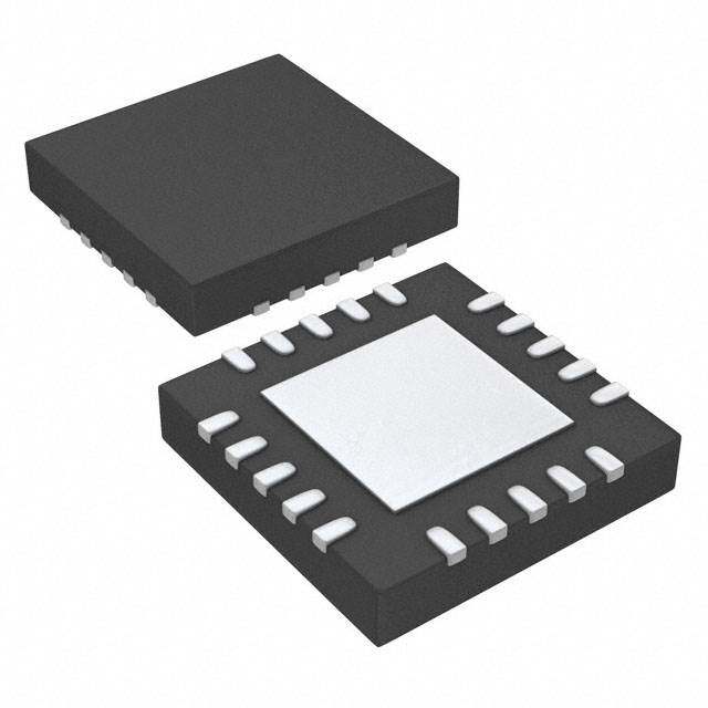
ICGOO电子元器件商城为您提供MAX1908ETI+由Maxim设计生产,在icgoo商城现货销售,并且可以通过原厂、代理商等渠道进行代购。 MAX1908ETI+价格参考。MaximMAX1908ETI+封装/规格:PMIC - 电池充电器, 多化学 充电器 IC 28-TQFN(5x5)。您可以下载MAX1908ETI+参考资料、Datasheet数据手册功能说明书,资料中有MAX1908ETI+ 详细功能的应用电路图电压和使用方法及教程。
Maxim Integrated的MAX1908ETI+是一款专用于电池充电管理的电源管理集成电路(PMIC),广泛应用于需要高效、可靠充电解决方案的便携式电子设备中。该芯片主要面向单节锂离子(Li+)或锂聚合物电池供电系统,常用于笔记本电脑、平板电脑、手持测试仪器以及工业便携设备等场景。

MAX1908ETI+支持外部MOSFET,允许设计者灵活配置充电电流和电压参数,适应不同容量电池的需求。其具备高精度的电流和电压调节功能,确保充电过程安全高效。此外,该器件集成过温保护、过流保护及输入电源限流功能,提升了系统的稳定性和安全性。

在应用场景中,MAX1908ETI+特别适合使用AC适配器或高电压USB电源进行充电的设计,能够实现快速充电并延长电池寿命,是高性能便携设备中理想的电池充电管理解决方案。
| 参数 | 数值 |
| 产品目录 | 集成电路 (IC)半导体 |
| 描述 | IC CHARGER BATTERY 28-TQFN电池管理 Multichemistry Battery Chargers |
| 产品分类 | |
| 品牌 | Maxim Integrated |
| 产品手册 | |
| 产品图片 |
|
| rohs | 符合RoHS无铅 / 符合限制有害物质指令(RoHS)规范要求 |
| 产品系列 | 电源管理 IC,电池管理,Maxim Integrated MAX1908ETI+- |
| 数据手册 | |
| 产品型号 | MAX1908ETI+ |
| UVLO停止阈值 | 7.85 V |
| UVLO起动阈值 | 7 V |
| 产品培训模块 | http://www.digikey.cn/PTM/IndividualPTM.page?site=cn&lang=zhs&ptm=25703http://www.digikey.cn/PTM/IndividualPTM.page?site=cn&lang=zhs&ptm=25705 |
| 产品种类 | 电池管理 |
| 产品类型 | Charge Management |
| 供应商器件封装 | 28-TQFN (5x5) |
| 功能 | 充电管理 |
| 包装 | 管件 |
| 商标 | Maxim Integrated |
| 安装类型 | 表面贴装 |
| 安装风格 | SMD/SMT |
| 封装 | Tube |
| 封装/外壳 | 28-WFQFN 裸露焊盘 |
| 封装/箱体 | TQFN-28 |
| 工作温度 | -40°C ~ 85°C |
| 工作电源电压 | 2.5 V to 3.6 V |
| 工作电源电流 | 400 uA |
| 工厂包装数量 | 60 |
| 最大工作温度 | + 85 C |
| 最小工作温度 | - 40 C |
| 标准包装 | 1 |
| 温度监测 | No Temperature Monitoring |
| 电压-电源 | 8 V ~ 28 V |
| 电池化学 | 多化学 |
| 电池类型 | Li-Ion, Li-Polymer, NiCd, NiMH, Lead Acid, Universal |
| 电荷安全定时器 | Charge Safety Timers |
| 系列 | MAX1908 |
| 零件号别名 | MAX1908 |

.jpg)


- 商务部:美国ITC正式对集成电路等产品启动337调查
- 曝三星4nm工艺存在良率问题 高通将骁龙8 Gen1或转产台积电
- 太阳诱电将投资9.5亿元在常州建新厂生产MLCC 预计2023年完工
- 英特尔发布欧洲新工厂建设计划 深化IDM 2.0 战略
- 台积电先进制程称霸业界 有大客户加持明年业绩稳了
- 达到5530亿美元!SIA预计今年全球半导体销售额将创下新高
- 英特尔拟将自动驾驶子公司Mobileye上市 估值或超500亿美元
- 三星加码芯片和SET,合并消费电子和移动部门,撤换高东真等 CEO
- 三星电子宣布重大人事变动 还合并消费电子和移动部门
- 海关总署:前11个月进口集成电路产品价值2.52万亿元 增长14.8%


PDF Datasheet 数据手册内容提取
EVALUATION KIT AVAILABLE MAX1908/MAX8724/ AVAILABLE MAX8765/MAX8765A Low-Cost Multichemistry Battery Chargers General Description Features The MAX1908/MAX8724/MAX8765/MAX8765A highly (cid:1) ±0.5% Output Voltage Accuracy Using Internal integrated, multichemistry battery-charger control ICs Reference (±0.4% for MAX8765A, 2-/3-Cell Only) simplify the construction of accurate and efficient charg- ers. These devices use analog inputs to control charge (cid:1) ±4% Accurate Input Current Limiting current and voltage, and can be programmed by the host (cid:1) ±5% Accurate Charge Current or hardwired. The MAX1908/MAX8724/MAX8765/ MAX8765A achieve high efficiency using a buck topology (cid:1) Analog Inputs Control Charge Current and with synchronous rectification. Charge Voltage The MAX1908/MAX8724/MAX8765/MAX8765A feature (cid:1) Outputs for Monitoring input current limiting. This feature reduces battery Current Drawn from AC Adapter charge current when the input current limit is reached Charging Current to avoid overloading the AC adapter when supplying AC Adapter Presence the load and the battery charger simultaneously. The (cid:1) Up to 17.6V Battery-Voltage Set Point MAX1908/MAX8724/MAX8765/MAX8765A provide out- puts to monitor current drawn from the AC adapter (DC (cid:1) Maximum 28V Input Voltage input source), battery-charging current, and the pres- (cid:1) > 95% Efficiency ence of an AC adapter. The MAX1908’s conditioning charge feature provides 300mA to safely charge deeply (cid:1) Shutdown Control Input discharged lithium-ion (Li+) battery packs. (cid:1) Charge Any Battery Chemistry The MAX1908 includes a conditioning charge feature Li+, NiCd, NiMH, Lead Acid, etc. while the MAX8724/MAX8765/MAX8765Ado not. Ordering Information The MAX1908/MAX8724/MAX8765/MAX8765A charge two to four series Li+ cells, providing more than 5A, and are PART TEMP RANGE PIN-PACKAGE available in a space-saving, 28-pin, thin QFN package (5mm ×5mm). An evaluation kit is available to speed designs. MAX1908ETI+ -40°C to +85°C 28 Thin QFN-EP* Applications MAX8724ETI+ -40°C to +85°C 28 Thin QFN-EP* Notebook and Subnotebook Computers MAX8765ETI+ -40°C to +85°C 28 Thin QFN-EP* Personal Digital Assistants MAX8765AETI+ -40°C to +85°C 28 Thin QFN-EP* Handheld TermFinualnsctional Diagrams +Denotes a lead(Pb)-free/RoHS-compliant package. Minimum Operating Circuit *EP = Exposed pad. Pin Configuration AC ADAPTER TO EXTERNAL INPUT 0.01Ω LOAD TOP VIEW DCINCSSP CSSCNELLDLOS DLO PGND CSIP CSIN CELLS BATT VCTL REFIN 21 20 19 18 17 16 15 LDO VCTL BST ICTL DLOV DLOV 22 14 GND ACIN LX 23 13 ICTL MAX1908 ACOK MAX8724 DHI BST 24 12 REFIN MAX8765 FROM HOST µP SHDN MAX8765A LX DHI 25 MAX1908 11 ACOK ICHG DLO 10µH CSSN 26 MMAAXX88772645 10 ACIN IINP PGND MAX8765A CSSP 27 9 ICHG CCV CSIP IINP 28 8 SHDN CCI 0.015Ω CCS CSIN + BATT BATT+ 1 2 3 4 5 6 7 Pin Configurations appREeFarC LaSt eGnNDd of data sheet. Functional Diagrams continued at end of data sheet. DCIN LDO CLS REF CCS CCI CCV UCSP is a trademark of Maxim Integrated Products, Inc. THIN QFN For pricing, delivery, and ordering information, please contact Maxim Direct at 1-888-629-4642, or visit Maxim’s website at www.maximintegrated.com. 19-2764; Rev 5; 11/09
MAX1908/MAX8724/MAX8765/MAX8765A Low-Cost Multichemistry Battery Chargers ABSOLUTE MAXIMUM RATINGS DCIN, CSSP, CSSN, ACOKto GND.......................-0.3V to +30V DLOV, VCTL, ICTL, REFIN, CELLS, CLS, BST to GND............................................................-0.3V to +36V LDO, SHDNto GND.............................................-0.3V to +6V BST to LX..................................................................-0.3V to +6V DLOV to LDO.........................................................-0.3V to +0.3V DHI to LX...................................................-0.3V to (VBST+ 0.3V) DLO to PGND.........................................-0.3V to (VDLOV+ 0.3V) LX to GND.................................................................-6V to +30V LDO Short-Circuit Current...................................................50mA BATT, CSIP, CSIN to GND.....................................-0.3V to +20V Continuous Power Dissipation (TA= +70°C) CSIP to CSIN or CSSP to CSSN or 28-Pin Thin QFN (5mm ×5mm) PGND to GND....................................................-0.3V to +0.3V (derate 20.8mW/°C above +70°C) .........................1666.7mW CCI, CCS, CCV, DLO, ICHG, Operating Temperature Range ..........................-40°C to +85°C IINP, ACIN, REF to GND.......................-0.3V to (VLDO+ 0.3V) Junction Temperature......................................................+150°C Storage Temperature Range.............................-60°C to +150°C Lead Temperature (soldering, 10s).................................+300°C Stresses beyond those listed under “Absolute Maximum Ratings” may cause permanent damage to the device. These are stress ratings only, and functional operation of the device at these or any other conditions beyond those indicated in the operational sections of the specifications is not implied. Exposure to absolute maximum rating conditions for extended periods may affect device reliability. ELECTRICAL CHARACTERISTICS (VDCIN= VCSSP= VCSSN = 18V, VBATT= VCSIP= VCSIN= 12V, VREFIN= 3V, VVCTL= VICTL= 0.75 x VREFIN, CELLS = open, CLS = REF, VBST- VLX= 4.5V, ACIN = GND = PGND = 0, CLDO= 1µF, LDO = DLOV, CREF= 1µF; CCI, CCS, and CCV are compensated per Figure 1a; TA= 0°C to +85°C, unless otherwise noted. Typical values are at TA= +25°C.) PARAMETER SYMBOL CONDITIONS MIN TYP MAX UNITS CHARGE-VOLTAGE REGULATION Battery-Regulation Voltage VVCTL = VREFIN -0.5 + 0.5 A(McAcuXr1a9c0y8/MAX8724/MAX8765 VVCTL = VREFIN/20 -0.5 + 0.5 % (2, 3, or 4 Cells) and MAX8765A VVCTL = VLDO -0.5 + 0.5 (4 Cells Only)) Battery-Regulation Voltage VVCTL = VREFIN -0.4 + 0.4 Accuracy (MAX8765A, 2 or 3 VVCTL = VREFIN/20 -0.4 +0.4 % Cells Only) VVCTL = VLDO -0.4 +0.4 VCTL Default Threshold V VCTL rising 4.0 4.1 4.2 V REFIN Range ( Note 1) 2.5 3 .6 V REFIN Undervoltage Lockout V REFIN falling 1 .20 1.92 V CHARGE-CURRENT REGULATION CSIP-to-CSIN Full-Scale Current- V ICTL = VREFIN 71.25 75 78.75 mV Sense Voltage VICTL = VREFIN -5 + 5 VICTL = VREFIN x 0.6 -5 + 5 Charging-Current Accuracy VICTL = VLDO -6 + 6 % MAX8765/MAX8765A only; VICTL = VREFIN x -45 + 45 0.036 MAX8724 only; VICTL = VREFIN x 0.058 -33 + 33 Charge-Current Gain Error - 2 + 2 % (MAX8765/MAX8765A Only) Charge-Current Offset - 2 + 2 mV (MAX8765/MAX8765A Only) ICTL Default Threshold V ICTL rising 4.0 4.1 4.2 V BATT/CSIP/CSIN Input Voltage 0 1 9 V Range 2 Maxim Integrated
MAX1908/MAX8724/MAX8765/MAX8765A Low-Cost Multichemistry Battery Chargers ELECTRICAL CHARACTERISTICS (continued) (VDCIN= VCSSP= VCSSN = 18V, VBATT= VCSIP= VCSIN= 12V, VREFIN= 3V, VVCTL= VICTL= 0.75 x VREFIN, CELLS = open, CLS = REF, VBST- VLX= 4.5V, ACIN = GND = PGND = 0, CLDO= 1µF, LDO = DLOV, CREF= 1µF; CCI, CCS, and CCV are compensated per Figure 1a; TA= 0°C to +85°C, unless otherwise noted. Typical values are at TA= +25°C.) PARAMETER SYMBOL CONDITIONS MIN TYP MAX UNITS CSIP/CSIN Input Current VDCIN = 0V or VICTL = 0V or V SHDN = 0V 1 µA Charging 4 00 650 Cycle-by-Cycle Maximum Current R S2 = 0.015mΩ 6.0 6.8 7.5 A Limit ITChTreLs Phoowlde Vr-oDltoawgne Mode V VCTL rising REFIN/ REFIN/ REFIN/ V 100 55 33 (MAX1908/MAX8724 Only) ICTL, VCTL Input Bias Current VVCTL = VICTL = 0 or 3V -1 + 1 µA VDCIN = 0V, VVCTL = VICTL = VREFIN = 5V -1 + 1 REFIN Input Bias Current VDCIN = 5V, VREFIN = 3V -1 + 1 µA VREFIN = 5V -1 + 1 ICHG Transconductance GICHG VCSIP - VCSIN = 45mV 2.7 3 3.3 µA/mV (MAX1908/MAX8724 Only) ICHG Transconductance GICHG VCSIP - VCSIN = 45mV 2.85 3 3.15 µA/mV (MAX8765/MAX8765A Only) ICHG Transconductance Error -5 + 5 % (MAX8765/MAX8765A Only) ICHG Transconductance Offset -5 + 5 µA (MAX8765/MAX8765A Only) VCSIP - VCSIN = 75mV -6 + 6 ICHG Accuracy VCSIP - VCSIN = 45mV -5 + 5 % VCSIP - VCSIN = 5mV -40 + 40 ICHG Output Current V CSIP - VCSIN = 150mV, VICHG = 0V 350 µ A ICHG Output Voltage V CSIP - VCSIN = 150mV, ICHG = open 3.5 V INPUT-CURRENT REGULATION CSSP-to-CSSN Full-Scale 7 2 75 78 mV Current-Sense Voltage VCLS = VREF -4 + 4 Input Current-Limit Accuracy VCLS = VREF/2 -7.5 + 7.5 % V CLS = 1.1V (MAX8765/MAX8765A only) -10 + 10 Input Current-Limit Gain Error -2 + 2 % (MAX8765/MAX8765A Only) Input Current-Limit Offset -2 + 2 mV (MAX8765/MAX8765A Only) CSSP, CSSN Input Voltage 8 2 8 V Range CSSP, CSSN Input Current VDCIN = 0V 0 .1 1 µA (MAX1908/MAX8724 Only) V CSSP = VCSSN = VDCIN > 8V 3 50 600 C(MSASXP8 I7n6p5u/tM CAuXrr8e7n6t5A Only) V CSSP = VCSSN = 28V V VDDCCIINN == 02V8V 4 0 0.10 6 150 µA Maxim Integrated 3
MAX1908/MAX8724/MAX8765/MAX8765A Low-Cost Multichemistry Battery Chargers ELECTRICAL CHARACTERISTICS (continued) (VDCIN= VCSSP= VCSSN = 18V, VBATT= VCSIP= VCSIN= 12V, VREFIN= 3V, VVCTL= VICTL= 0.75 x VREFIN, CELLS = open, CLS = REF, VBST- VLX= 4.5V, ACIN = GND = PGND = 0, CLDO= 1µF, LDO = DLOV, CREF= 1µF; CCI, CCS, and CCV are compensated per Figure 1a; TA= 0°C to +85°C, unless otherwise noted. Typical values are at TA= +25°C.) PARAMETER SYMBOL CONDITIONS MIN TYP MAX UNITS C(MSASXN8 I7n6p5u/tM CAuXr8re7n6t5A Only) V CSSP = VCSSN = 28V V VDDCCIINN == 02V8V 00 ..11 1 1 µA CLS Input Range 1 .6 R EF V (MAX1908/MAX8724 Only) CLS Input Range 1 .1 R EF V (MAX8765/MAX8765A Only) CLS Input Bias Current V CLS = 2V -1 + 1 µA IINP Transconductance GIINP VCSSP - VCSSN = 75mV 2.7 3 3.3 µA/mV (MAX1908/MAX8724 Only) IINP Accuracy VCSSP - VCSSN = 75mV -5 + 5 % VCSSP - VCSSN = 37.5mV -7.5 + 7.5 IINP Transconductance GIINP VCSSP - VCCSN = 75mV 2.82 3 3.18 µA/mV (MAX8765/MAX8765A Only) IINP Transconductance Error - 6 + 6 % (MAX8765/MAX8765A Only) IINP Transconductance Offset -10 + 10 µA (MAX8765/MAX8765A Only) IINP Output Current V CSSP - VCSSN = 150mV, VIINP = 0V 350 µ A IINP Output Voltage V CSSP - VCSSN = 150mV, VIINP = open 3.5 V SUPPLY AND LDO REGULATOR DCIN Input Voltage Range VDCIN 8 2 8 V DCIN Undervoltage-Lockout Trip VDCIN falling 7 7.4 V Point VDCIN rising 7 .5 7.85 DCIN Quiescent Current IDCIN 8.0V < VDCIN < 28V 3 .2 6 mA BATT Input Current IBATT V VBBAATTTT == 21V9V to, V1D9CVI,N V =D C0IVN = 19.3V 2 0 0 51 00 µA LDO Output Voltage 8 V < VDCIN < 28V, no load 5.25 5.4 5.55 V LDO Load Regulation 0 < ILDO < 10mA 3 4 100 mV LDO Undervoltage-Lockout Trip V DCIN = 8V 3.20 4 5.15 V Point REFERENCE REF Output Voltage 0 < IREF < 500µA 4.072 4.096 4.120 V REF Undervoltage-Lockout Trip V REF falling 3 .1 3.9 V Point 4 Maxim Integrated
MAX1908/MAX8724/MAX8765/MAX8765A Low-Cost Multichemistry Battery Chargers ELECTRICAL CHARACTERISTICS (continued) (VDCIN= VCSSP= VCSSN = 18V, VBATT= VCSIP= VCSIN= 12V, VREFIN= 3V, VVCTL= VICTL= 0.75 x VREFIN, CELLS = open, CLS = REF, VBST- VLX= 4.5V, ACIN = GND = PGND = 0, CLDO= 1µF, LDO = DLOV, CREF= 1µF; CCI, CCS, and CCV are compensated per Figure 1a; TA= 0°C to +85°C, unless otherwise noted. Typical values are at TA= +25°C.) PARAMETER SYMBOL CONDITIONS MIN TYP MAX UNITS TRIP POINTS VDCIN falling, referred to VCSIN 50 100 150 (MAX1908/MAX8724 only) BATT Power-Fail Threshold mV VCSSP falling, referred to VCSIN 50 100 150 (MAX8765/MAX8765A only) BATT Power-Fail Threshold 2 00 m V Hysteresis ACIN rising (MAX8765/MAX8765A only) 2.028 2.048 2.068 ACIN Threshold V ACIN rising (MAX1908/MAX8724 only) 2.007 2.048 2.089 ACIN Threshold Hysteresis 0 .5% of REF 2 0 m V ACIN Input Bias Current V ACIN = 2.048V -1 + 1 µA SWITCHING REGULATOR DHI Off-Time VBATT = 16V, VDCIN = 19V, 0.36 0.4 0.44 µs VCELLS = VREFIN DHI Minimum Off-Time VBATT = 16V, VDCIN = 17V, 0.24 0.28 0.33 µs VCELLS = VREFIN DHI Maximum On-Time 2 .5 5 7.5 ms DLOV Supply Current D LO low 5 10 µA BST Supply Current D HI high 6 15 µA BST Input Quiescent Current VDCIN = 0V, VBST = 24.5V, 0 .3 1 µA VBATT = VLX = 20V LX Input Bias Current V DCIN = 28V, VBATT = VLX = 20V 1 50 500 µA LX Input Quiescent Current V DCIN = 0V, VBATT = VLX = 20V 0 .3 1 µA DHI Maximum Duty Cycle 9 9 99.9 % Minimum Discontinuous-Mode 0 .5 A Ripple Current Battery Undervoltage Charge VBATT = 3V per cell (RS2 = 15mΩ), 150 300 450 mA Current MAX1908 only, VBATT rising CELLS = GND, MAX1908 only, VBATT rising 6.1 6.2 6.3 Battery Undervoltage Current CELLS = open, MAX1908 only, VBATT rising 9.15 9.3 9.45 V Threshold CELLS = VREFIN, MAX1908 only, VBATT rising 12.2 12.4 12.6 DHI On-Resistance High V BST - VLX = 4.5V, IDHI = +100mA 4 7 Ω DHI On-Resistance Low V BST - VLX = 4.5V, IDHI = -100mA 1 3.5 Ω DLO On-Resistance High V DLOV = 4.5V, IDLO = +100mA 4 7 Ω DLO On-Resistance Low V DLOV = 4.5V, IDLO = -100mA 1 3.5 Ω Maxim Integrated 5
MAX1908/MAX8724/MAX8765/MAX8765A Low-Cost Multichemistry Battery Chargers ELECTRICAL CHARACTERISTICS (continued) (VDCIN= VCSSP= VCSSN = 18V, VBATT= VCSIP= VCSIN= 12V, VREFIN= 3V, VVCTL= VICTL= 0.75 x VREFIN, CELLS = open, CLS = REF, VBST- VLX= 4.5V, ACIN = GND = PGND = 0, CLDO= 1µF, LDO = DLOV, CREF= 1µF; CCI, CCS, and CCV are compensated per Figure 1a; TA= 0°C to +85°C, unless otherwise noted. Typical values are at TA= +25°C.) PARAMETER SYMBOL CONDITIONS MIN TYP MAX UNITS ERROR AMPLIFIERS GMV Amplifier Transconductance GMV VV C T L = VL DO , V BAT T = 16.8V, 0.0625 0.125 0.2500 µA/mV CE L LS = V REF IN GMI Amplifier Transconductance GMI VICTL = VR EF IN, VCSIP - VCSIN = 75mV 0.5 1 2.0 µA/mV GMS Amplifier Transconductance GMS VCLS = VREF, VCSSP - VCSSN = 75mV 0.5 1 2.0 µA/mV CCI, CCS, CCV Clamp Voltage 0 .25V < VCCV,CCS,CCI < 2V 150 300 600 mV LOGIC LEVELS CELLS Input Low Voltage 0 .4 V CELLS Input Open Voltage C ELLS = open (/2V)R -EFIN V R EF IN / ( V/R2 ) E F + IN V 2 0.2V 0.2V CELLS Input High Voltage VREFIN V - 0.4V CELLS Input Bias Current C ELLS = 0V or VR EF IN -2 + 2 µA ACOK AND SHDN ACOK Input Voltage Range 0 2 8 V ACOK Sink Current V A COK = 0.4V, VACIN = 3V 1 m A ACOK Leakage Current V A COK = 28V, VACIN = 0V 1 µA SHDN Input Voltage Range 0 L DO V VSHDN = 0V OR VLDO -1 + 1 SHDN Input Bias Current µA VSHDN = 0V OR VSHDN = 5V -1 + 1 SHDN Threshold V S HDN falling 22 23.5 25 % of VREFIN SHDN Threshold Hysteresis 1 % of VREFIN 6 Maxim Integrated
MAX1908/MAX8724/MAX8765/MAX8765A Low-Cost Multichemistry Battery Chargers ELECTRICAL CHARACTERISTICS (VDCIN= VCSSP= VCSSN = 18V, VBATT= VCSIP= VCSIN= 12V, VREFIN= 3V, VVCTL= VICTL= 0.75 x VREFIN, CELLS = open, CLS = REF, VBST- VLX= 4.5V, ACIN = GND = PGND = 0, CLDO= 1µF, LDO = DLOV, CREF= 1µF; CCI, CCS, and CCV are compensated per Figure1a; TA= -40°C to +85°C, unless otherwise noted.) (Note 2) PARAMETER SYMBOL CONDITIONS MIN TYP MAX UNITS CHARGE-VOLTAGE REGULATION VVCTL = VREFIN -0.6 + 0.6 Battery Regulation Voltage VVCTL = VREFIN/20 -0.6 + 0.6 % Accuracy (2, 3, or 4 Cells) VVCTL = VLDO -0.6 + 0.6 REFIN Range ( Note 1) 2.5 3 .6 V REFIN Undervoltage Lockout V REFIN falling 1 .92 V CHARGE CURRENT REGULATION CSIP-to-CSIN Full-Scale Current- V ICTL = VREFIN 70.5 7 9.5 mV Sense Voltage VICTL = VREFIN -6 + 6 VICTL = VREFIN x 0.6 -7.5 + 7.5 VICTL = VLDO -7.5 + 7.5 Charging-Current Accuracy MAX8765/MAX8765A only; VICTL = VREFIN x -50 + 50 % 0.036 MAX8724 only; -33 + 33 VICTL = VREFIN x 0.058 Charge-Current Gain Error -2 + 2 % (MAX8765/MAX8765A Only) Charge-Current Offset -2 + 2 mV (MAX8765/MAX8765A Only) BATT/CSIP/CSIN Input Voltage 0 1 9 V Range CSIP/CSIN Input Current VDCIN = 0V or VICTL = 0V or VSHDN = 0V 1 µA Charging 6 50 Cycle-by-Cycle Maximum Current IMAX RS2 = 0.015Ω 6.0 7 .5 A Limit ITChTreLs Phoowlde Vr-oDltoawgne Mode V ICTL rising REFIN/ REFIN/ V 100 33 (MAX1908/MAX8724 Only) ICHG Transconductance GICHG VCSIP - VCSIN = 45mV 2.7 3 .3 µA/mV (MAX1908/MAX8724 Only) ICHG Transconductance GICHG VCSIP - VCSIN = 45mV 2.785 3 .225 µA/mV (MAX8765/MAX8765A Only) ICHG Transconductance Error - 7.5 + 7.5 % (MAX8765/MAX8765A Only) ICHG Transconductance Offset - 6.5 + 6.5 µA (MAX8765/MAX8765A Only) Maxim Integrated 7
MAX1908/MAX8724/MAX8765/MAX8765A Low-Cost Multichemistry Battery Chargers ELECTRICAL CHARACTERISTICS (continued) (VDCIN= VCSSP= VCSSN = 18V, VBATT= VCSIP= VCSIN= 12V, VREFIN= 3V, VVCTL= VICTL= 0.75 x VREFIN, CELLS = open, CLS = REF, VBST- VLX= 4.5V, ACIN = GND = PGND = 0, CLDO= 1µF, LDO = DLOV, CREF= 1µF; CCI, CCS, and CCV are compensated per Figure 1a; TA= -40°C to +85°C, unless otherwise noted.) (Note 2) PARAMETER SYMBOL CONDITIONS MIN TYP MAX UNITS VCSIP - VCSIN = 75mV -7.5 + 7.5 ICHG Accuracy VCSIP - VCSIN = 45mV -7.5 + 7.5 % VCSIP - VCSIN = 5mV -40 + 40 INPUT-CURRENT REGULATION CSSP-to-CSSN Full-Scale 7 1.25 7 8.75 mV Current-Sense Voltage VCLS = VREF -5 + 5 Input Current-Limit Accuracy VCLS = VREF/2 -7.5 + 7.5 % VCLS = 1.1V (MAX8765/MAX8765A only) -10 + 10 Input Current-Limit Gain Error - 2 + 2 % (MAX8765/MAX8765A Only) Input Current-Limit Offset - 2 + 2 mV (MAX8765/MAX8765A Only) CSSP, CSSN Input Voltage 8 2 8 V Range CSSP, CSSN Input Current VDCIN = 0V 1 µA (MAX1908/MAX8724 Only) VCSSP = VCSSN = VDCIN > 8V 6 00 C(MSASXP8 I7n6p5u/tM CAuXrr8e7n6t5A Only) V CSSP = VCSSN = 28V V VDDCCIINN == 208VV 6 150 µA C(MSASXN8 I7n6p5u/tM CAuXr8re7n6t5A Only) V CSSP = VCSSN = 28V V VDDCCIINN == 02V8V 11 µA CLS Input Range 1 .6 R EF V (MAX1908/MAX8724 Only) CLS Input Range 1 .1 R EF V (MAX8765/MAX8765A Only) IINP Transconductance GIINP VCSSP - VCSSN = 75mV 2.7 3 .3 µA/mV (MAX1908/MAX8724 Only) IINP Transconductance GIINP VCSSP - VCCSN = 75mV 2.785 3 .225 µA/mV (MAX8765/MAX8765A Only) IINP Transconductance Error - 7.5 + 7.5 % (MAX8765/MAX8765A Only) IINP Transconductance Offset -12 + 12 µA (MAX8765/MAX8765A Only) IINP Accuracy VCSSP - VCSSN = 75mV -7.5 + 7.5 % VCSSP - VCSSN = 37.5mV -7.5 + 7.5 8 Maxim Integrated
MAX1908/MAX8724/MAX8765/MAX8765A Low-Cost Multichemistry Battery Chargers ELECTRICAL CHARACTERISTICS (continued) (VDCIN= VCSSP= VCSSN = 18V, VBATT= VCSIP= VCSIN= 12V, VREFIN= 3V, VVCTL= VICTL= 0.75 x VREFIN, CELLS = open, CLS = REF, VBST- VLX= 4.5V, ACIN = GND = PGND = 0, CLDO= 1µF, LDO = DLOV, CREF= 1µF; CCI, CCS, and CCV are compensated per Figure 1a; TA= -40°C to +85°C, unless otherwise noted.) (Note 2) PARAMETER SYMBOL CONDITIONS MIN TYP MAX UNITS SUPPLY AND LDO REGULATOR DCIN Input Voltage Range VDCIN 8 2 8 V DCIN Quiescent Current IDCIN 8.0V < VDCIN < 28V 6 mA BATT Input Current IBATT V VBBAATTTT == 21V9V to, V1D9CVI,N V =D C0IVN = 19.3V 5 1 00 µA LDO Output Voltage 8 V < VDCIN < 28V, no load 5.25 5 .55 V LDO Load Regulation 0 < ILDO < 10mA 1 00 mV REFERENCE REF Output Voltage 0 < IREF < 500µA 4.065 4 .120 V TRIP POINTS VDCIN falling, referred to VCSIN 50 1 50 (MAX1908/MAX8724 only) BATT Power-Fail Threshold mV VCSSP falling, referred to VCSIN 50 1 50 (MAX8765/MAX8765A only) ACIN Threshold ACIN rising (MAX8765/MAX8765A only) 2.028 2 .068 V ACIN rising (MAX1908/MAX8724 only) 2.007 2 .089 SWITCHING REGULATOR DHI Off-Time VBATT = 16V, VDCIN = 19V, 0.35 0 .45 µs VCELLS = VREFIN DHI Minimum Off-Time VBATT = 16V, VDCIN = 17V, 0.24 0 .33 µs VCELLS = VREFIN DHI Maximum On-Time 2 .5 7 .5 ms DHI Maximum Duty Cycle 9 9 % Battery Undervoltage Charge VBATT = 3V per cell (RS2 = 15mΩ), 150 4 50 mA Current MAX1908 only, VBATT rising CELLS = GND, MAX1908 only, VBATT rising 6.09 6 .30 Battery Undervoltage Current CELLS = open, MAX1908 only, VBATT rising 9.12 9 .45 V Threshold CELLS = VREFIN, MAX1908 only, VBATT rising 12.18 1 2.60 DHI On-Resistance High V BST - VLX = 4.5V, IDHI = +100mA 7 Ω DHI On-Resistance Low V BST - VLX = 4.5V, IDHI = -100mA 3 .5 Ω DLO On-Resistance High V DLOV = 4.5V, IDLO = +100mA 7 Ω DLO On-Resistance Low V DLOV = 4.5V, IDLO = -100mA 3 .5 Ω Maxim Integrated 9
MAX1908/MAX8724/MAX8765/MAX8765A Low-Cost Multichemistry Battery Chargers ELECTRICAL CHARACTERISTICS (continued) (VDCIN= VCSSP= VCSSN = 18V, VBATT= VCSIP= VCSIN= 12V, VREFIN= 3V, VVCTL= VICTL= 0.75 x VREFIN, CELLS = open, CLS = REF, VBST- VLX= 4.5V, ACIN = GND = PGND = 0, CLDO= 1µF, LDO = DLOV, CREF= 1µF; CCI, CCS, and CCV are compensated per Figure 1a; TA= -40°C to +85°C, unless otherwise noted.) (Note 2) PARAMETER SYMBOL CONDITIONS MIN TYP MAX UNITS ERROR AMPLIFIERS GMV Amplifier Transconductance GMV VV C T L = VL DO , V BAT T = 16.8V, 0.0625 0 .250 µA/mV CE L LS = V REF IN GMI Amplifier Transconductance GMI VICTL = VR EF IN, VCSIP - VCSIN = 75mV 0.5 2 .0 µA/mV GMS Amplifier Transconductance GMS VCLS = VREF, VCSSP - VCSSN = 75mV 0.5 2 .0 µA/mV CCI, CCS, CCV Clamp Voltage 0 .25V < VCCV,CCS,CCI < 2V 150 6 00 mV LOGIC LEVELS CELLS Input Low Voltage 0 .4 V (VREFIN ( VR EF IN CELLS Input Open Voltage C ELLS = open /2) - /2) + V 0.2V 0.2V CELLS Input High Voltage VREFIN V - 0.4V ACOK AND SHDN ACOK Input Voltage Range 0 2 8 V ACOK Sink Current V ACOK = 0.4V, VACIN = 3V 1 m A SHDN Input Voltage Range 0 L DO V SHDN Threshold V SHDN falling 22 2 5 V %RE oFIfN Note 1: If both ICTL and VCTL use default mode (connected to LDO), REFIN is not used and can be connected to LDO. Note 2: Specifications to TA= -40°C are guaranteed by design and not production tested. Typical Operating Characteristics (Circuit of Figure 1, VDCIN= 20V, TA= +25°C, unless otherwise noted.) LOAD-TRANSIENT RESPONSE LOAD-TRANSIENT RESPONSE LOAD-TRANSIENT RESPONSE (BATTERY INSERTION AND REMOVAL) (STEP IN-LOAD CURRENT) (STEP IN-LOAD CURRENT) MAX1908 toc01 MAX1908 toc02 MAX1908 toc03 ADAPTER CURRENT LOAD IBATT 5A/div CURRENT 2A/div LOAD 0 5A/div 0 CURRENT ADAPTER VBATT 5A/div 0 CURRENT 5V/div CCV VBATT 16.8V 5A/div 0 2V/div CHARGE CCS CURRENT 500mVV/CdCivI CCI 500mVV/CdCivI CCI CCI 2A/div 0 500mVVC/CdiVv 500mVVC/dCiSv CCS 2VVB/AdTivT 1ms/div 1ms/div 1ms/div ICTL = LDO ICTL = LDO ICTL = LDO VCTL = LDO CHARGING CURRENT = 3A CHARGING CURRENT = 3A VBATT = 16.8V VBATT = 16.8V LOAD STEP = 0 TO 4A LOAD STEP = 0 TO 4A ISOURCE LIMIT = 5A ISOURCE LIMIT = 5A 10 Maxim Integrated
MAX1908/MAX8724/MAX8765/MAX8765A Low-Cost Multichemistry Battery Chargers Typical Operating Characteristics (continued) (Circuit of Figure1, VDCIN= 20V, TA= +25°C, unless otherwise noted.) LINE-TRANSIENT RESPONSE LDO LOAD REGULATION LDO LINE REGULATION MAX1908 toc04 0 0.05 10VVD/CdIiNv --00..12 MAX1908 toc05 00..0043 VILLDDOO = = 0 5.4V MAX1908 toc06 VBATT -0.3 0.02 500mV/div %) %) R ( -0.4 R (0.01 O O RR -0.5 RR 0 E E DO-0.6 DO-0.01 VL VL INDUCTOR -0.7 -0.02 CURRENT -0.8 -0.03 500mA/div VLDO = 5.4V -0.9 -0.04 -1.0 -0.05 10ms/div 0 1 2 3 4 5 6 7 8 9 10 8 10 12 14 16 18 20 22 24 26 28 ICTL = LDO VCTL = LDO LDO CURRENT (mA) VIN (V) ICHARGE = 3A LINE STEP 18.5V TO 27.5V REF VOLTAGE LOAD REGULATION REF VOLTAGE ERROR vs. TEMPERATURE EFFICIENCY vs. CHARGE CURRENT 0 0.10 100 --00..0021 MAX1908 toc07 00..0068 MAX1908 toc08 9800 MAX1908 toc09 -0.03 0.04 70 VBATT = 16V %) %) %) R (-0.04 R (0.02 Y ( 60 VBATT = 12V O O C RR-0.05 RR 0 EN 50 V EREF-0.06 V EREF-0.02 EFFICI 40 VBATT = 8V -0.07 -0.04 30 -0.08 -0.06 20 -0.09 -0.08 10 -0.10 -0.10 0 0 100 200 300 400 500 -40 -15 10 35 60 85 0.01 0.1 1 10 REF CURRENT (µA) TEMPERATURE (°C) CHARGE CURRENT (A) FREQUENCY vs. VIN - VBATT OUTPUT V/I CHARACTERISTICS BATT VOLTAGE ERROR vs. VCTL 445500000 3 CELLS MAX1908 toc10 000...345 3 CELLS2 CELLS MAX1908 toc11 00..0078 MAX1908 toc12 %) %) 0.06 CY (kHz) 330500 4 CELLS E ERROR ( 00..12 E ERROR ( 0.05 N 250 G 0 G 0.04 E A A U T T REQ 200 VOL -0.1 4 CELLS VOL 0.03 F 150 TT -0.2 TT A A 100 ICHARGE = 3A B -0.3 B 0.02 4 CELLS VCTL = ICTL = LDO REFIN = 3.3V 50 -0.4 0.01 NO LOAD 0 -0.5 0 0 2 4 6 8 10 12 14 16 18 20 22 0 1 2 3 4 0 0.1 0.2 0.3 0.4 0.5 0.6 0.7 0.8 0.9 1.0 (VIN - VBATT) (V) BATT CURRENT (A) VCTL/REFIN (%) Maxim Integrated 11
MAX1908/MAX8724/MAX8765/MAX8765A Low-Cost Multichemistry Battery Chargers Typical Operating Characteristics (continued) (Circuit of Figure1, VDCIN= 20V, TA= +25°C, unless otherwise noted.) CURRENT-SETTING ERROR vs. ICTL ICHG ERROR vs. CHARGE CURRENT %) 45 MAX1908 toc13 445...050 MAX1908 toc14 OR ( VREFIN = 3.3V 3.5 VREFIN = 3.3V R 3 T-SETTING ER 2 ICHG (%) 223...050 VVVBBBAAATTTTT T = == 1 1826VVV REN 1 1.5 R U C 1.0 0 0.5 -1 0 0 0.5 1.0 1.5 2.0 0 0.5 1.0 1.5 2.0 2.5 3.0 VICTL (V) IBATT (A) IINP ERROR vs. SYSTEM LOAD CURRENT IINP ERROR vs. INPUT CURRENT 3400 MAX1908 toc15 6800 MAX1908 toc16 20 40 ERROR DUE TO SWITCHING NOISE %) 10 IBATT = 0 %) 20 R ( R ( O O RR 0 RR 0 E E P P IIN -10 IIN -20 SYSTEM LOAD = 0 -20 -40 -30 -60 -40 -80 0 1 2 3 4 0 0.5 1.0 1.5 2.0 SYSTEM LOAD CURRENT (A) INPUT CURRENT (A) 12 Maxim Integrated
MAX1908/MAX8724/MAX8765/MAX8765A Low-Cost Multichemistry Battery Chargers Pin Description PIN NAME FUNCTION 1 DCIN Charging Voltage Input. Bypass DCIN with a 1µF capacitor to PGND. 2 LDO De vic e Po we r Su pp l y . Outpu t of the 5.4V li n ear re gu la tor supp l i e d fro m DC I N . Bypa ss wi t h a 1µF capa cit or to GND . 3 CLS Source Current-Limit Input. Voltage input for setting the current limit of the input source. 4 REF 4.096V Voltage Reference. Bypass REF with a 1µF capacitor to GND. 5 CCS Input-Current Regulation Loop-Compensation Point. Connect a 0.01µF capacitor to GND. 6 CCI Output-Current Regulation Loop-Compensation Point. Connect a 0.01µF capacitor to GND. 7 CCV Voltage Regulation Loop-Compensation Point. Connect 1kΩ in series with a 0.1µF capacitor to GND. 8 SHDN Shutdown Control Input. Drive SHDN logic low to shut down the MAX1908/MAX8724/MAX8765 MAX8765A. Use with a thermistor to detect a hot battery and suspend charging. Charge-Current Monitor Output. ICHG is a scaled-down replica of the charger output current. Use ICHG to 9 ICHG monitor the charging current and detect when the chip changes from constant-current mode to constant- voltage mode. The transconductance of (CSIP - CSIN) to ICHG is 3µA/mV. 10 ACIN AC Detect Input. Input to an uncommitted comparator. ACIN can be used to detect AC-adapter presence. 11 ACOK AC Detect Output. High-voltage open-drain output is high impedance when VACIN is less than VREF/2. 12 REFIN Reference Input. Allows the ICTL and VCTL inputs to have ratiometric ranges for increased accuracy. Output Current-Limit Set Input. ICTL input voltage range is VREFIN/32 to VREFIN. The MAX1908/MAX8724 shut 13 ICTL down if ICTL is forced below VREFIN/100 while the MAX8765/MAX8765A does not. When ICTL is equal to LDO, the set point for CSIP - CSIN is 45mV. 14 GND Analog Ground 15 VCTL Output Voltage-Limit Set Input. VCTL input voltage range is 0 to VREFIN. When VCTL is equal to LDO, the set point is (4.2 x CELLS)V. 16 BATT Battery Voltage Input 17 CELLS Cell Count Input. Tri-level input for setting number of cells. GND = 2 cells, open = 3 cells, REFIN = 4 cells. 18 CSIN Output Current-Sense Negative Input 19 CSIP Output Current-Sense Positive Input. Connect a current-sense resistor from CSIP to CSIN. 20 PGND Power Ground 21 DLO Low-Side Power MOSFET Driver Output. Connect to low-side nMOS gate. 22 DLOV Low-Side Driver Supply. Bypass DLOV with a 1µF capacitor to GND. 23 LX High-Side Power MOSFET Driver Power-Return Connection. Connect to the source of the high-side nMOS. 24 BST High-Side Power MOSFET Driver Power-Supply Connection. Connect a 0.1µF capacitor from LX to BST. 25 DHI High-Side Power MOSFET Driver Output. Connect to high-side nMOS gate. 26 CSSN Input Current-Sense Negative Input 27 CSSP Input Current-Sense Positive Input. Connect a current-sense resistor from CSSP to CSSN. 28 IINP Input-Current Monitor Output. IINP is a scaled-down replica of the input current. IINP monitors the total system current. The transconductance of (CSSP - CSSN) to IINP is 3µA/mV. Maxim Integrated 13
MAX1908/MAX8724/MAX8765/MAX8765A Low-Cost Multichemistry Battery Chargers Detailed Description voltage. By limiting the adjust range to 10% of the regu- lation voltage, the external resistor mismatch error is The MAX1908/MAX8724/MAX8765/MAX8765A include reduced from 1% to 0.05% of the regulation voltage. all the functions necessary to charge Li+ batteries. A Therefore, an overall voltage accuracy of better than high-efficiency synchronous-rectified step-down DC-DC 0.7% is maintained while using 1% resistors. The per- converter controls charging voltage and current. The cell battery termination voltage is a function of the bat- device also includes input-source current limiting and tery chemistry. Consult the battery manufacturer to analog inputs for setting the charge current and charge determine this voltage. Connect VCTL to LDO to select voltage. Control charge current and voltage using the the internal default setting VBATT = 4.2V × number of ICTL and VCTL inputs, respectively. Both ICTL and cells, or program the battery voltage with the following VCTL are ratiometric with respect to REFIN, allowing equation: compatibility with DACs or microcontrollers (µCs). Ratiometric ICTL and VCTL improve the accuracy of the ⎛ ⎛ V ⎞⎞ charge current and voltage set point by matching VRE- VBATT =CELLS×⎝⎜4V+⎝⎜0.4× VVCTL ⎠⎟⎠⎟ FIN to the reference of the host. For standard applica- REFIN tions, internal set points for ICTL and VCTL provide 3A charge current (with 0.015Ω sense resistor), and 4.2V CELLS is the programming input for selecting cell count. (per cell) charge voltage. Connect ICTL and VCTL to Connect CELLS as shown in Table 2 to charge 2, 3, or 4 LDO to select the internal set points. The MAX1908 Li+ cells. When charging other cell chemistries, use safely conditions overdischarged cells with 300mA (with CELLS to select an output voltage range for the charger. 0.015Ω sense resistor) until the battery-pack voltage The internal error amplifier (GMV) maintains voltage exceeds 3.1V × number of series-connected cells. The regulation (Figure 3). The voltage error amplifier is SHDN input allows shutdown from a microcontroller or compensated at CCV. The component values shown in thermistor. Figures 1 and 2 provide suitable performance for most The DC-DC converter uses external n-channel applications. Individual compensation of the voltage reg- MOSFETs as the buck switch and synchronous rectifier ulation and current regulation loops allows for optimal to convert the input voltage to the required charging compensation (see the Compensationsection). current and voltage. The Typical Application Circuit shown in Figure 1 uses a µC to control charging cur- Table 1. Versions Comparison rent, while Figure 2 shows a typical application with charging voltage and current fixed to specific values MAX8765/ for the application. The voltage at ICTL and the value of DESCRIPTION MAX1908 MAX8724 MAX8765A RS2 set the charging current. The DC-DC converter generates the control signals for the external MOSFETs Conditioning Yes No No to regulate the voltage and the current set by the VCTL, Charge Feature ICTL, and CELLS inputs. ICTL Shutdown Yes Yes No The MAX1908/MAX8724/MAX8765/MAX8765A feature Mode a voltage regulation loop (CCV) and two current regula- ACOK Enable REFIN must REFIN must Independent tion loops (CCI and CCS). The CCV voltage regulation Condition be ready be ready of REFIN loop monitors BATT to ensure that its voltage does not exceed the voltage set by VCTL. The CCI battery cur- rent regulation loop monitors current delivered to BATT Table 2. Cell-Count Programming to ensure that it does not exceed the current limit set by ICTL. A third loop (CCS) takes control and reduces the CELLS CELL COUNT battery-charging current when the sum of the system load and the battery-charging input current exceeds GND 2 the input current limit set by CLS. Open 3 Setting the Battery-Regulation Voltage VREFIN 4 The MAX1908/MAX8724/MAX8765/MAX8765A use a high-accuracy voltage regulator for charging voltage. The VCTL input adjusts the charger output voltage. VCTL control voltage can vary from 0 to VREFIN, provid- ing a 10% adjustment range on the VBATT regulation 14 Maxim Integrated
MAX1908/MAX8724/MAX8765/MAX8765A Low-Cost Multichemistry Battery Chargers Typical Application Circuits AC ADAPTER INPUT RS1 TO EXTERNAL 8.5V TO 28V D1 0.01Ω LOAD C1 2 × 10µF 0.1µF 0.1µF D2 CSSP CSSN R6 59kΩ R7 DCIN CELLS OPEN (3 CELLS SELECT) 1% 19.6kΩ C5 1% 1µF LDO C13 LDO VCTL 1µF R331Ω3 D3 BST DAC OUTPUT ICTL DLOV 12.6V OUTPUT VOLTAGE VCC REFIN C0.115µF C1µ16F R8 1MΩ ACIN DHI N1a ACOK LX OUTPUT SHDN N1b DLO ADC INPUT ICHG MAX1908 MAX8724 PGND L110µH MAX8765 ADC INPUT IINP MAX8765A CCV CSIP C14 R9 C20 R10 0.1µF 20kΩ 0.1µF 10kΩ R5 1kΩ RS2 HOST 0.015Ω C11 0.1µF CSIN CCI BATT BATT+ CCS C9 C10 GND C4 0.01µF 0.01µF REF CLS 22µF AVDD/REF R101k9Ω, R20, R21 1Cµ12F 7C.U5AR RINENPUT TLIMIT SMART BATTERY SCL SCL SDA SDA ADC INPUT TEMP GND BATT- PGND GND Figure 1. µC-Controlled Typical Application Circuit Maxim Integrated 15
MAX1908/MAX8724/MAX8765/MAX8765A Low-Cost Multichemistry Battery Chargers Typical Application Circuits (continued) AC ADAPTER INPUT RS1 TO EXTERNAL 8.5V TO 28V P1 0.01Ω LOAD R11 C1 15kΩ 2 × 10µF 0.01µF0.01µF R12 12kΩ REFIN (4 CELLS SELECT) R6 D2 CSSP CSSN 59kΩ ACOK 1% R7 DCIN CELLS LDO 19.6kΩ C5 1% 1µF LDO R14 LDO VCTL C13 110%.5kΩ 1µF R331Ω3 D3 REFIN BST R15 8.25kΩ DLOV 1% C15 C16 ICTL 0.1µF 1µF 16.8V OUTPUT VOLTAGE N1a R16 2.5A CHARGE LIMIT 8.25kΩ ACIN DHI 1% LX R19 C12 FROM HOST µP N 110%kΩ 1.5nF DLO N1b (SHUTDOWN) SHDN MAX1908 L1 MAX8724 PGND 10µH R20 10kΩ ICHG MAX8765 1% MAX8765A IINP CSIP CCV R5 1kΩ RS2 0.015Ω C11 0.1µF CSIN CCI BATT BATT+ CCS C9 C10 GND C4 BATTERY 0.01µF 0.01µF REF CLS 22µF THM BATT- C12 R17 1µF 19.1kΩ 1% PGND GND R18 22kΩ 1% 4A INPUT CURRENT LIMIT Figure 2. Typical Application Circuit with Fixed Charging Parameters 16 Maxim Integrated
MAX1908/MAX8724/MAX8765/MAX8765A Low-Cost Multichemistry Battery Chargers Functional Diagram DCIN SHDN 23.5% LDO REFIN GND RDY 5.4V 4.096V MAX1908 LINEAR REF LOGIC REFERENCE MAX8724 BLOCK REGULATOR GND MAX8765 MAX1908/MAX8724 ONLY MAX8765A 1/55 REFIN ICTL SRDY ACIN ACOK DCIN N REF/2 CCS 75mV CLS x REF GM IINP GMS CSSP LEVEL SHIFTER CSSN GM ICHG CSIP LEVEL CSI SHIFTER CSIN BST GMI 75mV ICTL x LEVEL REFIN SHIFTER DRIVER DHI CCI MAX1908 ONLY LX BATT 3.1V/CELL BAT_UV LVC LVC DC-DC REFIN R1 CONVERTER GMV CELL CELLS SELECT DLOV LOGIC DRIVER DLO CCV PGND 400mV VCTL x 4V REFIN Figure 3. Functional Diagram Maxim Integrated 17
MAX1908/MAX8724/MAX8765/MAX8765A Low-Cost Multichemistry Battery Chargers Setting the Charging-Current Limit threshold is exceeded, ensuring the battery charger The ICTL input sets the maximum charging current. The does not load down the AC adapter voltage. An internal current is set by current-sense resistor RS2, connected amplifier compares the voltage between CSSP and between CSIP and CSIN. The full-scale differential CSSN to the voltage at CLS. VCLS can be set by a voltage between CSIP and CSIN is 75mV; thus, for a resistive divider between REF and GND. Connect CLS 0.015Ω sense resistor, the maximum charging current to REF for the full-scale input current limit. The CLS volt- is 5A. Battery-charging current is programmed with age range for the MAX1908/MAX8724 is from 1.6V to ICTL using the equation: REF, while the MAX8765/MAX8765A CLS voltage is from 1.1V to REF. V 0.075 I = ICTL × The input current is the sum of the device current, the CHG VREFIN RS2 charger input current, and the load current. The device current is minimal (3.8mA) in comparison to the charge The input voltage range for ICTL is VREFIN/32 to VREFIN. and load currents. Determine the actual input current The MAX1908/MAX8724 shut down if ICTL is forced required as follows: below VREFIN/100 (min), while the MAX8765/MAX8765A dCooensn encott . ICTL to LDO to select the internal default full- IINPUT =ILOAD+⎛⎝⎜ICHGVIN××VBηATT⎞⎠⎟ scale, charge-current sense voltage of 45mV. The where ηis the efficiency of the DC-DC converter. charge current when ICTL = LDO is: VCLS determines the reference voltage of the GMS I = 0.045V error amplifier. Sense resistor RS1 and VCLS determine CHG RS2 the maximum allowable input current. Calculate the input current limit as follows: where RS2 is 0.015Ω, providing a charge-current set V 0.075 point of 3A. IINPUT = CLS × V RS1 REF The current at the ICHG output is a scaled-down replica Once the input current limit is reached, the charging of the battery output current being sensed across CSIP current is reduced until the input current is at the and CSIN (see theCurrent Measurementsection). desired threshold. When choosing the current-sense resistor, note that the When choosing the current-sense resistor, note that the voltage drop across this resistor causes further power voltage drop across this resistor causes further power loss, reducing efficiency. However, adjusting ICTL to loss, reducing efficiency. Choose the smallest value for reduce the voltage across the current-sense resistor RS1 that achieves the accuracy requirement for the can degrade accuracy due to the smaller signal to the input current-limit set point. input of the current-sense amplifier. The charging- current-error amplifier (GMI) is compensated at CCI Conditioning Charge (see the Compensation section). The MAX1908 includes a battery-voltage comparator that allows a conditioning charge of overdischarged Li+ Setting the Input Current Limit battery packs. If the battery-pack voltage is less than The total input current (from an AC adapter or other DC 3.1V × number of cells programmed by CELLS, the source) is a function of the system supply current and MAX1908 charges the battery with 300mA current when the battery-charging current. The input current regulator using sense resistor RS2 = 0.015Ω. After the limits the input current by reducing the charging battery voltage exceeds the conditioning charge thresh- current when the input current exceeds the input old, the MAX1908 resumes full-charge mode, charging current-limit set point. System current normally fluc- to the programmed voltage and current limits. The tuates as portions of the system are powered up or MAX8724/MAX8765/MAX8765A do not offer this feature. down. Without input current regulation, the source must be able to supply the maximum system current and the AC Adapter Detection maximum charger input current simultaneously. By using Connect the AC adapter voltage through a resistive the input current limiter, the current capability of the AC divider to ACIN to detect when AC power is available, adapter can be lowered, reducing system cost. as shown in Figure 1. ACIN voltage rising trip point is The MAX1908/MAX8724/MAX8765/MAX8765A limit the VREF/2 with 20mV hysteresis. ACOK is an open-drain battery charge current when the input current-limit output and is high impedance when ACIN is less than 18 Maxim Integrated
MAX1908/MAX8724/MAX8765/MAX8765A Low-Cost Multichemistry Battery Chargers VREF/2. Since ACOK can withstand 30V (max), ACOK DC-DC Converter can drive a p-channel MOSFET directly at the charger The MAX1908/MAX8724/MAX8765/MAX8765A employ input, providing a lower dropout voltage than a a buck regulator with a bootstrapped nMOS high-side Schottky diode (Figure 2). In the MAX1908/MAX8724 switch and a low-side nMOS synchronous rectifier. the ACOK comparator is enabled after REFIN is ready. CCV, CCI, CCS, and LVC Control Blocks In the MAX8765/MAX8765A, the ACOK comparator is The MAX1908/MAX8724/MAX8765/MAX8765A control independent of REFIN. input current (CCS control loop), charge current (CCI Current Measurement control loop), or charge voltage (CCV control loop), Use ICHG to monitor the battery-charging current being depending on the operating condition. sensed across CSIP and CSIN. The ICHG voltage is The three control loops, CCV, CCI, and CCS are brought proportional to the output current by the equation: together internally at the LVC amplifier (lowest voltage VICHG= ICHG x RS2 x GICHGx R9 clamp). The output of the LVC amplifier is the feedback where ICHG is the battery-charging current, GICHG is control signal for the DC-DC controller. The output of the the transconductance of ICHG (3µA/mV typ), and R9 is GMamplifier that is the lowest sets the output of the LVC the resistor connected between ICHG and ground. amplifier and also clamps the other two control loops to Leave ICHG unconnected if not used. within 0.3V above the control point. Clamping the other two control loops close to the lowest control loop ensures Use IINP to monitor the system input current being fast transition with minimal overshoot when switching sensed across CSSP and CSSN. The voltage of IINP is between different control loops. proportional to the input current by the equation: DC-DC Controller VIINP= IINPUTx RS1 x GIINPx R10 The MAX1908/MAX8724/MAX8765/MAX8765A feature a where IINPUTis the DC current being supplied by the AC variable off-time, cycle-by-cycle current-mode control adapter power, GIINP is the transconductance of IINP scheme. Depending upon the conditions, the MAX1908/ (3µA/mV typ), and R10 is the resistor connected between MAX8724/MAX8765/MAX8765A work in continuous or IINP and ground. ICHG and IINP have a 0 to 3.5V output discontinuous-conduction mode. voltage range. Leave IINP unconnected if not used. Continuous-Conduction Mode LDO Regulator With sufficient charger loading, the MAX1908/MAX8724/ LDO provides a 5.4V supply derived from DCIN and MAX8765/MAX8765A operate in continuous-conduction can deliver up to 10mA of load current. The MOSFET mode (inductor current never reaches zero) switching at drivers are powered by DLOV and BST, which must be 400kHz if the BATT voltage is within the following range: connected to LDO as shown in Figure 1. LDO supplies the 4.096V reference (REF) and most of the control cir- 3.1V x (number of cells) < VBATT< (0.88 x VDCIN) cuitry. Bypass LDO with a 1µF capacitor to GND. The operation of the DC-DC controller is controlled by the following four comparators as shown in Figure 4: Shutdown The MAX1908/MAX8724/MAX8765/MAX8765A feature • IMIN—Compares the control point (LVC) against a low-power shutdown mode. Driving SHDN low shuts 0.15V (typ). If IMIN output is low, then a new cycle down the MAX1908/MAX8724/MAX8765/MAX8765A. In cannot begin. shutdown, the DC-DC converter is disabled and CCI, • CCMP—Compares the control point (LVC) against the CCS, and CCV are pulled to ground. The IINP and charging current (CSI). The high-side MOSFET on- ACOKoutputs continue to function. time is terminated if the CCMP output is high. SHDN can be driven by a thermistor to allow automatic • IMAX—Compares the charging current (CSI) to 6A shutdown of the MAX1908/MAX8724/MAX8765/ (RS2 = 0.015Ω). The high-side MOSFET on-time is MAX8765A when the battery pack is hot. The shutdown terminated if the IMAX output is high and a new cycle falling threshold is 23.5% (typ) of VREFIN with 1% cannot begin until IMAX goes low. VREFIN hysteresis to provide smooth shutdown when • ZCMP—Compares the charging current (CSI) to driven by a thermistor. 333mA (RS2 = 0.015Ω). If ZCMP output is high, then both MOSFETs are turned off. Maxim Integrated 19
MAX1908/MAX8724/MAX8765/MAX8765A Low-Cost Multichemistry Battery Chargers DC-DC Functional Diagram 5ms S RESET CSSP AC ADAPTER BST MAX1908 CSS IMAX MAX8724 X20 RS1 LDO 1.8V R Q MAX8765 CSSN D3 MAX8765A BST N1a DHI R Q DHI CBST CCMP LX CHG S Q IMIN L1 0.15V DLO N1b DLO tOFF GENERATOR ZCMP CSIP 0.1V CSI RS2 X20 CSIN LVC GMS BATT COUT GMI BATTERY GMV SETV CELL CONTROL SETI SELECT CLS LOGIC CELLS CCS CCI CCV Figure 4. DC-DC Functional Diagram 20 Maxim Integrated
MAX1908/MAX8724/MAX8765/MAX8765A Low-Cost Multichemistry Battery Chargers In normal operation, the controller starts a new cycle by Discontinuous Conduction turning on the high-side n-channel MOSFET and The MAX1908/MAX8724/MAX8765/MAX8765A enter dis- turning off the low-side n-channel MOSFET. When the continuous-conduction mode when the output of the LVC charge current is greater than the control point (LVC), control point falls below 0.15V. For RS2 = 0.015Ω, this CCMP goes high and the off-time is started. The corresponds to 0.5A: off-time turns off the high-side n-channel MOSFET and turns on the low-side n-channel MOSFET. The opera- IMIN= 0.15V =0.5A tional frequency is governed by the off-time and is 20×RS2 dependent upon VDCIN and VBATT. The off-time is set by the following equations: for RS2 = 0.015Ω. V −V In discontinuous mode, a new cycle is not started until t =2.5µs× DCIN BATT the LVC voltage rises above 0.15V. Discontinuous- OFF VDCIN mode operation can occur during conditioning charge of overdischarged battery packs, when the charge cur- L×I rent has been reduced sufficiently by the CCS control t = RIPPLE loop, or when the battery pack is near full charge (con- ON VCSSN−VBATT stant-voltage-charging mode). MOSFET Drivers where: The low-side driver output DLO switches between V ×t PGND and DLOV. DLOV is usually connected through IRIPPLE = BATT OFF a filter to LDO. The high-side driver output DHI is boot- L strapped off LX and switches between VLX and VBST. When the low-side driver turns on, BST rises to one 1 diode voltage below DLOV. f = t +t Filter DLOV with a lowpass filter whose cutoff frequency ON OFF is approximately 5kHz (Figure 1): These equations result in fixed-frequency operation 1 1 over the most common operating conditions. f = = =4.8kHz C 2πRC 2π×33Ω×1µF At the end of the fixed off-time, another cycle begins if the control point (LVC) is greater than 0.15V, IMIN = high, and the peak charge current is less than 6A (RS2 Dropout Operation = 0.015Ω), IMAX = high. If the charge current exceeds The MAX1908/MAX8724/MAX8765/MAX8765A have 99% IMAX, the on-time is terminated by the IMAX compara- duty-cycle capability with a 5ms (max) on-time and 0.3µs tor. IMAX governs the maximum cycle-by-cycle current (min) off-time. This allows the charger to achieve dropout limit and is internally set to 6A (RS2 = 0.015Ω). IMAX performance limited only by resistive losses in the DC-DC protects against sudden overcurrent faults. converter components (D1, N1, RS1, and RS2, Figure 1). Replacing diode D1 with a p-channel MOSFET driven by If, during the off-time, the inductor current goes to zero, ACOK improves dropout performance (Figure 2). The ZCMP = high, both the high- and low-side MOSFETs dropout voltage is set by the difference between DCIN are turned off until another cycle is ready to begin. and CSIN. When the dropout voltage falls below 100mV, There is a minimum 0.3µs off-time when the (VDCIN - the charger is disabled; 200mV hysteresis ensures that VBATT) differential becomes too small. If VBATT ≥ 0.88 × the charger does not turn back on until the dropout volt- VDCIN, then the threshold for minimum off-time is age rises to 300mV. reached and the tOFF is fixed at 0.3µs. A maximum on- Compensation time of 5ms allows the controller to achieve > 99% duty Each of the three regulation loops—input current limit, cycle in continuous-conduction mode. The switching charging current limit, and charging voltage limit—are frequency in this mode varies according to the equation: compensated separately using CCS, CCI, and CCV, 1 f = respectively. L×I ( RIPPLE )+0.3µs V −V CSSN BATT Maxim Integrated 21
MAX1908/MAX8724/MAX8765/MAX8765A Low-Cost Multichemistry Battery Chargers where RLvaries with load according to RL= VBATT/ICHG. Output zero due to output capacitor ESR: BATT 1 GMOUT fZ_ESR = 2πR ×C ESR OUT The loop transfer function is given by: RESR RL LTF=GM ×R ×GMV×R × CCV OUT L OGMV ( )( ) GMV COUT 1+sCOUT×RESR 1+sCCV×RCV ( )( ) 1+sC ×R 1+sC ×R CV OGMV OUT L RCV ROGMV REF Assuming the compensation pole is a very low CCV frequency, and the output zero is a much higher fre- quency, the crossover frequency is given by: GMV×R ×GM f = CV OUT Figure 5. CCV Loop Diagram CO_CV 2πC OUT CCV Loop Definitions To calculate RCVand CCVvalues of the circuit of Figure 2: Compensation of the CCV loop depends on the para- Cells = 4 meters and components shown in Figure 5. CCV and RCV are the CCV loop compensation capacitor and COUT= 22µF series resistor. RESR is the equivalent series resistance VBATT= 16.8V (ESR) of the charger output capacitor (COUT). RL is the ICHG= 2.5A equivalent charger output load, where RL = VBATT/ GMV = 0.125µA/mV ICHG. The equivalent output impedance of the GMV GMOUT= 3.33A/V amplifier, ROGMV ≥ 10MΩ. The voltage amplifier ROGMV= 10MΩ transconductance, GMV = 0.125µA/mV. The DC-DC f = 400kHz converter transconductance, GMOUT= 3.33A/V: Choose crossover frequency to be 1/5th the 1 MAX1908’s 400kHz switching frequency: GM = OUT ACSI×RS2 GMV×R ×GM f = CV OUT =80kHz CO_CV 2πC where ACSI = 20, and RS2 is the charging current- OUT sense resistor in the Typical Application Circuits. Solving yields RCV= 26kΩ. The compensation pole is given by: Conservatively set RCV= 1kΩ, which sets the crossover 1 frequency at: f = P_CV 2πROGMV ×CCV fCO_CV= 3kHz Choose the output-capacitor ESR so the output-capacitor The compensation zero is given by: zero is 10 times the crossover frequency: fZ_CV = 2πRCV1×CCV RESR=2π×10×fCO1_CV×COUT =0.24Ω The output pole is given by: 1 f = =2.412MHz f = 1 Z_ESR 2πRESR×COUT P_OUT 2πR ×C L OUT 22 Maxim Integrated
MAX1908/MAX8724/MAX8765/MAX8765A Low-Cost Multichemistry Battery Chargers The 22µF ceramic capacitor has a typical ESR of CCI Loop Definitions 0.003Ω, which sets the output zero at 2.412MHz. Compensation of the CCI loop depends on the parame- The output pole is set at: ters and components shown in Figure 7. CCI is the CCI loop compensation capacitor. ACSI is the internal gain 1 of the current-sense amplifier. RS2 is the charge cur- f = =1.08kHz P_OUT 2πR ×C rent-sense resistor, RS2 = 15mΩ. ROGMI is the equiva- L OUT lent output impedance of the GMI amplifier ≥ 10MΩ. GMI is the charge-current amplifier transconductance where: = 1µA/mV. GMOUT is the DC-DC converter transcon- ∆V ductance = 3.3A/V. The CCI loop is a single-pole sys- RL = ∆IBATT =Battery ESR tem with a dominant pole compensation set by fP_CI: CHG 1 f = Set the compensation zero (fZ_CV) so it is equivalent to P_CI 2πROGMI×CCI the output pole (fP_OUT = 1.08kHz), effectively produc- ing a pole-zero cancellation and maintaining a single- The loop transfer function is given by: pole system response: fZ_CV = 2πRCV1×CCV LTF=GMOUT×ACSI×RS2×GMI1+sRROOGGMMII×CCI Since: 1 CCV =2πRCV×1.08kHz =147nF GMOUT = A 1×RS2 CSI Choose CCV = 100nF, which sets the compensation The loop transfer function simplifies to: zero (fZ_CV) at 1.6kHz. This sets the compensation pole: 1 R f = =0.16Hz LTF=GMI × OGMI P_CV 2πR ×C 1+sR ×C OGMV CV OGMI CI CCV LOOP GAIN CCV LOOP PHASE vs. FREQUENCY vs. FREQUENCY 80 -45 60 -60 40 S) -75 E N (dB) 20 DEGRE -90 GAI 0 SE ( A H P-105 -20 -120 -40 -60 -135 1 10 100 1k 10k 100k 1M 1 10 100 1k 10k 100k 1M FREQUENCY (Hz) FREQUENCY (Hz) Figure 6. CCV Loop Gain/Phase vs. Frequency Maxim Integrated 23
MAX1908/MAX8724/MAX8765/MAX8765A Low-Cost Multichemistry Battery Chargers To calculate the CCI loop compensation pole, CCI: GMI = 1µA/mV CSIP CSIN GMOUT= 3.33A/V GMOUT RS2 ROGMI= 10MΩ f = 400kHz CSI Choose crossover frequency fCO_CI to be 1/5th the MAX1908/MAX8724/MAX8765/MAX8765A switching frequency: CCI GMI GMI f = =80kHz CO_CI 2πC CI CCI ROGMI ICTL Solving for CCI, CCI= 2nF. To be conservative, set CCI = 10nF, which sets the crossover frequency at: Figure 7. CCI Loop Diagram GMI f = =16kHz The crossover frequency is given by: CO_CI 2π10nF GMI The compensation pole, fP_CIis set at: f = CO_CI 2πC CI GMI f = =0.0016Hz The CCI loop dominant compensation pole: P_CI 2πROGMI×CCI f = 1 CCS Loop Definitions P_CI 2πR ×C Compensation of the CCS loop depends on the parame- OGMI CI ters and components shown in Figure 9. CCS is the CCS where the GMI amplifier output impedance, ROGMI = loop compensation capacitor. ACSSis the internal gain of 10MΩ. the current-sense amplifier. RS1 is the input current- sense resistor, RS1 = 10mΩ. ROGMS is the equivalent output impedance of the GMS amplifier ≥10MΩ. GMS is CCI LOOP GAIN CCI LOOP PHASE vs. FREQUENCY vs. FREQUENCY 100 0 80 -15 60 -30 S) N (dB) 2400 DEGREE -45 GAI SE ( -60 0 HA P -75 -20 -40 -90 -60 -105 0.1 1 10 100 1k 10k 100k 1M 0.1 1 10 100 1k 10k 100k 1M FREQUENCY (Hz) FREQUENCY (Hz) 24 Maxim Integrated
MAX1908/MAX8724/MAX8765/MAX8765A Low-Cost Multichemistry Battery Chargers the charge-current amplifier transconductance = 1µA/mV. GMIN is the DC-DC converter transconductance = 3.3A/V. The CCS loop is a single-pole system with a dom- CSSP CSSN inant pole compensation set by fP_CS: GMIN RS1 1 f = P_CS 2πR ×C OGMS CS CSS The loop transfer function is given by: R CCS LTF=GM ×A ×RS1×GMS× OGMS IN CSS 1+sR ×C GMS OGMS CS Since: CCS ROGMS CLS 1 GM = IN A ×RS1 CSS Then, the loop transfer function simplifies to: Figure 9. CCS Loop Diagram LTF=GMS× ROGMS The CCS loop dominant compensation pole: 1+sR ×C OGMS CS 1 f = P_CS 2πR ×C OGMS CS The crossover frequency is given by: GMS where the GMS amplifier output impedance, ROGMS = fCO_CS = 2πC 10MΩ. CS To calculate the CCI loop compensation pole, CCS: GMS = 1µA/mV GMIN= 3.33A/V ROGMS= 10MΩ f = 400kHz CCS LOOP GAIN CCS LOOP PHASE vs. FREQUENCY vs. FREQUENCY 100 0 80 -15 60 -30 S) N (dB) 2400 DEGREE -45 GAI SE ( -60 0 HA P -75 -20 -40 -90 -60 -105 0.1 1 10 100 1k 10k 100k 1M 0.1 1 10 100 1k 10k 100k 1M FREQUENCY (Hz) FREQUENCY (Hz) Figure 10. CCS Loop Gain/Phase vs.Frequency Maxim Integrated 25
MAX1908/MAX8724/MAX8765/MAX8765A Low-Cost Multichemistry Battery Chargers Choose crossover frequency fCO_CS to be 1/5th the where: MAX1908/MAX8724/MAX8765/MAX8765A switching tOFF= 2.5µs ×(VDCIN– VBATT)/VDCIN frequency: VBATT< 0.88 ×VDCIN GMS or: f = =80kHz CO_CS 2πCCS tOFF= 0.3µs VBATT> 0.88 ×VDCIN Solving for CCS, CCS= 2nF. Figure 11 illustrates the variation of ripple current vs. To be conservative, set CCS = 10nF, which sets the battery voltage when charging at 3A with a fixed 19V crossover frequency at: input voltage. Higher inductor values decrease the ripple current. GMS fCO_CS = 2π10nF =16kHz Smaller inductor values require higher saturation cur- rent capabilities and degrade efficiency. Designs for ripple current, IRIPPLE = 0.3 × ICHG usually result in a The compensation pole, fP_CSis set at: good balance between inductor size and efficiency. 1 Input Capacitor fP_CS=2πR ×C = 0.0016Hz Input capacitor C1 must be able to handle the input OGMS CS ripple current. At high charging currents, the DC-DC converter operates in continuous conduction. In this Component Selection case, the ripple current of the input capacitor can be Table 3 lists the recommended components and refers approximated by the following equation: to the circuit of Figure 2. The following sections describe how to select these components. I =I D−D2 Inductor Selection C1 CHG Inductor L1 provides power to the battery while it is where: being charged. It must have a saturation current of at least the charge current (ICHG), plus 1/2 the current rip- IC1= input capacitor ripple current. ple IRIPPLE: D = DC-DC converter duty ratio. ISAT= ICHG+ (1/2) IRIPPLE ICHG= battery-charging current. Ripple current varies according to the equation: Input capacitor C1 must be sized to handle the maxi- IRIPPLE= (VBATT) ×tOFF/L mum ripple current that occurs during continuous con- duction. The maximum input ripple current occurs at 50% duty cycle; thus, the worst-case input ripple cur- RIPPLE CURRENT vs. rent is 0.5 × ICHG. If the input-to-output voltage ratio is BATTERY VOLTAGE such that the DC-DC converter does not operate at a 1.5 50% duty cycle, then the worst-case capacitor current 3 CELLS occurs where the duty cycle is nearest 50%. The input capacitor ESR times the input ripple current T (A) 1.0 4 CELLS sets the ripple voltage at the input, and should not N RE exceed 0.5V ripple. Choose the ESR of C1 according to: R U C E RIPPL 0.5 ESRC1< 0.5V I C1 VDCIN = 19V VCTL = ICTL = LDO The input capacitor size should allow minimal output 0 voltage sag at the highest switching frequency: 8 9 10 11 12 13 14 15 16 17 18 VBATT (V) IC1 =C1dV 2 dt Figure 11. Ripple Current vs. Battery Voltage 26 Maxim Integrated
MAX1908/MAX8724/MAX8765/MAX8765A Low-Cost Multichemistry Battery Chargers where dV is the maximum voltage sag of 0.5V while the MOSFET. Choose N1b with either an internal delivering energy to the inductor during the high-side Schottky diode or body diode capable of carrying the MOSFET on-time, and dt is the period at highest oper- maximum charging current during the dead time. The ating frequency (400kHz): Schottky diode D3 provides the supply current to the high-side MOSFET driver. I 2.5µs C1> C1 × Layout and Bypassing 2 0.5V Both tantalum and ceramic capacitors are suitable in Bypass DCIN with a 1µF capacitor to power ground most applications. For equivalent size and voltage (Figure 1). D2 protects the MAX1908/MAX8724/ rating, tantalum capacitors have higher capacitance, MAX8765/MAX8765A when the DC power source input but also higher ESR than ceramic capacitors. This is reversed. A signal diode for D2 is adequate because makes it more critical to consider ripple current and DCIN only powers the internal circuitry. Bypass LDO, power-dissipation ratings when using tantalum capaci- REF, CCV, CCI, CCS, ICHG, and IINP to analog tors. A single ceramic capacitor often can replace two ground. Bypass DLOV to power ground. tantalum capacitors in parallel. Good PC board layout is required to achieve specified noise, efficiency, and stable performance. The PC Output Capacitor board layout artist must be given explicit instructions— The output capacitor absorbs the inductor ripple cur- preferably, a pencil sketch showing the placement of rent. The output capacitor impedance must be signifi- the power-switching components and high-current rout- cantly less than that of the battery to ensure that it ing. Refer to the PC board layout in the MAX1908 eval- absorbs the ripple current. Both the capacitance and uation kit for examples. Separate analog and power ESR rating of the capacitor are important for its effec- grounds are essential for optimum performance. tiveness as a filter and to ensure stability of the DC-DC converter (see the Compensationsection). Either tanta- Use the following step-by-step guide: lum or ceramic capacitors can be used for the output 1) Place the high-power connections first, with their filter capacitor. grounds adjacent: MOSFETs and Diodes a)Minimize the current-sense resistor trace lengths, Schottky diode D1 provides power to the load when the and ensure accurate current sensing with Kelvin AC adapter is inserted. This diode must be able to connections. deliver the maximum current as set by RS1. For b)Minimize ground trace lengths in the high-current reduced power dissipation and improved dropout per- paths. formance, replace D1 with a p-channel MOSFET (P1) c)Minimize other trace lengths in the high-current as shown in Figure 2. Take caution not to exceed the paths. maximum VGS of P1. Choose resistors R11 and R12 to limit the VGS. d)Use > 5mm wide traces. The n-channel MOSFETs (N1a, N1b) are the switching e)Connect C1 to high-side MOSFET (10mm max devices for the buck controller. High-side switch N1a length). should have a current rating of at least the maximum f) LX node (MOSFETs, inductor (15mm max charge current plus one-half the ripple current and length)). have an on-resistance (RDS(ON)) that meets the power Ideally, surface-mount power components are flush dissipation requirements of the MOSFET. The driver for against one another with their ground terminals N1a is powered by BST. The gate-drive requirement for almost touching. These high-current grounds are N1a should be less than 10mA. Select a MOSFET with a then connected to each other with a wide, filled zone low total gate charge (QGATE) and determine the required drive current by IGATE = QGATE × f (where f is of top-layer copper, so they do not go through vias. the DC-DC converter’s maximum switching frequency). The resulting top-layer power ground plane is connected to the normal ground plane at the The low-side switch (N1b) has the same current rating MAX1908/MAX8724/MAX8765/MAX8765As’ back- and power dissipation requirements as N1a, and side exposed pad. Other high-current paths should should have a total gate charge less than 10nC. N2 is also be minimized, but focusing primarily on short used to provide the starting charge to the BST capacitor ground and current-sense connections eliminates (C15). During the dead time (50ns, typ) between N1a most PC board layout problems. and N1b, the current is carried by the body diode of Maxim Integrated 27
MAX1908/MAX8724/MAX8765/MAX8765A Low-Cost Multichemistry Battery Chargers 2) Place the IC and signal components. Keep the bypass capacitors close to the IC. The bulk capac- main switching node (LX node) away from sensitive itors can be placed further away. analog components (current-sense traces and REF 3) Use a single-point star ground placed directly capacitor). Important: The IC must be no further below the part at the backside exposed pad of the than 10mm from the current-sense resistors. MAX1908/MAX8724/MAX8765/MAX8765A. Keep the gate-drive traces (DHI, DLO, and BST) Connect the power ground and normal ground to shorter than 20mm, and route them away from the this node. current-sense lines and REF. Place ceramic Table 3. Component List for Circuit of Figure 2 DESIGNATION QTY DESCRIPTION DESIGNATION QTY DESCRIPTION 10µF, 50V 2220-size ceramic Schottky diode D3 1 C1 2 capacitors Central Semiconductor CMPSH1-4 TDK C5750X7R1H106M 10µH, 4.4A inductor L1 1 Sumida CDRH104R-100NC 22µF, 25V 2220-size ceramic TOKO 919AS-100M C4 1 capacitor TDK C5750X7R1E226M Dual, n-channel, 8-pin SO MOSFET N1 1 1µF, 25V X7R ceramic capacitor Fairchild FDS6990A or FDS6990S (1206) Single, p-channel, 8-pin SO MOSFET C5 1 Murata GRM31MR71E105K P1 1 Fairchild FDS6675 Taiyo Yuden TMK316BJ105KL R5 1 1kΩ ±5% resistor (0603) TDK C3216X7R1E105K R6 1 59kΩ ±1% resistor (0603) 0.01µF, 16V cera mi c cap acit ors (0 402) Murata GRP155R71E103K R7 1 19.6kΩ ±1% resistor (0603) C9, C10 2 Taiyo Yuden EMK105BJ103KV R11 1 12kΩ ±5% resistor (0603) TDK C1005X7R1E103K R12 1 15kΩ ±5% resistor (0603) R13 1 33Ω ±5% resistor (0603) 0.1µF, 25V X7R ceramic capacitors C11, C14, (0603) R14 1 10.5kΩ ±1% resistor (0603) 4 C15, C20 Murata GRM188R71E104K R15, R16 2 8.25kΩ ±1% resistors (0603) TDK C1608X7R1E104K R17 1 19.1kΩ ±1% resistor (0603) 1µF, 6.3V X5R ceramic capacitors R18 1 22kΩ ±1% resistor (0603) (0603) R19, R20 2 10kΩ ±1% resistors (0603) C12, C13, C16 3 Murata GRM188R60J105K Taiyo Yuden JMK107BJ105KA 0.01Ω ±1%, 0.5W 2010 sense resistor TDK C1608X5R1A105K RS1 1 Vishay Dale WSL2010 0.010 1.0% IRC LRC-LR2010-01-R010-F 10A Schottky diode (D-PAK) D1 (optional) 1 Diodes, Inc. MBRD1035CTL 0.015Ω ±1%, 0.5W 2010 sense ON Semiconductor MBRD1035CTL resistor RS2 1 Vishay Dale WSL2010 0.015 1.0% Schottky diode IRC LRC-LR2010-01-R015-F D2 1 Central Semiconductor CMPSH1–4 MAX1908ETI+, MAX8724ETI+, or U1 1 MAX8765ETI+, MAX8765AETI+ 28 Maxim Integrated
MAX1908/MAX8724/MAX8765/MAX8765A Low-Cost Multichemistry Battery Chargers Chip Information Package Information TRANSISTOR COUNT: 3772 For the latest package outline information and land patterns, go to www.maxim-ic.com/packages. Note that a "+", "#", or "-" in PROCESS: BiCMOS the package code indicates RoHS status only. Package draw- ings may show a different suffix character, but the drawing per- tains to the package regardless of RoHS status. PACKAGE TYPE PACKAGE CODE DOCUMENT NO. 28 TQFN-EP T2855-6 21-0140 Maxim Integrated 29
MAX1908/MAX8724/MAX8765/MAX8765A Low-Cost Multichemistry Battery Chargers Revision History REVISION REVISION PAGES DESCRIPTION NUMBER DATE CHANGED 0 2/03 Initial release — 5 11/09 Added the MAX8765A to the data sheet. 1–30 Maxim cannot assume responsibility for use of any circuitry other than circuitry entirely embodied in a Maxim product. No circuit patent licenses are implied. Maxim reserves the right to change the circuitry and specifications without notice at any time. The parametric values (min and max limits) shown in the Electrical Characteristics table are guaranteed. Other parametric values quoted in this data sheet are provided for guidance. 30 Maxim Integrated 160 Rio Robles, San Jose, CA 95134 USA 1-408-601-1000 © 2009 Maxim Integrated The Maxim logo and Maxim Integrated are trademarks of Maxim Integrated Products, Inc.
Mouser Electronics Authorized Distributor Click to View Pricing, Inventory, Delivery & Lifecycle Information: M axim Integrated: MAX8724ETI+ MAX8724ETI+T MAX1908ETI+ MAX1908ETI+T MAX8765AETI+ MAX8765AETI+T MAX8765ETI+W MAX8765ETI+TW