ICGOO在线商城 > 集成电路(IC) > PMIC - 电池充电器 > LTC4000IGN-1#PBF

 Datasheet下载
- 型号: LTC4000IGN-1#PBF
- 制造商: LINEAR TECHNOLOGY
- 库位|库存: xxxx|xxxx
- 要求:
| 数量阶梯 | 香港交货 | 国内含税 |
| +xxxx | $xxxx | ¥xxxx |
查看当月历史价格
查看今年历史价格
LTC4000IGN-1#PBF产品简介:
ICGOO电子元器件商城为您提供LTC4000IGN-1#PBF由LINEAR TECHNOLOGY设计生产,在icgoo商城现货销售,并且可以通过原厂、代理商等渠道进行代购。 LTC4000IGN-1#PBF价格参考。LINEAR TECHNOLOGYLTC4000IGN-1#PBF封装/规格:PMIC - 电池充电器, 锂铁磷酸盐 充电器 IC 28-SSOP。您可以下载LTC4000IGN-1#PBF参考资料、Datasheet数据手册功能说明书,资料中有LTC4000IGN-1#PBF 详细功能的应用电路图电压和使用方法及教程。
LTC4000IGN-1#PBF 是由 Linear Technology(现为 Analog Devices 旗下公司)生产的一款高性能电池充电管理集成电路,属于 PMIC(电源管理集成电路)中的电池充电器类别。

该芯片主要应用于需要高精度、多化学类型电池充电管理的设备中,适用于多种电池类型,如锂离子(Li-Ion)、锂聚合物(Li-Poly)、镍氢(NiMH)、镍镉(NiCd)以及密封铅酸电池等。其灵活的充电算法和可编程性使其广泛应用于工业设备、便携式仪器、医疗设备、通信设备以及高端消费电子产品中。

LTC4000IGN-1#PBF 具备恒流/恒压(CC/CV)充电模式,支持外部微控制器进行状态监控和参数调节,同时提供多种保护功能,如过温保护、充电超时保护、电池温度监测等,确保充电过程安全可靠。此外,它还支持电源路径管理,允许系统在充电的同时由外部电源供电,提升了设备使用的连续性和效率。

该器件采用 16 引脚 SSOP 封装,适合对空间和功耗有要求的应用场景,是一款适用于中高阶电池管理系统(BMS)的理想选择。
| 参数 | 数值 |
| 产品目录 | 集成电路 (IC) |
| 描述 | IC BATT CHRGR MULTI-CHEM 28SSOP |
| 产品分类 | |
| 品牌 | Linear Technology |
| 数据手册 | |
| 产品图片 | |
| 产品型号 | LTC4000IGN-1#PBF |
| rohs | 无铅 / 符合限制有害物质指令(RoHS)规范要求 |
| 产品系列 | PowerPath™ |
| 供应商器件封装 | 28-SSOP |
| 其它名称 | LTC4000IGN1PBF |
| 功能 | 充电管理,太阳能 |
| 包装 | 管件 |
| 安装类型 | 表面贴装 |
| 封装/外壳 | 28-SSOP(0.154",3.90mm 宽) |
| 工作温度 | -40°C ~ 125°C |
| 标准包装 | 49 |
| 电压-电源 | 3 V ~ 60 V |
| 电池化学 | 多化学 |


- 商务部:美国ITC正式对集成电路等产品启动337调查
- 曝三星4nm工艺存在良率问题 高通将骁龙8 Gen1或转产台积电
- 太阳诱电将投资9.5亿元在常州建新厂生产MLCC 预计2023年完工
- 英特尔发布欧洲新工厂建设计划 深化IDM 2.0 战略
- 台积电先进制程称霸业界 有大客户加持明年业绩稳了
- 达到5530亿美元!SIA预计今年全球半导体销售额将创下新高
- 英特尔拟将自动驾驶子公司Mobileye上市 估值或超500亿美元
- 三星加码芯片和SET,合并消费电子和移动部门,撤换高东真等 CEO
- 三星电子宣布重大人事变动 还合并消费电子和移动部门
- 海关总署:前11个月进口集成电路产品价值2.52万亿元 增长14.8%


PDF Datasheet 数据手册内容提取
LTC4000-1 High Voltage High Current Controller for Battery Charging with Maximum Power Point Control FeaTures DescripTion n Maximum Power Control: Solar Panel Input The LTC®4000-1 is a high voltage, high performance Compatible controller that converts many externally compensated n Complete High Performance Battery Charger When DC/DC power supplies into full-featured battery chargers Paired with a DC/DC Converter with maximum power point control. In contrast to the n Wide Input and Output Voltage Range: 3V to 60V LTC4000, the LTC4000-1 has an input voltage regulation n Input Ideal Diode for Low Loss Reverse Blocking loop instead of the input current regulation loop. and Load Sharing Features of the LTC4000-1’s battery charger include: n Output Ideal Diode for Low Loss PowerPath™ and accurate (±0.25%) programmable float voltage, select- Load Sharing with the Battery able timer or current termination, temperature qualified n Programmable Charge Current: ±1% Accuracy charging using an NTC thermistor, automatic recharge, n ±0.25% Accurate Programmable Float Voltage C/10 trickle charge for deeply discharged cells, bad battery n Programmable C/X or Timer Based Charge detection and status indicator outputs. The battery charger Termination also includes precision current sensing that allows lower n NTC Input for Temperature Qualified Charging sense voltages for high current applications. n 28-Lead 4mm × 5mm QFN or SSOP Packages The LTC4000-1 supports intelligent PowerPath control. An applicaTions external PFET provides low loss reverse current protec- tion. Another external PFET provides low loss charging n Solar Powered Battery Charger Systems or discharging of the battery. This second PFET also n Battery Charger with High Impedance Input Source, facilitates an instant-on feature that provides immediate e.g., Fuel Cell or Wind Turbine downstream system power even when connected to a n Battery Equipped Industrial or Portable Military heavily discharged or shorted battery. Equipments L, LT, LTC, LTM, Linear Technology and the Linear logo are registered trademarks and The LTC4000-1 is available in a low profile 28-lead PowerPath is a trademark of Linear Technology Corporation. All other trademarks are the 4mm × 5mm QFN and SSOP packages. property of their respective owners. Typical applicaTion 10.8V at 10A Charger for Three LiFePO Cells with a Solar Panel Input 4 Solar Panel Input Regulation, SOLAR PA<N60EVL IONPPEUNT 5mΩ IN LT3845VAC OUT 100µF Si7135DP 1V2OVU,T 15A Achtioe vGerse aMtearx tPhaonw e9r8 %Point CIRCUIT VOLTAGE 1.15M 5mΩ 17.6V PEAK 14.7k 47nF 20 POWER VOLTAGE ITH CC IID IGATE CSPBGCASTNE Si7135DP V (V)INREG18 TA = 25°C BAT GE: CLN OFB OLTA 16 IN 127k N V 332k 1µF LTC4000-1 FBG ATIO 14 20k 3V IFB NBTFBC 113.31k3M V11C00BU.AAR8T VRM EFANLXOT CAHTARGE NPUT REGUL 12 100% TO 9988%% P TEOA K9 5P%OW PEEARK POWER I IIMON TMR CL CX GNDBIAS 10k 10k 3-CELL LiFePO4 101 2 3 4 5 6 7 8 9 10 10nF 24.9k 22.1k BATTERY PACK CHARGER OUTPUT CURRENT: IRCS (A) 0.1µF 1µF 40001 TA01b 40001 TA01a 40001fa 1 For more information www.linear.com/LTC4001-1
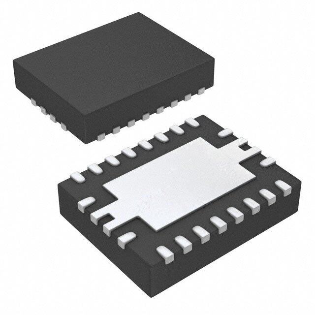
LTC4000-1 absoluTe MaxiMuM raTings (Note 1) IN, CLN, IID, CSP, CSN, BAT .......................–0.3V to 62V IBMON ..................................–0.3V to Min (V , V ) BIAS CSP IN-CLN, CSP-CSN ............................................–1V to 1V ITH ...............................................................–0.3V to 6V OFB, BFB, FBG ...........................................–0.3V to 62V CHRG, FLT, RST ..........................................–0.3V to 62V FBG ............................................................–1mA to 2mA CHRG, FLT, RST ..........................................–1mA to 2mA IGATE ...........Max (V , V ) – 10V to Max (V , V ) Operating Junction Temperature Range IID CSP IID CSP BGATE .......Max (V , V ) – 10V to Max (V , V ) (Note 2) .................................................................125°C BAT CSN BAT CSN ENC, CX, NTC, VM ...................................–0.3V to V Lead Temperature (Soldering, 10 sec) BIAS IFB, CL, TMR, IIMON, CC .........................–0.3V to V SSOP Package ..................................................300°C BIAS BIAS .............................................–0.3V to Min (6V, V ) Storage Temperature Range ..................–65°C to 150°C IN pin conFiguraTion TOP VIEW TOP VIEW ENC 1 28 IFB GND IN CLN CC ITH IID IBMON 2 27 IIMON 28 27 26 25 24 23 CX 3 26 RST VM 1 22 IGATE CL 4 25 VM RST 2 21 OFB TMR 5 24 GND IIMON 3 20 CSP GND 6 23 IN IFB 4 29 19 CSN FLT 7 22 CLN ENC 5 GND 18 BGATE CHRG 8 21 CC IBMON 6 17 BAT BIAS 9 20 ITH CX 7 16 BFB NTC 10 19 IID CL 8 15 FBG FBG 11 18 IGATE 9 10 11 12 13 14 TMR GND FLT CHRG BIAS NTC BBAFBT 1123 1176 OCSFBP UFD PACKAGE BGATE 14 15 CSN 28-LEAD (4mm × 5mm) PLASTIC QFN TJMAX = 125°C, θJA = 43°C/W, θJC = 4°C/W GN PACKAGE EXPOSED PAD (PIN 29) IS GND, MUST BE SOLDERED TO PCB 28-LEAD PLASTIC SSOP TJMAX = 125°C, θJA = 80°C/W, θJC = 25°C/W orDer inForMaTion LEAD FREE FINISH TAPE AND REEL PART MARKING* PACKAGE DESCRIPTION TEMPERATURE RANGE LTC4000EUFD-1#PBF LTC4000EUFD-1#TRPBF 40001 28-Lead (4mm × 5mm) Plastic QFN –40°C to 125°C LTC4000IUFD-1#PBF LTC4000IUFD-1#TRPBF 40001 28-Lead (4mm × 5mm) Plastic QFN –40°C to 125°C LTC4000EGN-1#PBF LTC4000EGN-1#TRPBF LTC4000GN-1 28-Lead Plastic SSOP –40°C to 125°C LTC4000IGN-1#PBF LTC4000IGN-1#TRPBF LTC4000GN-1 28-Lead Plastic SSOP –40°C to 125°C Consult LTC Marketing for parts specified with wider operating temperature ranges. *The temperature grade is identified by a label on the shipping container. Consult LTC Marketing for information on non-standard lead based finish parts. For more information on lead free part marking, go to: http://www.linear.com/leadfree/ For more information on tape and reel specifications, go to: http://www.linear.com/tapeandreel/ 40001fa 2 For more information www.linear.com/LTC4001-1
LTC4000-1 elecTrical characTerisTics The l denotes the specifications which apply over the full operating junction temperature range, otherwise specifications are at T = 25°C. V = V = 3V to 60V unless otherwise noted (Notes 2, 3). A IN CLN SYMBOL PARAMETER CONDITIONS MIN TYP MAX UNITS V Input Supply Operating Range l 3 60 V IN I Input Quiescent Operating Current 0.4 mA IN I Battery Pin Operating Current V ≥ 3V, V = V ≥ V l 50 100 µA BAT IN CSN CSP BAT Battery Only Quiescent Current V = 0V, V = V ≤ V l 10 20 μA IN CSN CSP BAT Shutdown ENC Input Voltage Low l 0.4 V ENC Input Voltage High l 1.5 V ENC Pull-Up Current V = 0V –4 –2 –0.5 µA ENC ENC Open Circuit Voltage V = Open l 1.5 2.5 V ENC Voltage Regulation V Input Feedback Voltage l 0.985 1.000 1.010 V IFB_REG IFB Input Current V = 1.0V ± 0.1 µA IFB V Battery Feedback Voltage 1.133 1.136 1.139 V BFB_REG l 1.120 1.136 1.147 V BFB Input Current V = 1.2V ± 0.1 µA BFB V Output Feedback Voltage l 1.176 1.193 1.204 V OFB_REG OFB Input Current V = 1.2V ± 0.1 µA OFB R Ground Return Feedback Resistance l 100 400 Ω FBG V Rising Recharge Battery Threshold Voltage % of V l 96.9 97.6 98.3 % RECHRG(RISE) BFB_REG V Recharge Battery Threshold Voltage Hysteresis % of V 0.5 % RECHRG(HYS) BFB_REG V Instant-On Battery Voltage Threshold % of V l 82 86 90 % OUT(INST_ON) BFB_REG V Falling Low Battery Threshold Voltage % of V l 65 68 71 % LOBAT BFB_REG V Low Battery Threshold Voltage Hysteresis % of V 3 % LOBAT(HYS) BFB_REG Current Monitoring and Regulation Ratio of Monitored-Current Voltage to Sense V ≤ 50mV, V /V l 18.5 20 21 V/V IN,CLN IIMON IN,CLN Voltage V ≤ 50mV, V /V CSP,CSN IBMON CSP,CSN V Sense Voltage Offset V ≤ 50mV, V = 60V or OS CSP,CSN CSP V ≤ 50mV, V = 60V (Note 4) –300 300 µV IN,CLN IN CLN, CSP, CSN Common Mode Range (Note 4) l 3 60 V CLN Pin Current ±1 µA CSP Pin Current V = Open, V = 0V 90 μA IGATE IID CSN Pin Current V = Open, V = 0V 45 μA BGATE BAT I Pull-Up Current for the Charge Current Limit l –55 –50 –45 μA CL Programming Pin I Pull-Up Current for the Charge Current Limit V < V l –5.5 –5.0 –4.5 μA CL_TRKL BFB LOBAT Programming Pin in Trickle Charge Mode Input Current Monitor Resistance to GND 40 90 140 kΩ Charge Current Monitor Resistance to GND 40 90 140 kΩ A5 Error Amp Offset for the Charge Current V = 0.8V l –10 0 10 mV CL Loop (See Figure 1) Maximum Programmable Current Limit l 0.985 1.0 1.015 V Voltage Range 40001fa 3 For more information www.linear.com/LTC4001-1
LTC4000-1 elecTrical characTerisTics The l denotes the specifications which apply over the full operating junction temperature range, otherwise specifications are at T = 25°C. V = V = 3V to 60V unless otherwise noted (Notes 2, 3). A IN CLN SYMBOL PARAMETER CONDITIONS MIN TYP MAX UNITS Charge Termination CX Pin Pull-Up Current V = 0.1V l –5.5 –5.0 –4.5 µA CX V CX Comparator Offset Voltage, IBMON Falling V = 0.1V l 0.5 10 25 mV CX,IBMON(OS) CX V CX Comparator Hysteresis Voltage 5 mV CX,IBMON(HYS) TMR Pull-Up Current V = 0V –5.0 μA TMR TMR Pull-Down Current V = 2V 5.0 μA TMR TMR Pin Frequency C = 0.01μF 400 500 600 Hz TMR TMR Threshold for CX Termination l 2.1 2.5 V t Charge Termination Time C = 0.1μF l 2.3 2.9 3.5 h T TMR t /t Ratio of Charge Terminate Time to Bad Battery C = 0.1μF l 3.95 4 4.05 h/h T BB TMR Indicator Time V NTC Cold Threshold V Rising, % of V l 73 75 77 % NTC(COLD) NTC BIAS V NTC Hot Threshold V Falling, % of V l 33 35 37 % NTC(HOT) NTC BIAS V NTC Thresholds Hysteresis % of V 5 % NTC(HYS) BIAS V NTC Open Circuit Voltage % of V l 45 50 55 % NTC(OPEN) BIAS R NTC Open Circuit Input Resistance 300 kΩ NTC(OPEN) Voltage Monitoring and Open Drain Status Pins V VM Input Falling Threshold l 1.176 1.193 1.204 V VM(TH) V VM Input Hysteresis 40 mV VM(HYS) VM Input Current V = 1.2V ±0.1 µA VM I Open Drain Status Pins Leakage Current V = 60V ±1 µA RST,CHRG,FLT(LKG) PIN V Open Drain Status Pins Voltage Output Low I = 1mA l 0.4 V RST,CHRG,FLT(VOL) PIN Input PowerPath Control Input PowerPath Forward Regulation Voltage V , 3V ≤ V ≤ 60V l 0.1 8 20 mV IID,CSP CSP Input PowerPath Fast Reverse Turn-Off V , 3V ≤ V ≤ 60V, l –90 –50 –20 mV IID,CSP CSP Threshold Voltage V = V – 2.5V, IGATE CSP ∆I /∆ V ≥ 100μA/mV IGATE IID,CSP Input PowerPath Fast Forward Turn-On V , 3V ≤ V ≤ 60V, l 40 80 130 mV IID,CSP CSP Threshold Voltage V = V – 1.5V, IGATE IID ∆I /∆ V ≥ 100μA/mV IGATE IID,CSP Input Gate Turn-Off Current V = V , V = V – 1.5V –0.3 μA IID CSP IGATE CSP Input Gate Turn-On Current V = V – 20mV, 0.3 μA CSP IID V = V – 1.5V IGATE IID I Input Gate Fast Turn-Off Current V = V + 0.1V, –0.5 mA IGATE(FASTOFF) CSP IID V = V – 5V IGATE CSP I Input Gate Fast Turn-On Current V = V – 0.2V, 0.7 mA IGATE(FASTON) CSP IID V = V – 1.5V IGATE IID V Input Gate Clamp Voltage I = 2µA, V = 12V to 60V, l 13 15 V IGATE(ON) IGATE IID V = V – 0.5V, Measure CSP IID V – V IID IGATE Input Gate Off Voltage I = – 2μA, V = 3V to 59.5V, l 0.45 0.7 V IGATE IID V = V + 0.5V, Measure CSP IID V – V CSP IGATE 40001fa 4 For more information www.linear.com/LTC4001-1
LTC4000-1 elecTrical characTerisTics The l denotes the specifications which apply over the full operating junction temperature range, otherwise specifications are at T = 25°C. V = V = 3V to 60V unless otherwise noted (Notes 2, 3). A IN CLN SYMBOL PARAMETER CONDITIONS MIN TYP MAX UNITS Battery PowerPath Control Battery Discharge PowerPath Forward V , 2.8V ≤ V ≤ 60V l 0.1 8 20 mV BAT,CSN BAT Regulation Voltage Battery PowerPath Fast Reverse Turn-Off V , 2.8V ≤ V ≤ 60V, Not l –90 –50 –20 mV BAT,CSN BAT Threshold Voltage Charging, V = V – 2.5V, BGATE CSN ∆I /∆V ≥ 100μA/mV BGATE BAT,CSN Battery PowerPath Fast Forward Turn-On V , 2.8V ≤ V ≤ 60V, l 40 80 130 mV BAT,CSN CSN Threshold Voltage V = V – 1.5V, BGATE BAT ∆I /∆ V ≥ 100μA/mV BGATE BAT,CSN Battery Gate Turn-Off Current V = V – 1.5V, V ≥ V , –0.3 μA BGATE CSN CSN BAT V < V and Charging OFB OUT(INST_ON) in Progress, or V = V and Not CSN BAT Charging Battery Gate Turn-On Current V = V – 1.5V, V ≥ V , 0.3 μA BGATE BAT CSN BAT V > V and Charging in OFB OUT(INST_ON) Progress, or V = V – 20mV CSN BAT I Battery Gate Fast Turn-Off Current V = V + 0.1V and Not –0.5 mA BGATE(FASTOFF) CSN BAT Charging, V = V – 5V BGATE CSN I Battery Gate Fast Turn-On Current V = V – 0.2V, 0.7 mA BGATE(FASTON) CSN BAT V = V – 1.5V BGATE BAT V Battery Gate Clamp Voltage I = 2μA, V = 12V to 60V, l 13 15 V BGATE(ON) BGATE BAT V = V – 0.5V, Measure CSN BAT V – V BAT BGATE Battery Gate Off Voltage I = – 2μA, V = 2.8V to 59.5V, l 0.45 0.7 V BGATE BAT V = V + 0.5V and not Charging, CSN BAT Measure V – V CSN BGATE BIAS Regulator Output and Control Pins V BIAS Output Voltage No Load l 2.4 2.9 3.5 V BIAS ∆V BIAS Output Voltage Load Regulation I = – 0.5mA –0.5 –10 % BIAS BIAS BIAS Output Short-Circuit Current V = 0V –20 mA BIAS Transconductance of Error Amp CC = 1V 0.5 mA/V Open Loop DC Voltage Gain of Error Amp CC = Open 80 dB I Pull-Up Current on the ITH Pin V = 0V, CC = 0V –6 –5 –4 μA ITH(PULL_UP) ITH I Pull-Down Current on the ITH Pin V = 0.4V, CC = Open l 0.5 1 mA ITH(PULL_DOWN) ITH Open Loop DC Voltage Gain of ITH Driver ITH = Open 60 dB Note 1: Stresses beyond those listed under Absolute Maximum Ratings these specifications is determined by specific operating conditions in may cause permanent damage to the device. Exposure to any Absolute conjunction with board layout, the rated package thermal impedance Maximum Rating condition for extended periods may affect device and other environmental factors. The junction temperature (T , in °C) is J reliability and lifetime. calculated from the ambient temperature (T , in °C) and power dissipation A Note 2: The LTC4000-1 is tested under conditions such that TJ ≈ TA. (PD, in Watts) according to the following formula: The LTC4000E-1 is guaranteed to meet specifications from 0°C to 85°C TJ = TA + (PD • θJA), where θJA (in °C/W) is the package thermal junction temperature. Specifications over the –40°C to 125°C operating impedance. junction temperature range are assured by design, characterization Note 3: All currents into pins are positive; all voltages are referenced to and correlation with statistical process controls. The LTC4000I-1 is GND unless otherwise noted. guaranteed over the full –40°C to 125°C operating junction temperature Note 4: These parameters are guaranteed by design and are not 100% range. Note that the maximum ambient temperature consistent with tested. 40001fa 5 For more information www.linear.com/LTC4001-1
LTC4000-1 Typical perForMance characTerisTics Input Voltage Regulation Feedback, Input Quiescent Current and Battery Float Voltage Feedback, Output Battery Quiescent Current Over Battery Only Quiescent Current Voltage Regulation Feedback and VM Temperature Over Temperature Falling Threshold Over Temperature 1.0 100 1.20 VIN = VBAT = 15V VCSN = 15.5V IIN 10 VBAT = 60V 11..1186 VVM(TH) VOFB_REG mA) A) 1 VBAT = 15V GE (V) 11..1124 VBFB_REG I/I (INBAT 0.1 IBAT I (µBAT 0.1 VBAT = 3V PIN VOLTA 111...000086 1.04 0.01 1.02 VIFB_REG 1.00 0 0.001 –60–40–20 0 20 40 60 80 100120140 –60–40–20 0 20 40 60 80 100120140 –60–40–20 0 20 40 60 80 100120140 TEMPERATURE (°C) TEMPERATURE (°C) TEMPERATURE (°C) 40001 G01 40001 G02 40001 G03 Battery Thresholds: Rising Recharge, Instant-On Regulation and Falling Low Battery As a Percentage of Battery CL Pull-Up Current Over Maximum Programmable Current Float Feedback Over Temperature Temperature Limit Voltage Over Temperature 100 –45.0 1.015 95 VRECHRG(RISE) 1.010 %) 90 –47.5 (REG 85 1.005 NT OF VBFB_ 7850 VOUT(INST_ON) I(µA)CL –50.0 V(V)IBMON 1.000 E 0.995 C R PE 70 VLOBAT –52.5 0.990 65 60 –55.0 0.985 –60–40–20 0 20 40 60 80 100120140 –60–40–20 0 20 40 60 80 100120140 –60–40–20 0 20 40 60 80 100120140 TEMPERATURE (°C) TEMPERATURE (°C) TEMPERATURE (°C) 40001 G04 40001 G05 40001 G06 Current Sense Offset Voltage Current Sense Offset Voltage Over CX Comparator Offset Voltage with Over Temperature Common Mode Voltage Range V Falling Over Temperature IBMON 300 300 20 VMAX(IN,CLN) = VMAX(CSP, CSN) = 15V 19 18 200 200 17 16 15 (µV)S 1000 VOS(CSP, CSN) (µV)S 1000 VOS(CSP, CSN) (mV)MON 11114321 O O B V–100 VOS(IN, CSN) V–100 VOS(IN, CSN) VCX,I 190 8 7 –200 –200 6 5 4 –300 –300 3 –60–40–20 0 20 40 60 80 100120140 03 10 20 30 40 50 60 –60–40–20 0 20 40 60 80 100120140 TEMPERATURE (°C) VMAX(IN, CLN)/VMAX(CSP, CSN) (V) TEMPERATURE (°C) 40001 G07 40001 G08 40001 G09 40001fa 6 For more information www.linear.com/LTC4001-1
LTC4000-1 Typical perForMance characTerisTics Charge Termination Time with 0.1µF NTC Thresholds Over PowerPath Forward Voltage Timer Capacitor Over Temperature Temperature Regulation Over Temperature 3.5 80 VNTC(COLD) 14 75 3.3 70 12 T(h)T 32..19 ENT OF V (%)BIAS 65655500 VNTC(OPEN) /V (mV)SPBAT,CSN 1608 VIID = VVBIIADT ==V VI1IDB5A V=T V=B 6A0TV = 3V 2.7 PERC 45 VNTC(HOT) VIID,C 4 40 2.5 2 35 2.3 30 0 –60–40–20 0 20 40 60 80 100120140 –60–40–20 0 20 40 60 80 100120140 –60–40–20 0 20 40 60 80 100120140 TEMPERATURE (°C) TEMPERATURE (°C) TEMPERATURE (°C) 40001 G10 40001 G11 40001 G12 PowerPath Fast Off, Fast On and Forward Regulation Over PowerPath Turn-On Gate Clamp PowerPath Turn-Off Gate Voltage Temperature Voltage Over Temperature Over Temperature 15.0 600 120 VIID = VBAT = 15V VIID = VBAT = 15V VCSP = VCSN = 15V 14.5 550 90 V/V (mV)IID,CSPBAT,CSN–6330000 V/V (V)IGATE(ON)BGATE(ON)1111123432.....55000 V/V (mV)CSP,IGATECSN,BGATE 345435500000000 –60 11.5 250 –90 11.0 200 –60–40–20 0 20 40 60 80 100120140 –60–40–20 0 20 40 60 80 100120140 –60–40–20 0 20 40 60 80 100120140 TEMPERATURE (°C) TEMPERATURE (°C) TEMPERATURE (°C) 40001 G13 40001 G14 40001 G15 BIAS Voltage at 0.5mA Load Over I Pull-Down Current Over I Pull-Down Current TH TH Temperature Temperature vs V ITH 3.2 1.5 2.5 VITH = 0.4V 1.4 3.1 1.3 2.0 3.0 VIN = 60V A) 1.2 A) m m V (V)BIAS 22..89 VIN = 3VVIN = 15V (ULL-DOWN) 110...019 (ULL-DOWN) 11..50 P P H( H( 2.7 IIT 0.8 IIT 0.7 0.5 2.6 0.6 2.5 0.5 0 –60–40–20 0 20 40 60 80 100120140 –60–40–20 0 20 40 60 80 100120140 0 0.1 0.2 0.3 0.4 0.5 0.6 0.7 0.8 0.9 1 TEMPERATURE (°C) TEMPERATURE (°C) VITH (V) 40001 G16 40001 G17 40001 G18 40001fa 7 For more information www.linear.com/LTC4001-1
LTC4000-1 pin FuncTions (QFN/SSOP) VM (Pin 1/Pin 25): Voltage Monitor Input. High impedance ENC (Pin 5/Pin 1): Enable Charging Pin. High impedance input to an accurate comparator with a 1.193V threshold digital input pin. Pull this pin above 1.5V to enable charg- (typical). This pin controls the state of the RST output ing and below 0.5V to disable charging. Leaving this pin pin. Connect a resistor divider (R , R ) between the open causes the internal 2µA pull-up current to pull the VM1 VM2 monitored voltage and GND, with the center tap point con- pin to 2.5V (typical). nected to this pin. The falling threshold of the monitored IBMON (Pin 6/Pin 2): Battery Charge Current Monitor. The voltage is calculated as follows: voltage on this pin is 20 times (typical) the sense voltage R +R (V ) across the battery current sense resistor (R ), V = VM1 VM2 •1.193V CSP,CSN CS VM_RST therefore providing a voltage proportional to the battery R VM2 charge current. Connect an appropriate capacitor to this where R is the bottom resistor between the VM pin VM2 pin to obtain a voltage representation of the time-average and GND. Tie to the BIAS pin if voltage monitoring func- battery charge current. Short this pin to GND to disable tion is not used. charge current limit feature. RST (Pin 2/Pin 26): High Voltage Open Drain Reset Output. CX (Pin 7/Pin 3): Charge Current Termination Pro- When the voltage at the VM pin is below 1.193V, this status gramming. Connect the charge current termination pro- pin is pulled low. When driven low, this pin can disable gramming resistor (R ) to this pin. This pin is a high CX a DC/DC converter when connected to the converter’s impedance input to a comparator and sources 5μA of enable pin. This pin can also drive an LED to provide a current. When the voltage on this pin is greater than the visual status indicator of a monitored voltage. Short this charge current monitor voltage (V ), the CHRG pin IBMON pin to GND when not used. turns high impedance indicating that the CX threshold is IIMON (Pin 3/Pin 27): Input Current Monitor. The voltage reached. When this occurs, the charge current is imme- on this pin is 20 times (typical) the sense voltage (V ) diately terminated if the TMR pin is shorted to the BIAS IN,CLN across the input current sense resistor(R ), therefore pin, otherwise charging continues until the charge termi- IS providing a voltage proportional to the input current. nation timer expires. The charge current termination value Connect an appropriate capacitor to this pin to obtain a is determined using the following formula: voltage representation of the time-average input current. ( ) 0.25µA•R −0.5mV Leave this pin open when input current monitoring func- CX I = C/X tion is not needed. R CS IFB (Pin 4/Pin 28): Input Voltage Feedback Pin. This pin is Where R is the sense resistor connected to the CSP CS a high impedance input pin used to sense the input voltage and the CSN pins. Note that if R = R ≤ 19.1kΩ, where CX CL level. In regulation, the input voltage loop sets the voltage R is the charge current programming resistor, then the CL on this feedback pin to 1.000V. When the input feedback charge current termination value is one tenth the full charge voltage drops below 1.000V, the ITH pin is pulled down current, more familiarly known as C/10. Short this pin to to reduce the load on the input source. Connect this pin GND to disable CX termination. to the center node of a resistor divider between the IN pin and GND to set the input voltage regulation level. This CL (Pin 8/Pin 4): Charge Current Limit Programming. Con- regulation level can then be obtained as follows: nect the charge current programming resistor (RCL) to this pin. This pin sources 50µA of current. The regulation loop R V = OFB1 +1 •1.000V compares the voltage on this pin with the charge current IN_REG R monitor voltage (V ), and drives the ITH pin accord- OFB2 IBMON ingly to ensure that the programmed charge current limit If the input voltage regulation feature is not used, connect the IFB pin to the BIAS pin. 40001fa 8 For more information www.linear.com/LTC4001-1
LTC4000-1 pin FuncTions (QFN/SSOP) is not exceeded. The charge current limit is determined if the battery temperature is safe for charging. The charge using the following formula: current and charge timer are suspended if the thermistor indicates a temperature that is unsafe for charging. Once the R I =2.5µA• CL temperature returns to the safe region, charging resumes. CLIM R Leave the pin open or connected to a capacitor to disable CS the temperature qualified charging function. Where R is the sense resistor connected to the CSP CS FBG (Pin 15/Pin 11): Feedback Ground Pin. This is the and the CSN pins. Leave the pin open for the maximum ground return pin for the resistor dividers connected to charge current limit of 50mV/R . CS the BFB and OFB pins. As soon as the voltage at IN is valid TMR (Pin 9/Pin 5): Charge Timer. Attach 1nF of external (>3V typical), this pin has a 100Ω resistance to GND. When capacitance (CTMR) to GND for each 104 seconds of charge the voltage at IN is not valid, this pin is disconnected from termination time and 26 seconds of bad battery indicator GND to ensure that the resistor dividers connected to the time. Short to GND to prevent bad battery indicator time BFB and OFB pins do not continue to drain the battery and charge termination time from expiring – allowing a when the battery is the only available power source. continuous trickle charge and top off float voltage regula- BFB (Pin 16/Pin 12): Battery Feedback Voltage Pin. This tion charge. Short to BIAS to disable bad battery detect pin is a high impedance input pin used to sense the battery and enable C/X charging termination. voltage level. In regulation, the battery float voltage loop GND (Pins 10, 28, 29/Pins 6, 24): Device Ground Pins. sets the voltage on this pin to 1.136V (typical). Connect Connect the ground pins to a suitable PCB copper ground this pin to the center node of a resistor divider between plane for proper electrical operation. The QFN package the BAT pin and the FBG pin to set the battery float voltage. exposed pad must be soldered to PCB ground for rated The battery float voltage can then be obtained as follows: thermal performance. R +R V = BFB2 BFB1 •1.136V FLT, CHRG (Pin 11, Pin 12/Pin 7, Pin 8): Charge Status FLOAT R BFB2 Indicator Pins. These pins are high voltage open drain pull down pins. The FLT pin pulls down when there is an under BAT (Pin 17/Pin 13): Battery Pack Connection. Connect or over temperature condition during charging or when the battery to this pin. This pin is the anode of the battery the voltage on the BFB pin stays below the low battery ideal diode driver (the cathode is the CSN pin). threshold during charging for a period longer than the bad BGATE (Pin 18/Pin 14): External Battery PMOS Gate Drive battery indicator time. The CHRG pin pulls down during Output. When not charging, the BGATE pin drives the a charging cycle. Please refer to the application informa- external PMOS to behave as an ideal diode from the BAT tion section for details on specific modes indicated by the pin (anode) to the CSN pin (cathode). This allows efficient combination of the states of these two pins. Pull up each delivery of any required additional power from the battery of these pins with an LED in series with a resistor to a to the downstream system connected to the CSN pin. voltage source to provide a visual status indicator. Short these pins to GND when not used. When charging a heavily discharged battery, the BGATE pin is regulated to set the output feedback voltage (OFB BIAS (Pin 13/Pin 9): 2.9V Regulator Output. Connect a pin) to 86% of the battery float voltage (0.974V typical). capacitor of at least 470nF to bypass this 2.9V regulated This allows the instant-on feature, providing an immediate voltage output. Use this pin to bias the resistor divider to valid voltage level at the output when the LTC4000-1 is set up the voltage at the NTC pin. charging a heavily discharged battery. Once the voltage NTC (Pin 14/Pin 10): Thermistor Input. Connect a ther- on the OFB pin is above the 0.974V typical value, then the mistor from NTC to GND, and a corresponding resistor BGATE pin is driven low to ensure an efficient charging from BIAS to NTC. The voltage level on this pin determines path from the CSN pin to the BAT pin. 40001fa 9 For more information www.linear.com/LTC4001-1
LTC4000-1 pin FuncTions (QFN/SSOP) CSN (Pin 19/Pin 15): Charge Current Sense Negative Input (3V to 60V). To ensure that the input PMOS is turned off and Battery Ideal Diode Cathode. Connect a sense resistor when the IN pin voltage is not within its operating range, between this pin and the CSP pin. The LTC4000-1 senses connect a 10M resistor from this pin to the CSP pin. the voltage across this sense resistor and regulates it to a IID (Pin 23/Pin 19): Input Ideal Diode Anode. This pin is voltage equal to 1/20th (typical) of the voltage set at the the anode of the input ideal diode driver (the cathode is CL pin. The maximum regulated sense voltage is 50mV. the CSP pin). The CSN pin is also the cathode input of the battery ideal diode driver (the anode input is the BAT pin). Tie this pin ITH (Pin 24/Pin 20): High Impedance Control Voltage Pin. to the CSP pin if no charge current limit is desired. Refer to When any of the regulation loops (input voltage, charge the Applications Information section for complete details. current, battery float voltage or the output voltage) indicate that its limit is reached, the ITH pin will sink current (up to CSP (Pin 20/Pin 16): Charge Current Sense Positive Input 1mA) to regulate that particular loop at the limit. In many and Input Ideal Diode Cathode. Connect a sense resis- applications, this ITH pin is connected to the control/ tor between this pin and the CSN pin for charge current compensation node of a DC/DC converter. Without any sensing and regulation. This input should be tied to CSN external pull-up, the operating voltage range on this pin to disable the charge current regulation function. This is GND to 2.5V. With an external pull-up, the voltage on pin is also the cathode of the input ideal diode driver (the this pin can be pulled up to 6V. Note that the impedance anode is the IID pin). connected to this pin affects the overall loop gain. For OFB (Pin 21/Pin 17): Output Feedback Voltage Pin. This details, refer to the Applications Information section. pin is a high impedance input pin used to sense the output CC (Pin 25/Pin 21): Converter Compensation Pin. Connect voltage level. In regulation, the output voltage loop sets the an R-C network from this pin to the ITH pin to provide a voltage on this feedback pin to 1.193V. Connect this pin suitable loop compensation for the converter used. Refer to the center node of a resistor divider between the CSP to the Applications Information section for discussion and pin and the FBG pin to set the output voltage when battery procedure on choosing an appropriate R-C network for a charging is terminated and all the output load current is particular DC/DC converter. provided from the input. The output voltage can then be obtained as follows: CLN (Pin 26/Pin 22): Input Current Sense Negative Input. Connect a sense resistor between this pin and the IN pin. The R +R V = OFB2 OFB1 •1.193V LTC4000-1 senses the voltage across this sense resistor OUT R OFB2 and sets the voltage on the IIMON pin equal to 20 times this voltage. Tie this pin to the IN pin if the input current When charging a heavily discharged battery (such that V OFB monitoring feature is not used. Refer to the Applications < V ), the battery PowerPath PMOS connected OUT(INST_ON) Information section for complete details. to BGATE is regulated to set the voltage on this feedback pin to 0.974V (approximately 86% of the battery float IN (Pin 27/Pin 23): Input Supply Voltage: 3V to 60V. voltage). The instant-on output voltage is then as follows: Supplies power to the internal circuitry and the BIAS pin. Connect the power source to the downstream system and R +R V = OFB2 OFB1 •0.974V the battery charger to this pin. This pin is also the positive OUT(INST_ON) R sense pin for the input current monitor. Connect a sense OFB2 resistor between this pin and the CLN pin. Tie this pin to IGATE (Pin 22/Pin 18): Input PMOS Gate Drive Output. The CLN if the input current monitoring feature is not used. A IGATE pin drives the external PMOS to behave as an ideal local 0.1µF bypass capacitor to ground is recommended diode from the IID pin (anode) to the CSP pin (cathode) on this pin. when the voltage at the IN pin is within its operating range 40001fa 10 For more information www.linear.com/LTC4001-1
LTC4000-1 block DiagraM RIS OUT IN DC/DC CONVERTER SYSTEM CCLN CIID 10M CL LOAD CIN RC CC CIBMON IN CLN RST ITH CC IID IGATE IBMON RVM1 VM CSP CP1 – + RVM2 1.193V + 8mV +– 60k gm = 0.33Am9 – CSN RCS + – A8 A1 gm = 0.33m A2 LINEAR GATE DRIVER BGATE +– 8mV AND DIINOPDUET D IDREIVAELR gm A11 VCOLLATMAGPE IIMON ENABLE 0.974V CHARGING CIIMON 60k BATTERY IDEAL DIODE A10 ITH AND CC DRIVER AND INSTANT-ON DRIVER RIFB1 IFB A4 gm– BIAS ROFB1 RIFB2 1V –+gm Ag5m–+ 1V 55µ0AµA/CL – IN A7+ OFB OFB RCL gm– 1.193V LDO, RBEGF, REF A6+ BFB CP6 – 0.771V CBIAS BIAS gm– 1.136V ROFB2 + BFB RBFB1 CP5 + NTC + CP4 RBFB2 TOO COLD – 1.109V – FBG NTC FAULT LOGIC + CP3 CP2 BAT – TOO HOT BIAS CBAT – + + 5µA – 10mV RNTC –+ BIAS CX 2µA BATTERY PACK TMR CTMR RCX OSCILLATOR GND ENC CHRG FLT 40001 BD R3 Figure 1. LTC4000-1 Functional Block Diagram 40001fa 11 For more information www.linear.com/LTC4001-1
LTC4000-1 operaTion Overview the battery float voltage loop is disabled. Charging is enabled when the ENC pin is left floating or pulled high (≥1.5V) The LTC4000-1 is designed to simplify the conversion of any externally compensated DC/DC converter into a high The LTC4000-1 offers several user configurable battery performance battery charger with PowerPath control. It charge termination schemes. The TMR pin can be config- only requires the DC/DC converter to have a control or ured for either C/X termination, charge timer termination or external-compensation pin (usually named VC or ITH) no termination. After a particular charge cycle terminates, whose voltage level varies in a positive monotonic way the LTC4000-1 features an automatic recharge cycle if the with its output. The output variable can be either output battery voltage drops below 97.6% of the programmed voltage or output current. For the following discussion, float voltage. refer to the Block Diagram in Figure 1. Trickle charge mode drops the charge current to one The LTC4000-1 includes four different regulation loops: tenth of the normal charge current (programmed using a input voltage, charge current, battery float voltage and resistor from the CL pin to GND) when charging into an output voltage (A4-A7). Whichever loop requires the low- over discharged or dead battery. When trickle charging, est voltage on the ITH pin for its regulation controls the a capacitor on the TMR pin can be used to program a external DC/DC converter. time out period. When this bad battery timer expires and the battery voltage fails to charge above the low battery The input voltage regulation loop ensures that the input threshold (V ), the LTC4000-1 will terminate charging voltage level does not drop below the programmed level. LOBAT and indicate a bad battery condition through the status The charge current regulation loop ensures that the pro- pins (FLT and CHRG). grammed battery charge current limit (using a resistor at CL) is not exceeded. The float voltage regulation loop The LTC4000-1 also includes an NTC pin, which provides ensures that the programmed battery stack voltage (us- temperature qualified charging when connected to an NTC ing a resistor divider from BAT to FBG via BFB) is not thermistor thermally coupled to the battery pack. To enable exceeded. The output voltage regulation loop ensures that this feature, connect the thermistor between the NTC and the programmed system output voltage (using a resistor the GND pins, and a corresponding resistor from the BIAS divider from CSP to FBG via OFB) is not exceeded. The pin to the NTC pin. The LTC4000-1 also provides a charg- LTC4000-1 also provides monitoring pins for the input ing status indicator through the FLT and the CHRG pins. current and charge current at the IIMON and IBMON pins Aside from biasing the thermistor-resistor network, the respectively. BIAS pin can also be used for a convenient pull up voltage. The LTC4000-1 features an ideal diode controller at the This pin is the output of a low dropout voltage regulator input from the IID pin to the CSP pin and a PowerPath that is capable of providing up to 0.5mA of current. The controller at the output from the BAT pin to the CSN pin. regulated voltage on the BIAS pin is available as soon as The output PowerPath controller behaves as an ideal the IN pin is within its operating range (≥3V). diode controller when not charging. When charging, the output PowerPath controller has two modes of operation. Input Ideal Diode If V is greater than V , BGATE is driven low. OFB OUT(INST_ON) The input ideal diode feature provides low loss conduction When V is less than V , a linear regulator OFB OUT(INST_ON) and reverse blocking from the IID pin to the CSP pin. This implements the instant-on feature. This feature provides reverse blocking prevents reverse current from the output regulation of the BGATE pin so that a valid voltage level is (CSP pin) to the input (IID pin) which causes unneces- immediately available at the output when the LTC4000-1 is sary drain on the battery and in some cases may result charging an over-discharged, dead or short faulted battery. in unexpected DC/DC converter behavior. The state of the ENC pin determines whether charging is The ideal diode behavior is achieved by controlling an enabled. When ENC is grounded, charging is disabled and external PMOS connected to the IID pin (drain) and the 40001fa 12 For more information www.linear.com/LTC4001-1
LTC4000-1 operaTion CSP pin (source). The controller (A1) regulates the external When a battery charge cycle begins, the battery charger PMOS by driving the gate of the PMOS device such that the first determines if the battery is over-discharged. If the voltage drop across IID and CSP is 8mV (typical). When battery feedback voltage is below V , an automatic LOBAT the external PMOS ability to deliver a particular current trickle charge feature uses the charge current regulation with an 8mV drop across its source and drain is exceeded, loop to set the battery charge current to 10% of the pro- the voltage at the gate clamps at VIGATE(ON) and the PMOS grammed full-scale value. If the TMR pin is connected behaves like a fixed value resistor (RDS(ON)). to a capacitor or open, the bad battery detection timer is enabled. When this bad battery detection timer expires Note that this input ideal diode function is only enabled and the battery voltage is still below V , the battery when the voltage at the IN pin is within its operating range LOBAT charger automatically terminates and indicates, via the (3V to 60V). To ensure that the external PMOS is turned FLT and CHRG pins, that the battery was unresponsive off when the voltage at the IN pin is not within is operating range, a 10M pull-up resistor between the IGATE and the to charge current. CSP pin is recommended. Once the battery voltage is above V , the charge current LOBAT regulation loop begins charging in full power constant- Input Voltage Regulation current mode. In this case, the programmed full charge One of the loops driving the ITH and CC pins is the input current is set with a resistor on the CL pin. voltage regulation loop (Figure 2). This loop prevents the Depending on available input power and external load input voltage from dropping below the programmed level. conditions, the battery charger may not be able to charge RIS at the full programmed rate. The external load is always IN DC/DC INPUT prioritized over the battery charge current. The input volt- CIN C(OCPLTNIONAL) age programming is always observed, and only additional power is available to charge the battery. When system IN CLN LTC4000-1 loads are light, battery charge current is maximized. CC RIFB1 CC Once the float voltage is achieved, the battery float volt- IFB – RIFB2 1V +A4 –+ ITH RC TO DC/DC areggeu rlaetgiounla ltoioonp laonodp i ntaitkiaetse so cvoenr sftraonmt vtohleta cghea crhgaer gciunrgre. nInt constant voltage charging, charge current slowly declines. 40001 FO2 Figure 2. Input Voltage Regulation Loop Charge termination can be configured with the TMR pin When the input source is high impedance, the input volt- in several ways. If the TMR pin is tied to the BIAS pin, age drops as the load current increases. In that case there C/X termination is selected. In this case, charging is exists a voltage level at which the available power from terminated when constant voltage charging reduces the the input is maximum. For example, solar panels often charge current to the C/X level programmed at the CX specify V , corresponding to the panel voltage at which pin. Connecting a capacitor to the TMR pin selects the MP maximum power is achieved. With the LTC4000-1 input charge timer termination and a charge termination timer voltage regulation, this maximum power voltage level can is started at the beginning of constant voltage charging. be programmed at the IFB pin. The input voltage regulation Charging terminates when the termination timer expires. loop regulates ITH to ensure that the input voltage level When continuous charging at the float voltage is desired, does not drop below this programmed level. tie the TMR pin to GND to disable termination. Upon charge termination, the PMOS connected to BGATE Battery Charger Overview behaves as an ideal diode from BAT to CSN. The diode In addition to the input voltage regulation loop, the function prevents charge current but provides current LTC4000-1 regulates charge current, battery voltage and to the system load as needed. If the system load can be output voltage. completely supplied from the input, the battery PMOS turns 40001fa 13 For more information www.linear.com/LTC4001-1
LTC4000-1 operaTion off. While terminated, if the input voltage loop is not in BAT LTC4000-1 CC regulation, the output voltage regulation loop takes over to RBFB1 CC ensure that the output voltage at CSP remains in control. BFB + – RC The output voltage regulation loop regulates the voltage RBFB2 FBG 1.136V –A6 + ITH TO DC/DC at the CSP pin such that the output feedback voltage at the OFB pin is 1.193V. 40001 FO4 If the system load requires more power than is available Figure 4. Battery Float Voltage Regulation Loop with FBG from the input, the battery ideal diode controller provides supplemental power from the battery. When the battery tor divider does not consume battery current when the voltage discharges below 97.1% of the float voltage battery is the only available power source. For V ≥ 3V, IN (VBFB < VRECHRG(FALL)), the automatic recharge feature the typical resistance from the FBG pin to GND is 100Ω. initiates a new charge cycle. Output Voltage Regulation Charge Current Regulation When charging terminates and the system load is com- The first loop involved in a normal charging cycle is the pletely supplied from the input, the PMOS connected to charge current regulation loop (Figure 3). This loop drives BGATE is turned off. In this scenario, the output voltage the ITH and CC pins. This loop ensures that the charge regulation loop takes over from the battery float voltage current sensed through the charge current sense resistor regulation loop (Figure 5). The output voltage regulation (R ) does not exceed the programmed full charge current. CS loop regulates the voltage at the CSP pin such that the output feedback voltage at the OFB pin is 1.193V. TO SYSTEM RIS CSP BAT PMOS CCSP CSP LTC4000-1 CC ROFB1 CC OFB + CSP CSN LTC4000-1 – RC ROFB2 1.193V – ITH TO DC/DC + – A9 FBG A7 + gm = 0.33m IBMON CC CIBMON 60k + CC (OPTIONAL) BIAS – – RC 40001 FO5 ITH 50µA AT NORMAL 1V – + TO DC/DC Figure 5. Output Voltage Regulation Loop with FBG 5µA AT TRICKLE A5 RCL CL Battery Instant-On and Ideal Diode 40001 FO3 Figure 3. Charge Current Regulation Loop The LTC4000-1 controls the external PMOS connected to the BGATE pin with a controller similar to the input ideal Battery Voltage Regulation diode controller driving the IGATE pin. When not charg- Once the float voltage is reached, the battery voltage regu- ing, the PMOS behaves as an ideal diode between the BAT lation loop takes over from the charge current regulation (anode) and the CSN (cathode) pins. The controller (A2) loop (Figure 4). regulates the external PMOS to achieve low loss conduc- tion by driving the gate of the PMOS device such that the The float voltage level is programmed using the feedback voltage drop from the BAT pin to the CSN pin is 8mV. resistor divider between the BAT pin and the FBG pin with When the ability to deliver a particular current with an 8mV the center node connected to the BFB pin. Note that the drop across the PMOS source and drain is exceeded, the ground return of the resistor divider is connected to the voltage at the gate clamps at V and the PMOS BGATE(ON) FBG pin. The FBG pin disconnects the resistor divider behaves like a fixed value resistor (R ). DS(ON) load when V < 3V to ensure that the float voltage resis- IN 40001fa 14 For more information www.linear.com/LTC4001-1
LTC4000-1 operaTion The ideal diode behavior allows the battery to provide cur- pauses until the thermistor indicates a return to a valid rent to the load when the input supply is in current limit temperature. or the DC/DC converter is slow to react to an immediate load increase at the output. In addition to the ideal diode Input UVLO and Voltage Monitoring behavior, BGATE also allows current to flow from the CSN The regulated voltage on the BIAS pin is available as soon pin to the BAT pin during charging. as V ≥ 3V. When V ≥ 3V, the FBG pin is pulled low to IN IN GND with a typical resistance of 100Ω and the rest of the There are two regions of operation when current is chip functionality is enabled. flowing from the CSN pin to the BAT pin. The first is when charging into a battery whose voltage is below When the IN pin is high impedance and a battery is con- the instant-on threshold (VOFB < VOUT(INST_ON)). In this nected to the BAT pin, the BGATE pin is pulled down with region of operation, the controller regulates the voltage a 2μA (typical) current source to hold the battery PMOS at the CSP pin to be approximately 86% of the final float gate voltage at V below V . This allows the BGATE(ON) BAT voltage level (V ). This feature provides a CSP battery to power the output. The total quiescent current OUT(INST_ON) voltage significantly higher than the battery voltage when consumed by LTC4000-1 from the battery when IN is not charging into a heavily discharged battery. This instant-on valid is typically ≤ 10µA. feature allows the LTC4000-1 to provide sufficient voltage When the IN pin is high impedance, the input ideal diode at the output (CSP pin), independent of the battery voltage. function for the external FET connected to the IGATE pin is The second region of operation is when the battery feedback disabled. To ensure that this FET is completely turned off voltage is greater than or equal to the instant-on threshold when the voltage at the IN pin is not within its operating (V ). In this region, the BGATE pin is driven range, connect a 10M pull-up resistor between the IGATE OUT(INST_ON) low and clamped at V to allow the PMOS to turn pin and the CSP pin. BGATE(ON) completely on, reducing any power dissipation due to the Besides the internal input UVLO, the LTC4000-1 also pro- charge current. vides voltage monitoring through the VM pin. The RST pin is pulled low when the voltage on the VM pin falls below Battery Temperature Qualified Charging 1.193V (typical). On the other hand, when the voltage on The battery temperature is measured by placing a nega- the VM pin rises above 1.233V (typical), the RST pin is tive temperature coefficient (NTC) thermistor close to the high impedance. battery pack. The comparators CP3 and CP4 implement One common use of this voltage monitoring feature is to the temperature detection as shown in the Block Diagram ensure that the converter is turned off when the voltage in Figure 1. The rising threshold of CP4 is set at 75% of at the input is below a certain level. In this case, connect V (cold threshold) and the falling threshold of CP3 is BIAS the RST pin to the DC/DC converter chip select or enable set at 35% of V (hot threshold). When the voltage at BIAS pin (see Figure 6). the NTC pin is above 75% of V or below 35% of V BIAS BIAS then the LTC4000-1 pauses any charge cycle in progress. RIS DC/DC IN IN CONVERTER When the voltage at the NTC pin returns to the range of EN 40% to 70% of V , charging resumes. BIAS RVM1 IN CLN RST When charging is paused, the external charging PMOS VM CP1 turns off and charge current drops to zero. If the LTC4000-1 – is charging in the constant voltage mode and the charge RVM2 termination timer is enabled, the timer pauses until the 1.193V + thermistor indicates a return to a valid temperature. If the LTC4000-1 40001 FO6 battery charger is in the trickle charge mode and the bad Figure 6. Input Voltage Monitoring with RST Connected to battery detection timer is enabled, the bad battery timer the EN Pin of the DC/DC Converter 40001fa 15 For more information www.linear.com/LTC4001-1
LTC4000-1 applicaTions inForMaTion Input Ideal Diode PMOS Selection pin to the CSP pin. Therefore, for a 10M R resistor IGATE and assuming a 10V V , the additional forward voltage The input external PMOS is selected based on the expected GSON regulation is ∆V REG = 20mV, and the total forward maximum current, power dissipation and reverse volt- IID,CSP voltage regulation is 28mV (typ). It is recommended to age drop. The PMOS must be able to withstand a gate to set the R such that this additional forward voltage source voltage greater than V (15V maximum) or IGATE IGATE(ON) regulation value does not exceed 40mV. the maximum regulated voltage at the IID pin, whichever is less. A few appropriate external PMOS for a number of Input Current Monitoring different requirements are shown at Table 1. The input current through the sense resistor is available Table 1. PMOS for monitoring through the IIMON pin. The voltage on R AT the IIMON pin varies with the current through the sense DS(ON) V = 10V MAX ID MAX VDS GS resistor as follows: PART NUMBER (Ω) (A) (V) MANUFACTURER SiA923EDJ 0.054 4.5 –20 Vishay VIIMON =20•IRIS •RIS =20•(VIN –VCLN) Si9407BDY 0.120 4.7 –60 Vishay If the input current is noisy, add a filter capacitor to the Si4401BDY 0.014 10.5 –40 Vishay CLN pin to reduce the AC content. For example, when us- Si4435DDY 0.024 11.4 –30 Vishay ing a buck DC/DC converter, the use of a C capacitor CLN SUD19P06-60 0.060 18.3 –60 Vishay is strongly recommended. Where the highest accuracy is Si7135DP 0.004 60 –30 Vishay important, pick the value of C such that the AC content CLN is less than or equal to 50% of the average voltage across Note that in general the larger the capacitance seen on the sense resistor. the IGATE pin, the slower the response of the ideal diode driver. The fast turn off and turn on current is limited to The voltage on the IIMON pin can be filtered further by –0.5mA and 0.7mA typical respectively (IIGATE(FASTOFF) and putting a capacitor on the pin (CIIMON). I ). If the driver can not react fast enough to a IGATE(FASTON) sudden increase in load current, most of the extra current Charge Current Limit Setting and Monitoring is delivered through the body diode of the external PMOS. The regulated full charge current is set according to the This increases the power dissipation momentarily. It is following formula: important to ensure that the PMOS is able to withstand this momentary increase in power dissipation. V R = CL CS The operation section also mentioned that an external 10M 20•I CLIM pull-up resistor is recommended between the IGATE pin where V is the voltage on the CL pin. The CL pin is CL and the CSP pin when the IN pin voltage is expected to internally pulled up with an accurate current source of be out of its operating range, at the same time that the 50µA. Therefore, an equivalent formula to obtain the external input ideal diode PMOS is expected to be com- charge current limit is: pletely turned off. Note that this additional pull-up resistor increases the forward voltage regulation of the ideal diode I •R R R = CLIM CS ⇒I = CL •2.5µA CL CLIM function (VIID,CSP) from the typical value of 8mV. 2.5µA RCS The increase in this forward voltage is calculated according The charge current through the sense resistor is available to the following formula: for monitoring through the IBMON pin. The voltage on ∆V REG = V • 20k/R the IBMON pin varies with the current through the sense IID,CSP GSON IGATE resistor as follows: where V is the source to gate voltage required to GSON achieve the desired ON resistance of the external PMOS V =20•I •R =20•(V –V ) IBMON RCS CS CSP CSN and R is the external pull-up resistor from the IGATE IGATE 40001fa 16 For more information www.linear.com/LTC4001-1
LTC4000-1 applicaTions inForMaTion The regulation voltage level at the IBMON pin is clamped Low Battery Trickle Charge Programming and Bad at 1V with an accurate internal reference. At 1V on the Battery Detection IBMON pin, the charge current limit is regulated to the When charging into an over-discharged or dead battery following value: (V < V ), the pull-up current at the CL pin is reduced BFB LOBAT 0.050V to 10% of the normal pull-up current. Therefore, the trickle I (A)= CLIM(MAX) R (Ω) charge current is set using the following formula: CS I •R R When this maximum charge current limit is desired, leave R = CLIM(TRKL) CS ⇒I =0.25µA• CL CL CLIM(TRKL) the CL pin open or set it to a voltage >1.05V such that 0.25µA R CS amplifier A5 can regulate the IBMON pin voltage accurately Therefore, when 50µA•R is less than 1V, the following to the internal reference of 1V. CL relation is true: When the output current waveform of the DC/DC converter I or the system load current is noisy, it is recommended that I = CLIM CLIM(TRKL) a capacitor is connected to the CSP pin (CCSP). This is to 10 reduce the AC content of the current through the sense Once the battery voltage rises above the low battery voltage resistor (R ). Where the highest accuracy is important, CS threshold, the charge current level rises from the trickle pick the value of C such that the AC content is less CSP charge current level to the full charge current level. than or equal to 50% of the average voltage across the sense resistor. Similar to the IIMON pin, the voltage on the The LTC4000-1 also features bad battery detection. This IBMON pin is filtered further by putting a capacitor on the detection is disabled if the TMR pin is grounded or tied pin (C ). This filter capacitor should not be arbitrarily to BIAS. However, when a capacitor is connected to the IBMON large as it will slow down the overall compensated charge TMR pin, a bad battery detection timer is started as soon current regulation loop. For details on the loop compensa- as trickle charging starts. If at the end of the bad battery tion, refer to the Compensation section. detection time the battery voltage is still lower than the low battery threshold, charging is terminated and the part Battery Float Voltage Programming indicates a bad battery condition by pulling the FLT pin low and leaving the CHRG pin high impedance. When the value of R is much larger than 100Ω, the final BFB1 float voltage is determined using the following formula: The bad battery detection time can be programmed ac- cording to the following formula: V RBFB1= FLOAT –1RBFB2 1.136V C (nF)=t (h)•138.5 TMR BADBAT When higher accuracy is important, a slightly more ac- Note that once a bad battery condition is detected, the curate final float voltage can be determined using the condition is latched. In order to re-enable charging, re- following formula: move the battery and connect a new battery whose voltage causes BFB to rise above the recharge battery threshold R +R R V = BFB1 BFB2 •1.136V – BFB1 •V (VRECHRG(RISE)). Alternatively toggle the ENC pin or remove FLOAT FBG R R and reapply power to IN. BFB2 BFB2 where VFBG is the voltage at the FBG pin during float C/X Detection, Charge Termination and Automatic voltage regulation, which accounts for all the current Recharge from all resistor dividers that are connected to this pin Once the constant voltage charging is reached, there are (R = 100Ω typical). FBG two ways in which charging can terminate. If the TMR pin is tied to BIAS, the battery charger terminates as soon as 40001fa 17 For more information www.linear.com/LTC4001-1
LTC4000-1 applicaTions inForMaTion the charge current drops to the level programmed by the V CX pin. The C/X current termination level is programmed R = OUT −1•R OFB1 OFB2 1.193 according to the following formula: As in the battery float voltage calculation, when higher (I •R )+0.5mV (0.25µA•R )−0.5mV R = C/X CS ⇒I = CX accuracy is important, a slightly more accurate output is CX C/X 0.25µA R CS determined using the following formula: where R is the charge current sense resistor connected CS R +R R between the CSP and the CSN pins. V = OFB1 OFB2 •1.193V– OFB1 •V OUT FBG R R When the voltage at BFB is higher than the recharge OFB2 OFB2 threshold (97.6% of float), the C/X comparator is enabled. where V is the voltage at the FBG pin during output FBG In order to ensure proper C/X termination coming out of voltage regulation, which accounts for all the current from a paused charging condition, connect a capacitor on the all resistor dividers that are connected to this pin. CX pin according to the following formula: Battery Instant-On and Ideal Diode External PMOS C = 100C CX BGATE Consideration where C is the total capacitance connected to the BGATE BGATE pin. The instant-on voltage level is determined using the fol- lowing formula: For example, a typical capacitance of 1nF requires a capaci- tor greater than 100nF connected to the CX pin to ensure V =ROFB1+ROFB2 •0.974V proper C/X termination behavior. OUT(INST_ON) R OFB2 If a capacitor is connected to the TMR pin, as soon as the Note that ROFB1 and ROFB2 are the same resistors that constant voltage charging is achieved, a charge termina- program the output voltage regulation level. Therefore, tion timer is started. When the charge termination timer the output voltage regulation level is always 122.5% of expires, the charge cycle terminates. The total charge the instant-on voltage level. termination time can be programmed according to the During instant-on operation, it is critical to consider the following formula: charging PMOS power dissipation. When the battery volt- CTMR(nF)=tTERMINATE(h)•34.6 age is below the low battery threshold (VLOBAT), the power dissipation in the PMOS can be calculated as follows: If the TMR pin is grounded, charging never terminates and P =[0.86•V –V ]•I the battery voltage is held at the float voltage. Note that TRKL FLOAT BAT CLIM(TRKL) regardless of which termination behavior is selected, the where I is the trickle charge current limit. CHRG and FLT pins will both assume a high impedance CLIM(TRKL) state as soon as the charge current falls below the pro- On the other hand, when the battery voltage is above the grammed C/X level. low battery threshold but still below the instant-on thresh- old, the power dissipation can be calculated as follows: After the charger terminates, the LTC4000-1 automatically restarts another charge cycle if the battery feedback voltage P =[0.86•V –V ]•I INST_ON FLOAT BAT CLIM drops below 97.1% of the programmed final float voltage where I is the full scale charge current limit. (V ). When charging restarts, the CHRG pin CLIM RECHRG(FALL) pulls low and the FLT pin remains high impedance. For example, when charging a 3-cell Lithium Ion battery with a programmed full charged current of 1A, the float Output Voltage Regulation Programming voltage is 12.6V, the bad battery voltage level is 8.55V and The output voltage regulation level is determined using the instant-on voltage level is 10.8V. During instant-on the following formula: operation and in the trickle charge mode, the worst case 40001fa 18 For more information www.linear.com/LTC4001-1
LTC4000-1 applicaTions inForMaTion maximum power dissipation in the PMOS is 1.08W. When R +R V = BFB1 BFB2 •1.136V the battery voltage is above the bad battery voltage level, FLOAT R then the worst case maximum power dissipation is 2.25W. BFB2 R +R When overheating of the charging PMOS is a concern, it is V = OFB1 OFB2 •1.193V OUT R recommended that the user add a temperature detection OFB2 circuit that pulls down on the NTC pin. This pauses charg- R +R V = OFB1 OFB2 •0.974V ing whenever the external PMOS temperature is too high. OUT(INST_ON) R OFB2 A sample circuit that performs this temperature detection function is shown in Figure 7. In the typical application, V is set higher than V OUT FLOAT to ensure that the battery is charged fully to its intended Similar to the input external PMOS, the charging external float voltage. On the other hand, V should not be PMOS must be able to withstand a gate to source voltage OUT programmed too high since V , the minimum greater than V (15V maximum) or the maximum OUT(INST_ON) BGATE(ON) voltage on CSP, depends on the same resistors R and regulated voltage at the CSP pin, whichever is less. Consider OFB1 R that set V . As noted before, this means that the the expected maximum current, power dissipation and OFB2 OUT output voltage regulation level is always 122.5% of the instant-on voltage drop when selecting this PMOS. The instant-on voltage. The higher the programmed value of PMOS suggestions in Table 1 are an appropriate starting V , the larger the operating region when the point depending on the application. OUT(INST_ON) charger PMOS is driven in the linear region where it is less efficient. Float Voltage, Output Voltage and Instant-On Voltage Dependencies If R and R are set to be equal to R and R OFB1 OFB2 BFB1 BFB2 respectively, then the output voltage is set at 105% of The formulas for setting the float voltage, output voltage the float voltage and the instant-on voltage is set at 86% and instant-on voltage are repeated here: of the float voltage. Figure 8 shows the range of possible TO SYSTEM VISHAY CURVE 2 NTC RESISTOR CSP THERMALLY COUPLED WITH CHARGING PMOS LTC4000-1 RCS RNTC2 CSN BGATE M2 R4 = RNTC2 AT 25°C BAT BIAS CBIAS 162k R3 NTC 2N7002L – RISING TEMPERATURE THRESHOLD Li-Ion + SET AT 90°C BATTERY PACK LTC1540 RNTC1 20k VOLTAGE HYSTERESIS CAN BE PROGRAMMED FOR TEMPERATURE HYSTERESIS 86mV ≈ 10°C 40001 F07 Figure 7. Charging PMOS Overtemperature Detection Circuit Protecting PMOS from Overheating 40001fa 19 For more information www.linear.com/LTC4001-1
LTC4000-1 applicaTions inForMaTion POSSIBLE POSSIBLE OUTPUT INSTANT-ON VOLTAGE RANGE VOLTAGE RANGE 105% MINIMUM PRACTICAL NOMINAL OUTPUT VOLTAGE OUTPUT VOLTAGE 100% 100% NOMINAL FLOAT VOLTAGE 100% 86% MINIMUM PRACTICAL NOMINAL INSTANT-ON VOLTAGE INSTANT-ON VOLTAGE 81.6% 75% 40001 F08 Figure 8. Possible Voltage Ranges for V and V in Ideal Scenario OUT OUT(INST_ON) output voltages that can be set for V and V In a simple application, R3 is a 1% resistor with a value OUT(INST_ON) OUT with respect to V to ensure the battery can be fully equal to the value of the chosen NTC thermistor at 25°C FLOAT charged in an ideal scenario. (R25). In this simple setup, the LTC4000-1 will pause charging when the resistance of the NTC thermistor Taking into account possible mismatches between the drops to 0.54 times the value of R25. For a Vishay resistor dividers as well as mismatches in the various Curve 2 thermistor, this corresponds to approximately regulation loops, V should not be programmed to OUT 41.5°C. As the temperature drops, the resistance of the be less than 105% of V to ensure that the battery FLOAT NTC thermistor rises. The LTC4000-1 is also designed can be fully charged. This automatically means that the to pause charging when the value of the NTC thermistor instant-on voltage level should not be programmed to be increases to three times the value of R25. For a Vishay less than 86% of V . FLOAT Curve 2 thermistor, this corresponds to approximately –1.5°C. With Vishay Curve 2 thermistor, the hot and cold Battery Temperature Qualified Charging comparators each have approximately 5°C of hysteresis To use the battery temperature qualified charging feature, to prevent oscillation about the trip point. connect an NTC thermistor, R , between the NTC pin NTC The hot and cold threshold can be adjusted by changing and the GND pin, and a bias resistor, R3, from the BIAS the value of R3. Instead of simply setting R3 to be equal to pin to the NTC pin (Figure 9). Thermistor manufacturer R25, R3 is set according to one of the following formulas: datasheets usually include either a temperature lookup table or a formula relating temperature to the resistor R at cold_threshold R3= NTC value at that corresponding temperature. 3 or BIAS LTC4000-1 R3 CBIAS R3=1.857•RNTC at hot_threshold NTC Notice that with only one degree of freedom (i.e. adjusting BAT the value of R3), the user can only use one of the formulas NTC RESISTOR RNTC above to set either the cold or hot threshold but not both. THERMALLY COUPLED WITH BATTERY PACK If the value of R3 is set to adjust the cold threshold, the 40001 F09 value of the NTC resistor at the hot threshold is then Figure 9. NTC Thermistor Connection 40001fa 20 For more information www.linear.com/LTC4001-1
LTC4000-1 applicaTions inForMaTion equal to 0.179 • R at cold_threshold. Similarly, if the if the user finds that a negative value is needed for R , NTC D value of R3 is set to adjust the hot threshold, the value the two temperature thresholds selected are too close to of the NTC resistor at the cold threshold is then equal to each other and a higher sensitivity thermistor is needed. 5.571 • R at cold_threshold. NTC For example, this method can be used to set the hot Note that changing the value of R3 to be larger than R25 and cold thresholds independently to 60°C and –5°C. will move both the hot and cold threshold lower and vice Using a Vishay Curve 2 thermistor whose nominal value versa. For example, using a Vishay Curve 2 thermistor at 25°C is 100k, the formula results in R3 = 130k and whose nominal value at 25°C is 100k, the user can set R = 41.2k for the closest 1% resistors values. D the cold temperature to be at 5°C by setting the value of To increase thermal sensitivity such that the valid charging R3 = 75k, which automatically then sets the hot threshold temperature band is much smaller than 40°C, it is pos- at approximately 50°C. sible to put a PTC (positive thermal coefficient) resistor It is possible to adjust the hot and cold threshold indepen- in series with R3 between the BIAS pin and the NTC pin. dently by introducing another resistor as a second degree This PTC resistor also needs to be thermally coupled with of freedom (Figure 10). The resistor R in effect reduces the battery. Note that this method increases the number of D the sensitivity of the resistance between the NTC pin and thermal sensing connections to the battery pack from one ground. Therefore, intuitively this resistor will move the hot wire to three wires. The exact value of the nominal PTC threshold to a hotter temperature and the cold threshold resistor required can be calculated using a similar method to a colder temperature. as described above, keeping in mind that the threshold at the NTC pin is always 75% and 35% of V . BIAS BIAS Leaving the NTC pin floating or connecting it to a capacitor LTC4000-1 R3 CBIAS disables all NTC functionality. NTC RD Battery Voltage Temperature Compensation BAT Some battery chemistries have charge voltage require- THERMANLTLCY R CEOSUISPTLOERD RNTC ments that vary with temperature. Lead-acid batteries in WITH BATTERY PACK 40001 F10 particular experience a significant change in charge volt- age requirements as temperature changes. For example, Figure 10. NTC Thermistor Connection with manufacturers of large lead-acid batteries recommend a Desensitizing Resistor R D float charge of 2.25V/cell at 25°C. This battery float voltage, however, has a temperature coefficient which is typically The value of R3 and R can now be set according to the D specified at –3.3mV/°C per cell. following formula: The LTC4000-1 employs a resistor feedback network to R at cold_threshold–R at hot_threshold R3= NTC NTC program the battery float voltage. manipulation of this 2.461 network makes for an efficient implementation of vari- R =0.219•R at cold_threshold– D NTC ous temperature compensation schemes of battery float 1.219•R at hot_threshold voltage. NTC A simple solution for tracking such a linear voltage de- Note the important caveat that this method can only be pendence on temperature is to use the LM234 3-terminal used to desensitize the thermal effect on the thermistor temperature sensor. This creates an easily programmable and hence push the hot and cold temperature thresholds linear temperature dependent characteristic. apart from each other. When using the formulas above, 40001fa 21 For more information www.linear.com/LTC4001-1
LTC4000-1 applicaTions inForMaTion 14.4 (TC = –19.8mV/°C and VFLOAT(25°C) = 13.5V) and RSET = 14.2 2.43k into the equation, we obtained the following values: 14.0 RBFB1 = 210k and RBFB2 = 13.0k. 13.8 (V)AT 13.6 3-Step Charging for Lead-Acid Battery VFLO 13.4 The LTC4000-1 naturally lends itself to charging ap- 13.2 plications requiring a constant current step followed by 13.0 constant voltage. Furthermore, the LTC4000-1 additional 12.8 features such as trickle charging, bad battery detection and C/X or timer termination makes it an excellent fit for 12.6 –10 0 10 20 30 40 50 60 Lithium based battery charging applications. Figure 13 TEMPERATURE (°C) 40001 F11 and Table 2 show the normal steps involved in Lithium Figure 11. Lead-Acid 6-Cell Float Charge Voltage vs battery charging. Temperature Using LM234 with the Feedback Network TRICKLE CONSTANT CONSTANT VOLTAGE TERMINATION CHARGE CURRENT BAT LM234 LTC4000-1 V+ RBFB1 R BATTERY VOLTAGE 210k RSET V– 2.43k BFB RBFB2 6-CELL 13.0k LEAD-ACID FBG BATTERY 40001 F12 CHARGE CURRENT Figure 12. Battery Voltage Temperature Compensation Circuit CHARGE TIME 40001 F13 Figure 13. Li-Ion Typical Charging Cycle In the circuit shown in Figure 12, R = –R •(TC•4405) BFB1 SET Table 2. Lithium Based Battery Charging Steps STEP CHARGE METHOD DURATION and Trickle Charge Constant Current at a Until Battery Voltage Rises R •1.136V Lower Current Value, Above Low Battery Threshold R = BFB1 Usually 1/10th of Full BFB2 Time Limit Set at TMR Pin 0.0677 Charge Current V +R • –1.136V FLOAT(25°C) BFB1 Constant Current Constant Current at Until Battery Voltage Reaches R SET Full Charge Current Float Voltage No Time Limit Where: TC = temperature coefficient in V/°C and V FLOAT(25°C) Constant Voltage Constant Voltage Terminate Either When is the desired battery float voltage at 25°C in V. Charge Current Falls to the Programmed Level at the CX For example, a 6-cell lead-acid battery has a float charge Pin or after the Termination voltage that is commonly specified at 2.25V/cell at 25°C Timer at TMR Pin Expires or 13.5V, and a –3.3mV/°C per cell temperature coeffi- Recharge Initiate Constant Current Again When cient or –19.8mV/°C. Substituting these two parameters Battery Voltage Drops Below Recharge Threshold 40001fa 22 For more information www.linear.com/LTC4001-1
LTC4000-1 applicaTions inForMaTion On the other hand, the LTC4000-1 is also easily configu- FROM DC/DC OUTPUT rable to handle lead-acid based battery charging. One of LTC4000-1 the common methods used in lead-acid battery charging CSP RCS is called 3-step charging (Bulk, Absorption and Float). CSN Figure 14 and Table 3 summarize the normal steps involved BAT in a typical 3-step charging of a lead-acid battery. FBG RBFB2 RBFB1 BFB RBFB3 CX CL CHRG LEAD-ACID BATTERY VOLTAGE BATTERY RCX RCL BULK FLOAT ABSORPTION CHARGE (STORAGE) 40001 F15 Figure 15. 3-Step Lead-Acid Circuit Configuration CHARGE When a charging cycle is initiated, the CHRG pin is pulled CURRENT low. The charger first enters the bulk charge step, charg- ing the battery with a constant current programmed at CHARGE TIME 40001 F14 the CL pin: Figure 14. Lead-Acid 3-Step Charging Cycle MIN(50mV,2.5µA•R ) CL I = CLIM R Table 3. Lead-Acid Battery Charging Steps CS STEP CHARGE METHOD DURATION When the battery voltage rises to the Absorption voltage Bulk Charge Constant Current Until Battery Voltage Reaches level: Absorption Voltage No Time Limit R (R +R ) BFB1 BFB2 BFB3 Absorption Constant Voltage Terminate When Charge V = +1 •1.136V ABSRP at the Absorption Current Falls to the RBFB2RBFB3 Voltage Level Programmed Level at the CX Pin the charger enters the Absorption step, charging the bat- Float (Storage) Constant Voltage Indefinite tery at a constant voltage at this absorption voltage level. at the Lower Float Voltage Level (Float As the charge current drops to the C/X level: Voltage Is Lower than the Absorption (0.25µA•R )–0.5mV Voltage) CX I = CLIM Recharge Initiate Bulk Charge R CS Again When Battery Voltage Drops Below the CHRG pin turns high impedance and now the charger Recharge Threshold enters the Float (Storage) step, charging the battery volt- Figure 15 shows the configuration needed to implement age at the constant float voltage level: this 3-step lead-acid battery charging with the LTC4000-1. R V = BFB1 +1 •1.136V FLOAT R BFB2 40001fa 23 For more information www.linear.com/LTC4001-1
LTC4000-1 applicaTions inForMaTion Note that in this configuration, the recharge threshold is The BIAS Pin 97.6% of the float voltage level. When the battery voltage For ease of use the LTC4000-1 provides a low dropout drops below this level, the whole 3-step charging cycle is voltage regulator output on the BIAS pin. Designed to reinitiated starting with the bulk charge. provide up to 0.5mA of current at 2.9V, this pin requires Some systems require trickle charging of an over dis- at least 470nF of low ESR bypass capacitance for stability. charged lead-acid battery. This feature can be included Use the BIAS pin as the pull-up source for the NTC resis- using the CL pin of the LTC4000-1. In the configuration tor networks, since the internal reference for the NTC shown in Figure 15, when the battery voltage is lower circuitry is based on a ratio of the voltage on the BIAS than 68% of the Absorption level, the pull-up current on pin. Furthermore, various 100k pull-up resistors can be the CL pin is reduced to 10% of the normal pull-up cur- conveniently connected to the BIAS pin. rent. Therefore, the trickle charge current can be set at the following level: Setting the Input Voltage Monitoring Resistor Divider MIN(50mV,0.25µA•R ) The falling threshold voltage level for this monitoring CL I = CLIM R function can be calculated as follows: CS V If this feature is not desired, leave the CL pin open to set R = VM_RST –1•R the regulation voltage across the charge current sense VM1 1.193V VM2 resistor (RCS) always at 50mV. where R and R form a resistor divider connected VM1 VM2 between the monitored voltage and GND, with the center The FLT and CHRG Indicator Pins tap point connected to the VM pin as shown in Figure 6. The The FLT and CHRG pins in the LTC4000-1 provide status rising threshold voltage level can be calculated similarly. indicators. Table 4 summarizes the mapping of the pin Input Voltage Programming states to the part status. Connecting a resistor divider from V to the IFB pin en- IN Table 4. FLT and CHRG Status Indicator ables programming of a minimum input supply voltage. FLT CHRG STATUS This feature is typically used to program the peak power 0 0 NTC Over Ranged – Charging Paused voltage for a high impedance input source. Referring to 1 0 Charging Normally Figure 2, the input voltage regulation level is determined 0 1 Charging Terminated and Bad Battery Detected using the following formula: 1 1 V < (V – 10mV) IBMON C/X V IN_REG R = –1 R where 1 indicates a high impedance state and 0 indicates IFB1 IFB2 1V a low impedance pull-down state. Where V is the minimum regulation input voltage Note that V < (V – 10mV) corresponds to charge IN_REG IBMON CX level, below which the current draw from the input source termination only if the C/X termination is selected. If the is reduced. charger timer termination is selected, constant voltage charging may continue for the remaining charger timer Combining the Input Voltage Programming and the period even after the indicator pins indicate that V IBMON Input Voltage Monitoring Resistor Divider < (V – 10mV). This is also true when no termination is CX selected, constant voltage charging will continue even after When connected to the same input voltage node, the input the indicator pins indicate that V < (V – 10mV). voltage monitoring and the input voltage regulation resistor IBMON CX divider can be combined (see Figure 16). 40001fa 24 For more information www.linear.com/LTC4001-1
LTC4000-1 applicaTions inForMaTion RIS MPPT Temperature Compensation – Solar Panel IN DC/DC INPUT Example CIN C(OCPLTNIONAL) The input regulation loop of the LTC4000-1 allows a user to TO DC/DC EN PIN program a minimum input supply voltage regulation level RVM3 IN CLN RST allowing for high impedance source to provide maximum VM – CP1 available power. With typical high impedance source such CVM as a solar panel, this maximum power point varies with 1.193V + temperature. CC RVM4 A typical solar panel is comprised of a number of series- CC IFB – connected cells, each cell being a forward-biased p-n – RC RIFB2 1V + + ITH TO DC/DC junction. As such, the open-circuit voltage (VOC) of a A4 COMPENSATION solar cell has a temperature coefficient that is similar to PIN LTC4000-1 a common p-n junction diode, about –2mV/°C. The peak 40001 F16 power point voltage (V ) for a crystalline solar panel Figure 16. Input Voltage Monitoring and Input Voltage MP Regulation Resistor Divider Combined can be approximated as a fixed percentage of VOC, so the temperature coefficient for the peak power point is similar In this configuration use the following formula to determine to that of V . OC the values of the three resistors: Panel manufacturers typically specify the 25°C values for 1.193V V VOC, VMP and the temperature coefficient for VOC, making IN_REG RVM3 =1– V 1V RIFB2 determination of the temperature coefficient for VMP of a VM_RST typical panel straight forward. V IN_REG RVM4 =1.193 –1RIFB2 VVM_RST VOC TEMP CO. VOC(25°C) Note that for the RVM4 value to be positive, the ratio of GE VOC A V to V has to be greater than 0.838. LT IN_REG VM_RST O V L When the RST pin of the LTC4000-1 is connected to the PANE VMP(25°C) VMP VOC – VMP SHDN or RUN pin of the converter, it is recommended that the value of V is set higher than the V pin by a IN_REG VM_RST significant margin. This is to ensure that any voltage noise or ripple on the input supply pin does not cause the RST 5 15 25 35 45 55 pin to shut down the converter prematurely, preventing TEMPERATURE (°C) 40001 F17 the input regulation loop from functioning as expected. Figure 17. Temperature Characteristic of a Solar Panel Open Circuit and Peak Power Point Voltages As discussed in the input current monitoring section, noise issues on the input node can be reduced by placing In a manner similar to the battery float voltage temperature a large filter capacitor on the CLN node (C ). To further CLN compensation, implementation of the MPPT temperature reduce the effect of any noise on the monitoring function, compensation can be accomplished by incorporating an another filter capacitor placed on the VM pin (C ) is VM LM234 into the input voltage feedback network. Using the recommended. 40001fa 25 For more information www.linear.com/LTC4001-1
LTC4000-1 applicaTions inForMaTion feedback network in Figure 18, a similar set of equations typical sinking capability of the LTC4000-1 at the ITH pin can be used to determine the resistor values: is 1mA at 0.4V with a maximum voltage range of 0V to 6V. R = –R •(TC•4405) It is imperative that the local feedback of the DC/DC con- IFB1 SET verter be set up such that during regulation of any of the and LTC4000-1 loops this local loop is out of regulation and sources as much current as possible from its ITH/VC pin. R •1V R = IFB1 For example for a DC/DC converter regulating its output IFB2 0.0677 V +R • –1V voltage, it is recommended that the converter feedback MP(25°C) IFB1 RSET divider is programmed to be greater than 110% of the output voltage regulation level programmed at the OFB pin. Where: TC = temperature coefficient in V/°C, and There are four feedback loops to consider when setting V = maximum power point voltage at 25°C in V. MP(25°C) up the compensation for the LTC4000-1. As mentioned before these loops are: the input voltage loop, the charge VIN IN current loop, the float voltage loop and the output volt- LM234 V+ LTC4000-1 age loop. All of these loops have an error amp (A4-A7) R R3I4F8Bk1 followed by another amplifier (A10) with the intermediate V– RSET 1k node driving the CC pin and the output of A10 driving the IFB ITH pin as shown in Figure 19. The most common com- RIFB2 8.66k pensation network of a series capacitor (C ) and resistor 40001 F18 C (R ) between the CC pin and the ITH pin is shown here. C Figure 18. Maximum Power Point Voltage Temperature Compensation Feedback Network Each of the loops has slightly different dynamics due to differences in the feedback signal path. The analytic de- For example, given a common 36-cell solar panel that has scription of the input voltage regulation loop is included the following specified characteristics: in the Appendix section. Please refer to the LTC4000 data sheet for the analytic description of the other three loops. Open circuit voltage (V ) = 21.7V OC In most situations, an alternative empirical approach to Maximum power voltage (V ) = 17.6V MP compensation, as described here, is more practical. Open-circuit voltage temperature coefficient (VOC) = –78mV/°C LTC4000-1 CC A4-A7 As the temperature coefficient for VMP is similar to that of gm4-7 = 0.2m gm10A =1 00.1m CC VOC, the specified temperature coefficient for VOC (TC) of + – RC ITH –78mV/°C and the specified peak power voltage (V ) – MP(25°C) RO4-7 + of 17.6V can be inserted into the equations to calculate the RO10 appropriate resistor values for the temperature compensa- 40001 F11 tion network in Figure 18. With R equal to 1kΩ, then: SET Figure 19. Error Amplifier Followed by Output Amplifier Driving R = 1kΩ, R = 348kΩ, R = 8.66kΩ. SET IFB1 IFB2 CC and ITH Pins Compensation Empirical Loop Compensation In order for the LTC4000-1 to control the external DC/DC Based on the analytical expressions and the transfer converter, it has to be able to overcome the sourcing bias function from the ITH pin to the input and output current current of the ITH or VC pin of the DC/DC converter. The of the external DC/DC converter, the user can analytically 40001fa 26 For more information www.linear.com/LTC4001-1
LTC4000-1 applicaTions inForMaTion determine the complete loop transfer function of each of may cause a blinking scope display and higher frequen- the loops. Once these are obtained, it is a matter of analyz- cies may not allow sufficient settling time for the output ing the gain and phase bode plots to ensure that there is transient. Amplitude of the generator output is typically enough phase and gain margin at unity crossover with the set at 5V to generate a 100mA load variation. For P-P P-P selected values of R and C for all operating conditions. lightly loaded outputs (I < 100mA), this level may be C C OUT too high for small signal response. If the positive and Even though it is clear that an analytical compensation negative transition settling waveforms are significantly method is possible, sometimes certain complications different, amplitude should be reduced. Actual amplitude render this method difficult to tackle. These complica- is not particularly important because it is the shape of tions include the lack of easy availability of the switching the resulting regulator output waveform which indicates converter transfer function from the ITH or VC control loop stability. node to its input or output current, and the variability of parameter values of the components such as the ESR of A 2-pole oscilloscope filter with f = 10kHz is used to the output capacitor or the R of the external PFETs. block switching frequencies. Regulators without added DS(ON) LC output filters have switching frequency signals at their Therefore a simpler and more practical way to compensate outputs which may be much higher amplitude than the the LTC4000-1 is provided here. This empirical method low frequency settling waveform to be studied. The filter involves injecting an AC signal into the loop, observing frequency is high enough for most applications to pass the loop transient response and adjusting the C and R C C the settling waveform with no distortion. values to quickly iterate towards the final values. Much of the detail of this method is derived from Application Oscilloscope and generator connections should be made Note 19 which can be found at www.linear.com using exactly as shown in Figure 20 to prevent ground loop er- AN19 in the search box. rors. The oscilloscope is synced by connecting the chan- nel B probe to the generator output, with the ground clip Figure 20 shows the recommended setup to inject an of the second probe connected to exactly the same place AC-coupled output load variation into the loop. A function as channel A ground. The standard 50Ω BNC sync output generator with 50Ω output impedance is coupled through of the generator should not be used because of ground a 50Ω/1000µF series RC network to the regulator output. loop errors. It may also be necessary to isolate either Generator frequency is set at 50Hz. Lower frequencies the generator or oscilloscope from its third wire (earth SWITCHING 1k 10k A B CONVERTER GND ITH 0.015µF 1500pF RC CC IOUT 510WΩ SCOPE GROUND ITH CC 1000µF CLIP CLN CSP (OBSERVE LTC4000-1 POLARITY) IN CSN GND BAT BGATE VIN 50Ω GENERATOR f = 50Hz 40001 F20 Figure 20. Empirical Loop Compensation Setup 40001fa 27 For more information www.linear.com/LTC4001-1
LTC4000-1 applicaTions inForMaTion ground) connection in the power plug to prevent ground the largest loop bandwidth and hence loop settling that is loop errors in the scope display. These ground loop errors as rapid as possible. The reason for this approach is that are checked by connecting channel A probe tip to exactly it minimizes the variations in output voltage caused by the same point as the probe ground clip. Any reading on input ripple voltage and output load transients. channel A indicates a ground loop problem. A switching regulator which is grossly over damped will Once the proper setup is made, finding the optimum never oscillate, but it may have unacceptably large output values for the frequency compensation network is fairly transients following sudden changes in input voltage or straightforward. Initially, C is made large (≥1μF) and R output loading. It may also suffer from excessive overshoot C C is made small (≈10k). This nearly always ensures that the problems on startup or short circuit recovery. To guarantee regulator will be stable enough to start iteration. Now, if acceptable loop stability under all conditions, the initial the regulator output waveform is single-pole over damped values chosen for R and C should be checked under all C C (see the waveforms in Figure 21), the value of C is re- conditions of input voltage and load current. The simplest C duced in steps of about 2:1 until the response becomes way of accomplishing this is to apply load currents of slightly under damped. Next, R is increased in steps of minimum, maximum and several points in between. At C 2:1 to introduce a loop zero. This will normally improve each load current, input voltage is varied from minimum damping and allow the value of C to be further reduced. to maximum while observing the settling waveform. C Shifting back and forth between R and C variations will C C If large temperature variations are expected for the system, allow one to quickly find optimum values. stability checks should also be done at the temperature If the regulator response is under damped with the initial extremes. There can be significant temperature varia- large value of C , R should be increased immediately before tions in several key component parameters which affect C C larger values of C are tried. This will normally bring about stability; in particular, input and output capacitor value C the over damped starting condition for further iteration. and their ESR, and inductor permeability. The external converter parametric variations also need some consid- The optimum values for R and C normally means the C C eration especially the transfer function from the ITH/VC smallest value for C and the largest value for R which C C pin voltage to the output variable (voltage or current). The still guarantee well damped response, and which result in LTC4000-1 parameters that vary with temperature include the transconductance and the output resistance of the GENERATOR OUTPUT error amplifiers (A4-A7). For modest temperature varia- tions, conservative over damping under worst-case room REGULATOR OUTPUT temperature conditions is usually sufficient to guarantee WITH LARGE CC, SMALL RC adequate stability at all temperatures. One measure of stability margin is to vary the selected WITH REDUCED CC, SMALL RC values of both RC and CC by 2:1 in all four possible com- binations. If the regulator response remains reasonably EFFECT OF INCREASED RC well damped under all conditions, the regulator can be FURTHER REDUCTION IN CC considered fairly tolerant of parametric variations. Any MAY BE POSSIBLE tendency towards an under damped (ringing) response IMPROPER VALUES WILL CAUSE OSCILLATIONS indicates that a more conservative compensation may 40001 F21 be needed. Figure 21. Typical Output Transient Response at Various Stability Level 40001fa 28 For more information www.linear.com/LTC4001-1
LTC4000-1 applicaTions inForMaTion DESIGN EXAMPLE • R is set at 24.9kΩ such that the voltage at the CL pin CL is 1.25V. Similar to the IIMON pin, the regulation voltage In this design example, the LTC4000-1 is paired with the on the IBMON pin is clamped at 1V with an accurate LT3845A buck converter to create a 10A, 3-cell LiFePO 4 internal reference. Therefore, the charge current limit battery charger. The circuit is shown on the front page is set at 10A according to the following formula: and is repeated here in Figure 22. 0.050V 0.050V • With RIFB2 set at 20k, the input voltage monitoring falling ICLIM(MAX) = = =10A threshold is set at 15V and the input voltage regulation RCS 5mΩ level is set at 17.6V according to the following formulas: • The trickle charge current level is consequently set at 1.25A, according to the following formula: 1.193V17.6V RVM3 =1− 15V 1V 20kΩ=324kΩ 24.9kΩ I =0.25µA• =1.25A CLIM(TRKL) 5mΩ 17.6V RVM4 =1.193V 15V −120kΩ=8.06kΩ • The battery float voltage is set at 10.8V according to the following formula: • The input current sense resistor is set at 5mΩ. There- 10.8 fore, the voltage at the IIMON pin is related to the input RBFB1= −1•133kΩ≈1.13MΩ 1.136 current according to the following formula: V = (0.1Ω) • I IIMON RIS 5mΩ LT3845A Si7135DP SOLAR PANEL INPUT IN OUT VOUT <60V OPEN CIRCUIT VOLTAGE SHDN VC 100µF 12V, 15A 17.6V PEAK POWER VOLTAGE 1M 1.15M 5mΩ BIAS 14.7k 47nF 10M ITH CC IID IGATE CSP Si7135DP RST CSN CLN BGATE IN BAT 1µF 324k OFB VM 127k LTC4000-1 3.0V FBG 8.06k 133k VBAT IFB BFB 10.8V FLOAT 10A MAX CHARGE 20k ENC NTC 1.13M CURRENT CHRG FLT IIMON IBMON TMR CL CX GND BIAS 10k 3-CELL Li-Ion 10k BIAS BATTERY PACK 10nF 24.9k 22.1k 10nF 0.1µF 1µF NTHS0603 N02N1002J 40001 F22 Figure 22. 10.8V at 10A Charger for Three LiFePO Cells with Solar Panel Input 4 40001fa 29 For more information www.linear.com/LTC4001-1
LTC4000-1 applicaTions inForMaTion • The bad battery detection time is set at 43 minutes Therefore, depending on the layout and heat sink avail- according to the following formula: able to the charging PMOS, the suggested PMOS over temperature detection circuit included in Figure 7 may 43 C (nF)=t (h)•138.5= •138.5=100nF need to be included. TMR BADBAT 60 • The range of valid temperature for charging is set at • The charge termination time is set at 2.9 hours accord- –1.5°C to 41.5°C by picking a 10k Vishay Curve 2 NTC ing to the following formula: thermistor that is thermally coupled to the battery, and C (nF)=t (h)•34.6=2.9•34.6=100nF connecting this in series with a regular 10k resistor to TMR TERMINATE the BIAS pin. • The C/X current termination level is programmed at 1A • For compensation, the procedure described in the according to the following formula: empirical loop compensation section is followed. As (1A•5mΩ)+0.5mV recommended, first a 1µF C and 10k R is used, which C C R = ≈22.1kΩ CX 0.25µA sets all the loops to be stable. For an example of typical transient responses, the charge current regulation loop Note that in this particular solution, the timer termina- when V is regulated to V is used here. OFB OUT(INST_ON) tion is selected since a capacitor connects to the TMR Figure 23 shows the recommended setup to inject a pin. Therefore, this C/X current termination level only DC-coupled charge current variation into this particular applies to the CHRG indicator pin. loop. The input to the CL pin is a square wave at 70Hz • The output voltage regulation level is set at 12V accord- with the low level set at 120mV and the high level set ing to the following formula: at 130mV, corresponding to a 1.2A and 1.3A charge current (100mA charge current step). Therefore, in this 12 R = −1•127kΩ≈1.15MΩ particular example the trickle charge current regulation OFB1 1.193 stability is examined. Note that the nominal trickle charge current in this example is programmed at 1.25A • The instant-on voltage level is consequently set at 9.79V (R = 24.9kΩ). according to the following formula: CL 1150kΩ+127kΩ V = •0.974V=9.79V INST_ON 127kΩ B A 10k 1k The worst-case power dissipation during instant-on IBMON operation can be calculated as follows: 1500pF 0.015µF LTC4000-1 • During trickle charging: P =[0.86•V –V ]•I CL TRKL FLOAT BAT CLIM_TRKL SQUARE WAVE =[0.86•10.8]•1A GENERATOR f = 60Hz =9.3W 40001 F23 • And beyond trickle charging: P =[0.86•V –V ]•I INST_ON FLOAT BAT CLIM Figure 23. Charge Current Regulation Loop Compensation Setup =[0.86•10.8–7.33]•10A =19.3W 40001fa 30 For more information www.linear.com/LTC4001-1
LTC4000-1 applicaTions inForMaTion With C = 1µF, R = 10k at V = 20V, V = 7V, V The transient response now indicates an overall under C C IN BAT CSP regulated at 9.8V and a 0.2A output load condition at damped system. As noted in the empirical loop compensa- CSP, the transient response for a 100mA charge current tion section, the value of R is now increased iteratively C step observed at IBMON is shown in Figure 24. until R = 20k. The transient response of the same loop C with C = 22nF and R = 20k is shown in Figure 26. C C 15 10 15 V) 5 10 mV (MONmV/DI 0 V) 5 VIB5 –5 (mMONmV/DIV 0 –10 VIB5 –5 –15 –10 –20 –15 –10 –5 0 5 10 15 20 25 5ms/DIV –15 40001 F24 –20 –15 –10 –5 0 5 10 15 20 25 Figure 24. Transient Response of Charge Current Regulation Loop 5ms/DIV 40001 F26 Observed at IBMON When V is Regulated to V with OFB OUT(INST_ON) C = 1µF, R = 10k for a 100mA Charge Current Step Figure 26. Transient Response of Charge Current Regulation Loop C C Observed at IBMON When V is Regulated to V with OFB OUT(INST_ON) C = 22nF, R = 20k for a 100mA Charge Current Step C C The transient response shows a small overshoot with slow settling indicating a fast minor loop within a well damped Note that the transient response is close to optimum overall loop. Therefore, the value of C is reduced iteratively C with some overshoot and fast settling. If after iteratively until C = 22nF. The transient response of the same loop C increasing the value of R , the transient response again C with C = 22nF and R = 10k is shown in Figure 25. C C indicates an over damped system, the step of reducing C can be repeated. These steps of reducing C followed C C 15 by increasing R can be repeated continuously until one C 10 arrives at a stable loop with the smallest value of C and C V) 5 the largest value of RC. In this particular example, these mV (MONmV/DI 0 values are found to be CC = 22nF and RC = 20kΩ. VIB5 –5 After arriving at these final values of RC and CC, the stability margin is checked by varying the values of both R and –10 C C by 2:1 in all four possible combinations. After which C –15 the setup condition is varied, including varying the input –20 –15 –10 –5 0 5 10 15 20 25 5ms/DIV voltage level and the output load level and the transient 40001 F25 response is checked at these different setup conditions. Figure 25. Transient Response of Charge Current Regulation Loop Once the desired responses on all different conditions are Observed at IBMON When V is Regulated to V with OFB OUT(INST_ON) obtained, the values of R and C are noted. C = 22nF, R = 10k for a 100mA Charge Current Step C C C C 40001fa 31 For more information www.linear.com/LTC4001-1
LTC4000-1 applicaTions inForMaTion This same procedure is then repeated for the other four For accurate current sensing, the sense lines from R IS loops: the input voltage regulation, the output voltage and R (Figure 27) must be Kelvined back all the way CS regulation, the battery float voltage regulation and finally to the sense resistors terminals. The two sense lines of the charge current regulation when V > V . each resistor must also be routed close together and away OFB OUT(INST_ON) Note that the resulting optimum values for each of the loops from noise sources to minimize error. Furthermore, cur- may differ slightly. The final values of C and R are then rent filtering capacitors should be placed strategically to C C selected by combining the results and ensuring the most ensure that very little AC current is flowing through these conservative response for all the loops. This usually entails sense resistors as mentioned in the applications section. picking the largest value of C and the smallest value of C The decoupling capacitors C and C must be placed as IN BIAS R based on the results obtained for all the loops. In this C close to the LTC4000-1 as possible. This allows as short particular example, the value of C is finally set to 47nF C a route as possible from C to the IN and GND pins, as IN and R = 14.7kΩ. C well as from C to the BIAS and GND pins. BIAS In a typical application, the LTC4000-1 is paired with an BOARD LAYOUT CONSIDERATIONS external DC/DC converter. The operation of this converter In the majority of applications, the most important param- often involves high dV/dt switching voltage as well as eter of the system is the battery float voltage. Therefore, high currents. Isolate these switching voltages and cur- the user needs to be extra careful when placing and rout- rents from the LTC4000-1 section of the board as much ing the feedback resistor RBFB1 and RBFB2. In particular, as possible by using good board layout practices. These the battery sense line connected to RBFB1 and the ground include separating noisy power and signal grounds, having return line for the LTC4000-1 must be Kelvined back a good low impedance ground plane, shielding whenever to where the battery output and the battery ground are necessary, and routing sensitive signals as short as pos- located respectively. Figure 27 shows this Kelvin sense sible and away from noisy sections of the board. configuration. SWITCHING CONVERTER SYSTEM LOAD GND ITH RC CC ITH CC IID IGATE CSP CLN RCS RIS LTC4000-1 CSN IN BGATE BAT RBFB1 VIN BFB RBFB2 GND FBG 40001 F27 Figure 27. Kelvin Sense Lines Configuration for LTC4000-1 40001fa 32 For more information www.linear.com/LTC4001-1
LTC4000-1 applicaTions inForMaTion APPENDIX—THE LOOP TRANSFER FUNCTIONS The Input Voltage Regulation Loop When a series resistor (R ) and capacitor (C ) is used The feedback signal for the input voltage regulation loop C C as the compensation network as shown in Figure 19, the is the voltage on the IFB pin, which is connected to the transfer function from the input of A4-A7 to the ITH pin center node of the resistor divider between the input is simply as follows: voltage (connected to the IN pin) and GND. This voltage is compared to an internal reference (1.000V typical) by 1 the transconductance error amplifier A4. This amplifier RC– CCs+1 V g then drives the output transconductance amplifier (A10) ITH(s)=g m10 V m4-7 R •C s to appropriately adjust the voltage on the ITH pin driving FB O4-7 C the external DC/DC converter to regulate the output volt- age observed by the IFB pin. This loop is shown in detail in Figure 28. where g is the transconductance of error amplifier A4- m4-7 A7, typically 0.5mA/V; gm10 is the output amplifier (A10) Assuming RIS << RIN << (RIFB1 + RIFB2), the simplified transconductance, R is the output impedance of the loop transmission is as follows: O4-7 error amplifier, typically 50MΩ; and R is the effective O10 1 output impedance of the output amplifier, typically 10MΩ RC – CCs+1 with the ITH pin open circuit. gm10 L (s)=g •Gmi (s)• IV m4 p C s Note this simplification is valid when g • R • R C m10 O10 O4-7 • CC = AV10 • RO4-7 • CC is much larger than any other poles or zeroes in the system. Typically A • R = 5 • V10 O4-7 R R 1an0d10 R wOi1th0 dtheep IeTnHd sp ionn o tpheen p cuirlcl-uuipt. cTuhrer eenxta catn vda ilmuep oefd gamnc1e0 RIN(CIN +ICNCLN)s+1• RIIFFBB2 connected to the ITH pin respectively. where Gmi (s) is the transfer function from V to the p ITH In most applications, compensation of the loops involves input current of the external DC/DC converter, R is the IN picking the right values of R and C . Aside from picking C C equivalent output impedance of the input source, and the values of R and C , the value of g may also be C C m10 R = R + R . IFB IFB1 IFB2 adjusted. The value of g can be adjusted higher by m10 increasing the pull-up current into the ITH pin and its RIS value can be approximated as: IN DC/DC INPUT I +5µA CIN C(OCPLTNIONAL) g = ITH m10 50mV IN CLN LTC4000-1 CC A4 Tohf eth hei gvahleure t ohfe Rva lwueo uolfd g bme1. 0T, htihse l oswmearl lleimr tiht eis ltoow perre lvimenitt RIFB1 IFB gm4– = 0.5m gm10A =1 00.1m CC C – RC the presence of the right half plane zero. RIFB2 1V + + ITH TO DC/DC Even though all the loops share this transfer function from RO4 RO10 the error amplifier input to the ITH pin, each of the loops 40001 F28 has a slightly different dynamic due to differences in the Figure 28. Simplified Linear Model of the Input Voltage feedback signal path. Regulation Loop 40001fa 33 For more information www.linear.com/LTC4001-1
LTC4000-1 Typical applicaTions VOUT13.5V mΩ C 15 V/° at m 210k 2.4k LM234 R –+VV 6-CELLLEAD-ACIDBATTERY and 13.5V V at –78MP e ut gp an Si7135DP 33µF10M3× CSPIGATEIID CSN BGATEBAT OFB FBG 13.0k BFB 442k CHRGBIASNTC 40001 F29BIAS 1µF .1V at 25°C Absorption Voltmpensation of Solar Panel I BSC123NO8NS32.2µFWÜRTH ELEKTRONIC74435561100VTGIN10µHSW3mΩBGCSSB160BSC123NO8NS31.5nF0.1µFSYNCBOOSTBAS521SGNDVCC1µF1N4148LT3845A182kVfFBSET 16.2k49.9kBURST_EN +SENSE–SENSEVSHDNBIASC 14.7k47nF RSTITHCC CLNIN 1µF VMLTC4000-13.0V IFB ENC FLTGNDIIMONIBMONCLTMRCX 10nF10nF20k d, 3-Step Battery Charger with 3.3A Bulk Charge Current, 14on of Battery Float Voltage at –19.8mV/°C. Temperature Co mΩ 47µF 1.10M 100k Lead-Acimpensati 20 48k Cell e Co 3 6-ur LM234 R 1k 8.66k nput, peratC SOLAR PANEL INPUT<40V OPEN CIRCUIT VOLTAGE+17.6V PEAK POWER VOLTAGEV –V Figure 29. Solar Panel I25°C Float Voltage. Temwith V = 17.6V at 25°MP 40001fa 34 For more information www.linear.com/LTC4001-1
LTC4000-1 Typical applicaTions K VOUT22V, 5A mΩ 135DP 5-CELL Li-IonBATTERY PACKTENERGYSSIP PAC30104 10 Si7 40001 F30 87M RNTC 1. 1.87M 107k 107k 3J ces Si7135DP 10M ICSPGATECSNBGATE BATOFB FBG BFBNTC 10k NTHS060N02N1002 ance Input Sour µF IID TMR 1µF mped 22µF5× 150 BIAS gh I D Hi BSC027N04 232k CXGN µF22.1k harger for PA1494.362NL3.3µH2.5mΩ 100Ω22µF×4150µF1nFINTV100ΩCC BAS140W+–SENSESENSE BOOSTINTVCC0.1µFPLLINMODESWINTVCCBG100kBSC027N04PGOOD 4.7µFLTC3786TGVRUNBIAS SSVFB0.1µFITHGNDFREQ10k 28.7k 22nF ITHCCRSTCLN IN 1µF VM LTC4000-1 IFB ENC CHRG FLTIIMONIBMONCL 10nF10nF2210.1k 0. 21V at 5A Boost Converter 5-Cell Li-Ion Battery CSolar Cell, Fuel Cell or Wind Turbine Generator 3s e a 3.3mΩ 100k 7.5k 10k FigurSuch EEHRV CCTE7 HIGH IMPEDANINPUT SOUR8V TO 18V WIPEAK POWVOLTAGE AT 11. 40001fa 35 For more information www.linear.com/LTC4001-1
LTC4000-1 Typical applicaTions L A L VSYS4.4V, 2.5 25mΩ SiA923EDJ SINGLE-CELi-IonBATTERY PACK NTHS0603N02N1002J 40001 F31 C NT 0nF 309k R 1 309k 115k 115k 10k M 10 µF 1 SiA923EDJ IGATE CSP CSN BGATE BAT OFB FBG BFB NTC IFB GNDBIAS 1k ger IID X 22. har C C 20mΩ 1µF 150k INCLN LTC4000-1 MONCLTMR 100nF10nF 22.1k Cell Li-Ion Battery M IB e- 100µF×3 100k V CC ITH RST FLT CHRG ENC IIMON nF k SinglCurrent nF 7k 10 ace VOUT • PDS1040 VOUT 1.5k 100 14.BAS516 A Isolated FlybA Trickle Charg 02 .2 TR1PA1277NL • BAS516 • 68Ω 150pF VCC0.04Ω 13.6k 16ISO1PS2801-1-K V to 4.2V at 2INmination and 0. 21k MMBTA42VCC681ΩPDZ6.8B6.8V1µF FDC2512 VCCGATE RUN3.01kISENSE LTC3805-5 SSFLT ITH FSOCFBGNDSYNCBAS5 75k Figure 31. 18V to 72with 2.9h Timer Ter 2 21k 5.8k 0.1µF 2 1 µF 2.2×2 NV VI72 O T V 8 1 40001fa 36 For more information www.linear.com/LTC4001-1
LTC4000-1 package DescripTion Please refer to http://www.linear.com/designtools/packaging/ for the most recent package drawings. UFD Package 28-Lead Plastic QFN (4mm × 5mm) (Reference LTC DWG # 05-08-1712 Rev B) 0.70 ±0.05 4.50 ±0.05 3.10 ±0.05 2.50 REF 2.65 ±0.05 3.65 ±0.05 PACKAGE OUTLINE 0.25 ±0.05 0.50 BSC 3.50 REF 4.10 ±0.05 5.50 ±0.05 RECOMMENDED SOLDER PAD PITCH AND DIMENSIONS APPLY SOLDER MASK TO AREAS THAT ARE NOT SOLDERED PIN 1 NOTCH 2.50 REF R = 0.20 OR 0.35 4.00 ±0.10 0.75 ±0.05 R =TY 0P.05 RTY =P 0.115 × 45° CHAMFER (2 SIDES) 27 28 0.40 ±0.10 PIN 1 TOP MARK (NOTE 6) 1 2 5.00 ±0.10 3.50 REF (2 SIDES) 3.65 ±0.10 2.65 ±0.10 (UFD28) QFN 0506 REV B 0.200 REF 0.25 ±0.05 0.00 – 0.05 0.50 BSC BOTTOM VIEW—EXPOSED PAD NOTE: 1. DRAWING PROPOSED TO BE MADE A JEDEC PACKAGE OUTLINE MO-220 VARIATION (WXXX-X). 2. DRAWING NOT TO SCALE 3. ALL DIMENSIONS ARE IN MILLIMETERS 4. DIMENSIONS OF EXPOSED PAD ON BOTTOM OF PACKAGE DO NOT INCLUDE MOLD FLASH. MOLD FLASH, IF PRESENT, SHALL NOT EXCEED 0.15mm ON ANY SIDE 5. EXPOSED PAD SHALL BE SOLDER PLATED 6. SHADED AREA IS ONLY A REFERENCE FOR PIN 1 LOCATION ON THE TOP AND BOTTOM OF PACKAGE 40001fa 37 For more information www.linear.com/LTC4001-1
LTC4000-1 package DescripTion Please refer to http://www.linear.com/designtools/packaging/ for the most recent package drawings. GN Package 28-Lead Plastic SSOP (Narrow .150 Inch) (Reference LTC DWG # 05-08-1641 Rev B) .386 – .393* .045 ±.005 (9.804 – 9.982) .033 (0.838) 28 27 26 25 24 23 22 21 20 19 18 17 1615 REF .254 MIN .150 – .165 .229 – .244 .150 – .157** (5.817 – 6.198) (3.810 – 3.988) .0165 ±.0015 .0250 BSC RECOMMENDED SOLDER PAD LAYOUT 1 2 3 4 5 6 7 8 9 10 11 12 13 14 .015 ±.004 × 45° .0532 – .0688 .004 – .0098 (0.38 ±0.10) (1.35 – 1.75) (0.102 – 0.249) .0075 – .0098 0° – 8° TYP (0.19 – 0.25) .016 – .050 .008 – .012 .0250 GN28 REV B 0212 (0.406 – 1.270) (0.203 – 0.305) (0.635) NOTE: TYP BSC 1. CONTROLLING DIMENSION: INCHES INCHES 2. DIMENSIONS ARE IN (MILLIMETERS) 3. DRAWING NOT TO SCALE 4. PIN 1 CAN BE BEVEL EDGE OR A DIMPLE * DIMENSION DOES NOT INCLUDE MOLD FLASH. MOLD FLASH SHALL NOT EXCEED 0.006" (0.152mm) PER SIDE ** DIMENSION DOES NOT INCLUDE INTERLEAD FLASH. INTERLEAD FLASH SHALL NOT EXCEED 0.010" (0.254mm) PER SIDE 40001fa 38 For more information www.linear.com/LTC4001-1
LTC4000-1 revision hisTory REV DATE DESCRIPTION PAGE NUMBER A 6/13 Clarified IGATE pin functionality 10 Clarified Input Ideal Diode functionality 12 to 13 Clarified Input Ideal Diode PMOS Selection 15 Clarified Input UVLO and Voltage Monitoring 16 Revised R C/X detection equation 18 CX Revised Typical Application circuits (resistors) 11, 29, 34 to 36, 40 40001fa Information furnished by Linear Technology Corporation is believed to be accurate and reliable. 39 However, no responsibility is assumed for its use. Linear Technology Corporation makes no representa- tion that the interconnFeoctri omn oofr iets i ncifrocurmitsa atsi odnes wcrwibewd. lhinereeainr. cwoillm no/Lt TinCfr4in0g0e1 o-n1 existing patent rights.
LTC4000-1 Typical applicaTion IHLP6767GZ 390pF ER4R7M01 5.6Ω 4.7µH 1800pF 3.6Ω B240A B240A SOLAR PANEL 4mΩ Q2 Q4 Q5 Q3 0.01Ω Si7135DP VOUT INPUT <40V OPEN LM234 330µF 15V, 5A CIRCUIT VOLTAGE V+ 270µF 0.22µF ×2 10M 11.8V PEAK R 0.22µF 0.01Ω POWER VOLTAGE V– 3.3µF 1.24k 1.24k 22µF ×5 ×2 1k TG1 SW1 BG1 SENSE+ SENSE– BG2 SW2 TG2 BOOST1 BOOST2 DFLS160 DFLS160 INTVCC INTVCC 10µF MODE/PLLIN VIN 100k 1µF VINSNS LTC3789 IOPSGENOSOED+ 309k IOSENSE– VOUTSNS 121k BZT52C5V6 FREQ EXTVCC ILIM 154k VFB 10µF RUN ITH SS SGND PGND1 8.06k 0.01µF 10k 1nF 10mΩ 10nF 14.7k 100nF RST ITH CC IID IGATE CSP CLN CSN IN BGATE Si7343DP 1µF 210k BAT VM LTC4000-1 OFB 16.2k 26.7k IFB FBG 8.66k ENC 118k CHRG BFB FLT IIMON IBMON CL TMR CX GND BIAS NTC 1.37M 4-CELL QQ23:: SSiiRR442926DDPP 10nF 10nF 18.2k 0.1µF 22.1k 1µF 10k RNTC LBPiAAFTCeTPKEOR4Y Q4: SiR422DP Q5: SiR496DP NTHS0603 40001 F32 N02N1002J Figure 32. Solar Panel Input 6V to 36V to 14.4V at 4.5A Buck Boost Converter 4-Cell LiFePO IN 4 Battery Charger with 2.9h Timer Termination and 0.22A Trickle Charge Current relaTeD parTs PART NUMBER DESCRIPTION COMMENTS LTC4000 High Voltage High Current Controller for Battery Charging and Power Similar to LTC4000-1 with Input Current Regulation Management LTC3789 High Efficiency, Synchronous, 4 Switch Buck-Boost Controller Improved LTC3780 with More Features LT3845 High Voltage Synchronous Current Mode Step-Down Controller with For Medium/High Power, High Efficiency Supplies Adjustable Operating Frequency LT3650 High Voltage 2A Monolithic Li-Ion Battery Charger 3mm × 3mm DFN-12 and MSOP-12 Packages LT3651 High Voltage 4A Monolithic Li-Ion Battery Charger 4A Synchronous Version of LT3650 Family LT3652/LT3652HV Power Tracking 2A Battery Chargers Multi-Chemistry, Onboard Termination LTC4009 High Efficiency, Multi-Chemistry Battery Charger Low Cost Version of LTC4008, 4mm × 4mm QFN-20 LTC4012 High Efficiency, Multi-Chemistry Battery Charger with PowerPath Control Similar to LTC4009 Adding PowerPath Control LT3741 High Power, Constant Current, Constant Voltage, Step-Down Controller Thermally Enhanced 4mm × 4mm QFN and 20-Pin TSSOP 40001fa 40 Linear Technology Corporation LT 0613 REV A • PRINTED IN USA 1630 McCarthy Blvd., Milpitas, CA 95035-7417 For more information www.linear.com/LTC4001-1 (408) 432-1900 ● FAX: (408) 434-0507 ● www.linear.com/LTC4000-1 LINEAR TECHNOLOGY CORPORATION 2012