ICGOO在线商城 > 集成电路(IC) > PMIC - 电池充电器 > UC2909DW
 Datasheet下载
- 型号: UC2909DW
- 制造商: Texas Instruments
- 库位|库存: xxxx|xxxx
- 要求:
| 数量阶梯 | 香港交货 | 国内含税 |
| +xxxx | $xxxx | ¥xxxx |
查看当月历史价格
查看今年历史价格
UC2909DW产品简介:
ICGOO电子元器件商城为您提供UC2909DW由Texas Instruments设计生产,在icgoo商城现货销售,并且可以通过原厂、代理商等渠道进行代购。 UC2909DW价格参考¥询价-¥询价。Texas InstrumentsUC2909DW封装/规格:PMIC - 电池充电器, 铅酸 充电器 IC 20-SOIC。您可以下载UC2909DW参考资料、Datasheet数据手册功能说明书,资料中有UC2909DW 详细功能的应用电路图电压和使用方法及教程。
UC2909DW 是 Texas Instruments(德州仪器)生产的一款高性能电池充电控制器,属于 PMIC(电源管理集成电路)中的电池充电器类别。该芯片主要应用于需要高精度、多化学类型电池充电管理的工业和通信系统中。

其典型应用场景包括:

1. 电信设备:用于基站、交换机等设备中的铅酸电池或镍镉电池的智能充电管理,确保在复杂环境下电池稳定工作。

2. 工业控制系统:如不间断电源(UPS)、工业自动化设备,提供对备用电池组的精确充放电控制,延长电池寿命。

3. 电动汽车与电动工具:适用于需多种电池化学类型的充电系统,支持灵活配置以适应不同电池组的需求。

4. 储能系统:用于太阳能、风能等可再生能源系统中的电池充电控制,提升能源利用效率与系统可靠性。

5. 测试与测量设备:作为电池模拟器或充电测试平台的核心控制器,实现对电池行为的精确仿真与测试。

UC2909DW 支持电压和电流的高精度调节,并具备过压、过流及温度保护功能,适合设计高效、安全的电池充电解决方案。
| 参数 | 数值 |
| 产品目录 | 集成电路 (IC)半导体 |
| 描述 | IC LEAD ACID BATT CHRGR 20-SOIC电池管理 Switchmode Charge Management IC |
| 产品分类 | |
| 品牌 | Texas Instruments |
| 产品手册 | |
| 产品图片 |
|
| rohs | 符合RoHS无铅 / 符合限制有害物质指令(RoHS)规范要求 |
| 产品系列 | 电源管理 IC,电池管理,Texas Instruments UC2909DW- |
| 数据手册 | |
| 产品型号 | UC2909DW |
| PCN过时产品 | |
| UVLO起动阈值 | 7.8 V |
| 产品目录页面 | |
| 产品种类 | 电池管理 |
| 产品类型 | Charge Management |
| 供应商器件封装 | 20-SOIC |
| 其它名称 | 296-12527-5 |
| 功能 | 充电管理 |
| 包装 | 管件 |
| 单位重量 | 569 mg |
| 商标 | Texas Instruments |
| 安装类型 | 表面贴装 |
| 安装风格 | SMD/SMT |
| 封装 | Tube |
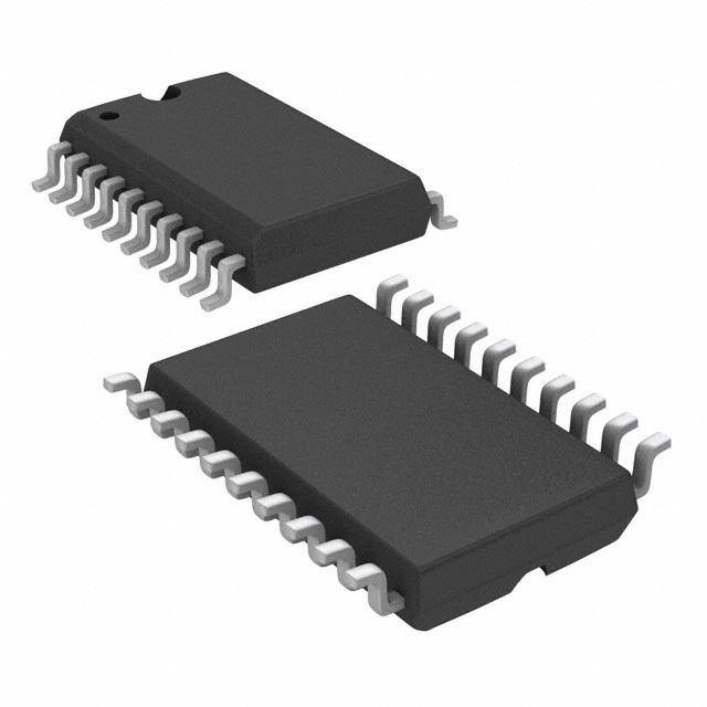
| 封装/外壳 | 20-SOIC(0.295",7.50mm 宽) |
| 封装/箱体 | SOIC-20 Wide |
| 工作温度 | -40°C ~ 85°C |
| 工作电源电压 | 40 V |
| 工作电源电流 | 13 mA |
| 工厂包装数量 | 25 |
| 最大工作温度 | + 85 C |
| 最小工作温度 | - 40 C |
| 标准包装 | 25 |
| 温度监测 | Temperature Monitoring |
| 电压-电源 | 8.8 V ~ 35 V |
| 电池化学 | 铅酸 |
| 电池类型 | Lead Acid |
| 系列 | UC2909 |
| 输出电流 | 2 A |


- 商务部:美国ITC正式对集成电路等产品启动337调查
- 曝三星4nm工艺存在良率问题 高通将骁龙8 Gen1或转产台积电
- 太阳诱电将投资9.5亿元在常州建新厂生产MLCC 预计2023年完工
- 英特尔发布欧洲新工厂建设计划 深化IDM 2.0 战略
- 台积电先进制程称霸业界 有大客户加持明年业绩稳了
- 达到5530亿美元!SIA预计今年全球半导体销售额将创下新高
- 英特尔拟将自动驾驶子公司Mobileye上市 估值或超500亿美元
- 三星加码芯片和SET,合并消费电子和移动部门,撤换高东真等 CEO
- 三星电子宣布重大人事变动 还合并消费电子和移动部门
- 海关总署:前11个月进口集成电路产品价值2.52万亿元 增长14.8%


PDF Datasheet 数据手册内容提取
UC2909 UC3909 Switchmode Lead-Acid Battery Charger FEATURES DESCRIPTION • Accurate and Efficient Control of The UC3909 family of Switchmode Lead-Acid Battery Chargers accurately Battery Charging controls lead acid battery charging with a highly efficient average current modecontrolloop.Thischipcombineschargestatelogicwithaveragecur- • Average Current Mode Control from rentPWMcontrolcircuitry.Chargestatelogiccommandscurrentorvoltage Trickle to Overcharge control depending on the charge state. The chip includes undervoltage • Resistor Programmable Charge lockout circuitry to insure sufficient supply voltage is present before output Currents switchingstarts.Additionalcircuitblocksincludeadifferentialcurrentsense • Thermistor Interface Tracks Battery amplifier, a 1.5% voltage reference, a –3.9mV/°C thermistor linearization Requirements Over Temperature circuit, voltage and current error amplifiers, a PWM oscillator, a PWM com- parator, a PWM latch, charge state decode bits, and a 100mAopen collec- • Output Status Bits Report on Four tor output driver. Internal Charge States • Undervoltage Lockout Monitors VCC and VREF BLOCK DIAGRAM UDG-95007-1 Pin numbers refer to J, N, DW packages. 1/99
UC2909 UC3909 ABSOLUTE MAXIMUM RATINGS Supply Voltage (VCC), OUT, STAT0, STAT1. . . . . . . . . . .40V Output Current Sink . . . . . . . . . . . . . . . . . . . . . . . . . . . . . .0.1A CS+, CS-. . . . . . . . . . . . . . . . . . . . . . . . . .-0.4 to VCC (Note 1) Remaining Pin Voltages. . . . . . . . . . . . . . . . . . . . . .-0.3V to 9V Storage Temperature . . . . . . . . . . . . . . . . . . .-65°C to +150°C Junction Temperature. . . . . . . . . . . . . . . . . . .-55°C to +150°C Lead Temperature (Soldering, 10 sec.). . . . . . . . . . . . .+300°C Allcurrentsarepositiveinto,negativeoutofthespecifiedter- minal.ConsultPackagingSectionofDatabookforthermallimi- tations and considerations of packages. Note1:Voltagesmorenegativethan-0.4Vcanbetoleratedif current is limited to 50mA. CONNECTION DIAGRAMS DIL-20, (Top View) LCC-28, PLCC-28 (Top View) J or N, DW Packages L, Q Packages ELECTRICAL CHARACTERISTICS:Unless otherwise stated these specifications apply for T = –40°C to +85°C for A UC2909; °0C to +70°C for UC3909; C = 330pF, R = 11.5k, R10 = 10k, R = 10k, V = 15V, Output no load, R = T SET THM CC STAT0 R = 10k, CHGENB = OVCTAP = VLOGIC, T = T . STAT1 A J PARAMETER TEST CONDITIONS MIN TYP MAX UNITS Current Sense AMP (CSA) Section V = CS+ – CS– ID DC Gain CS– = 0, CS+ = -50mV; CS+ = –250mV 4.90 5 5.10 V/V CS+ = 0, CS– = 50mV; CS–- = 250mV 4.90 5 5.10 V/V VOFFSET(VCSO– VCAO) CS+ = CS– = 2.3V, CAO = CA– 15 mV CMRR V = –0.25 to VCC – 2, 8.8 < VCC < 14 50 dB CM V = –0.25 to VCC, 14 < VCC < 35 50 dB CM VOL VID= –550mV, –0.25V < VCM < VCC–2, 0.3 0.6 V I = 500m A O VOH VID= +700mV, –0.25V < VCM < VCC–2, 5.2 5.7 6.2 V I = –250m A O Output Source Current V = +700mV, CSO = 4V –1 –0.5 mA ID Output Sink Current V = –550mV, CSO = 1V 3 4.5 mA ID 3dB Bandwidth V = 90mV, V = 0V 200 kHz ID CM 2
UC2909 UC3909 ELECTRICAL CHARACTERISTICS:Unless otherwise stated these specifications apply for T = –40°C to +85°C for A UC2909; °0C to +70°C for UC3909; C = 330pF, R = 11.5k, R10 = 10k, R = 10k, V = 15V, Output no load, R = T SET THM CC STAT0 R = 10k, CHGENB = OVCTAP = VLOGIC, T = T . STAT1 A J PARAMETER TEST CONDITIONS MIN TYP MAX UNITS Current Error Amplifier (CEA) Section IB 8.8V < VCC < 35V, VCHGENB= VLOGIC 0.1 0.8 m A VIO(Note 2) 8.8V < VCC < 35V, CAO = CA– 10 mV AVO 1V < VAO < 4V 60 90 dB GBW T = 25°C, F = 100kHz 1 1.5 MHz J VOL IO= 250m A 0.4 0.6 V VOH IO= –5mA 4.5 5 V Output Source Current CAO = 4V –25 –12 mA Output Sink Current CAO = 1V 2 3 mA ICA–, ITRCK_CONTROL VCHGENB= GND 8.5 10 11.5 m A Voltage Amplifier (CEA) Section IB Total Bias Current; Regulating Level 0.1 1 m A VIO(Note 2) 8.8V < VCC < 35V, VCM = 2.3V, VAO = VA– 1.2 mV AVO 1V < CAO < 4V 60 90 dB GBW T = 25°C, F = 100kHz 0.25 0.5 MHz J VOL IO= 500m A 0.4 0.6 V VOH IO= –500m A 4.75 5 5.25 V Output Source Current CAO = 4V –2 –1 mA Output Sink Current CAO = 1V 2 2.5 mA VAO Leakage: High Impedance State V = GND, STAT0 = 0 & STAT1 = 0, –1 1 m A CHGENB VAO = 2.3V Pulse Width Modulator Section Maximum Duty Cycle CAO = 0.6V 90 95 100 % Modulator Gain CAO = 2.5V, 3.2V 63 71 80 %/V OSC Peak 3 V OSC Valley 1 V Oscillator Section Frequency 8.8V < VCC < 35V 198 220 242 kHz Thermistor Derived Reference Section V = V – V ID RTHM R10 Initial Accuracy, VAO (RTHM = 10k) V = 0, R10 = RTHM =10k (Note 3) 2.2655 2.3 2.3345 V ID V = 0, R10 = RTHM =10k, –40°C£ T < 0°C 2.254 2.3 2.346 V ID A (Note 3) Line Regulation V = 8.8V to 35V 3 10 mV CC VAO RTHM = 138k, R10 = 10k 2.458 2.495 2.532 V RTHM = 138k, R10 = 10k, -40°C£ T < 0°C 2.445 2.495 2.545 V A RTHM = 33.63k, R10 = 10k 2.362 2.398 2.434 V RTHM = 33.63k, R10 = 10k, -40°C£ T < 0°C 2.350 2.398 2.446 V A RTHM = 1.014k, R10 = 10k 2.035 2.066 2.097 V RTHM = 1.014k, R10 = 10k, -40°C£ T < 0°C 2.025 2.066 2.107 V A Charge Enable Comparator Section (CEC) Threshold Voltage As a function of VA– 0.99 1 1.01 V/V Input Bias Current CHGENB = 2.3V –0.5 –0.1 m A 3
UC2909 UC3909 ELECTRICAL CHARACTERISTICS:Unless otherwise stated these specifications apply for T = –40°C to +85°C for A UC2909; °0C to +70°C for UC3909; C = 330pF, R = 11.5k, R10 = 10k, R = 10k, V = 15V, Output no load, R = T SET THM CC STAT0 R = 10k, CHGENB = OVCTAP = VLOGIC, T = T . STAT1 A J PARAMETER TEST CONDITIONS MIN TYP MAX UNITS Voltage Sense Comparator Section (VSC) Threshold Voltage STAT0 = 0, STAT1 = 0, Function of V 0.945 0.95 0.955 V/V REF STAT0 = 1, STAT1 = 0, Function of V 0.895 0.9 0.905 V/V REF Over Charge Taper Current Comparator Section (OCTIC) Threshold Voltage Function of 2.3V REF, CA- = CAO 0.99 1 1.01 V/V Input Bias Current OVCTAP = 2.3V –0.5 –0.1 m A Logic 5V Reference Section (VLOGIC) VLOGIC VCC = 15V 4.875 5.0 5.125 V Line Regulation 8.8V < V < 35V 3 15 mV CC Load Regulation 0 < I < 10mA 3 15 mV O Reference Comparator Turn-on Threshold 4.3 4.8 V Short Circuit Current V = 0V 30 50 80 mA REF Output Stage Section ISINKContinuous 50 mA IPEAK 100 mA VOL IO=50mA 1 1.3 V LeakageCurrent V =35V 25 m A OUT STAT0 & STAT1 Open Collector Outputs Section Maximum Sink Current V = 8.8V 6 10 mA OUT Saturation Voltage I = 5mA 0.1 0.45 V OUT Leakage Current V = 35V 25 m A OUT STATLV Open Collector Outputs Section Maximum Sink Current V = 5V 2.5 5 mA OUT Saturation Voltage I = 2mA 0.1 0.45 V OUT Leakage current V = 5V 3 m A OUT UVLO Section Turn-on Threshold 6.8 7.8 8.8 V Hysteresis 100 300 500 mV ICCSection ICC(run) (See Fig. 1) 13 19 mA ICC(off) VCC = 6.5V 2 mA Note 2: VIO is measured prior to packaging with internal probe pad. Note 3: Thermistor initial accuracy is measured and trimmed with respect to VAO; VAO = VA–. PIN DESCRIPTIONS CA–: The inverting input to the current error amplifier. CSO: The output of the current sense amplifier which is internally clamped to approximately 5.7V. CAO: The output of the current error amplifier which is internally clamped to approximately 4V. It is internally CHGENB: The input to a comparator that detects when connected to the inverting input of the PWM comparator. battery voltage is low and places the charger in a trickle charge state. The charge enable comparator makes the CS–, CS+: The inverting and non-inverting inputs to the output of the voltage error amplifier a high impedance current sense amplifier. This amplifier has a fixed gain of while forcing a fixed 10m A into CA– to set the trickle five and a common-mode voltage range of from –250mV charge current. to +VCC. 4
UC2909 UC3909 PIN DESCRIPTIONS (cont.) GND: The reference point for the internal reference, all thresholds, and the return for the remainder of the de- vice. The output sink transistor is wired directly to this pin. OVCTAP: The overcharge current taper pin detects when the output current has tapered to the float thresh- old in the overcharge state. OSC: Theoscillatorramppinwhichhasacapacitor(C ) T to ground. The ramp oscillates between approximately 1.0V to 3.0V and the frequency is approximated by: 1 frequency= 1.2•C •R T SET OUT: TheoutputofthePWMdriverwhichconsistsofan Figure 1. ICCvs. temperature. open collector output transistor with 100mAsink capabil- ity. STAT1: This open collector pin is the second decode bit R10: Input used to establish a differential voltage corre- used to decode the charge states. sponding to the temperature of the thermistor. Connect STATLV: This bit is high when the charger is in the float a 10k resistor to ground from this point. state. RSET: A resistor to ground programs the oscillator VA–: The inverting input to the voltage error amplifier. charge current and the trickle control current for the oscil- VAO: The output of the voltage error amplifier. The up- lator ramp. per output clamp voltage of this amplifier is 5V. 1.75 The oscillator charge current is approximately . VCC: The input voltage to the chip. The chip is opera- R SET tional between 7.5V and 40V and should be bypassed The trickle control current (ITRCK_CONTROL) is approxi- with a 1m F capacitor. A typical ICC vs. temperature is 0.115 shown in Figure 1. mately . R SET VLOGIC: The precision reference voltage. It should be RTHM: A 10k thermistor is connected to ground and is bypassed with a 0.1m F capacitor. thermally connected to the battery. The resistance will Charge State Decode Chart vary exponentially over temperature and its change is used to vary the internal 2.3V reference by –3.9mV/°C. STAT0 and STAT1 are open collector outputs. The out- The recommended thermistor for this function is part put is approximately 0.2V for a logic 0. number L1005-5744-103-D1, Keystone Carbon Com- pany, St. Marys, PA. STAT1 STAT0 Trickle Charge 0 0 STAT0: This open collector pin is the first decode bit Bulk Charge 0 1 used to decode the charge states. Over Charge 1 0 Float Charge 1 1 5
UC2909 UC3909 APPLICATION INFORMATION A Block Diagram of the UC3909 is shown on the first The VEA, V = 5V clamp saturates the voltage loop OH page, while a Typical Application Circuit is shown in Fig- and consequently limits the charge current as stated in ure2. ThecircuitinFigure2requiresaDCinputvoltage Equation 1. between 12V and 40V. During the trickle bias state the maximum allowable The UC3909 uses a voltage control loop with average charge current (ITC) is similarly determined: cleuardre-anctidlimbitainttgertyo. pTrehceissemlyacllonintcrorelathsee cinhacrogmepraletxeityofoaf ITC=ITRICK_CONTROL•RG1 (2) RS•5 average current limiting is offset by the relative simplicity of the control loop design. ITRCK_CONTROL is the fixed control current into CA–. I is 10m A when R = 11.5k. See RSET CONTROLLOOP TRCK_CONTROL SET pin description for equation. Current Sense Amplifier Current Error Amplifier This amplifier measures the voltage across the sense re- The current error amplifier (CA) compares the output of sistorRSwithafixedgainoffiveandanoffsetvoltageof the current sense amplifier to the output of the voltage 2.3V. This voltage is proportional to the battery current. error amplifier. The output of the CAforces a PWM duty The most positive voltage end of RS is connected to CS- cyclewhichresultsinthecorrectaveragebatterycurrent. ensuring the correct polarity going into the PWM com- With integral compensation, the CAwill have a very high parator. DC current gain, resulting in effectively no average DC CSO = 2.3V when there is zero battery current. current error. For stability purposes, the high frequency gain of the CA must be designed such that the magni- RS is chosen by dividing 350mV by the maximum allow- tude of the down slope of the CA output signal is less able load current. Asmaller value for RS can be chosen than or equal to the magnitude of the up slope of the to reduce power dissipation. PWM ramp. Maximum Charge Current, Ibulk, is set by knowing the CHARGE ALGORITHM maximum voltage error amplifier output, V = 5V, the OH maximum allowable drop across RS, and setting the re- Refer to Figure 3 in UC3906 Data Sheet in the data sistors RG1 and RG2 such that; book. RG1= 5•VRS = 5•VRS = (1) A) Trickle Charge State RG2 VLOGIC–CA– 5V–2.3V STAT0 = STAT1 = STATLV = logic 0 5•V RS =1.852•I •RS When CHGNB is less than VREF (2.3V – 3.9mV/°C), 2.7V BULK STATLV is forced low. This decreases the sense voltage divider ratio, forcing the battery to overcharge (VOC). The maximum allowable drop across RS is specified to limit the maximum swing at CSO to approximately 2.0V (RS1+RS2+RS3 ||RS4) (3) VOC=(VREF)• ( ) to keep the CSO amplifier output from saturating. RS3 ||RS4 No charge/load current: V = 2.3V, CSO During the trickle charge state, the output of the voltage Max charge/load current: V = 2.3V–2.0V = 0.3V error amplifier is high impedance. The trickle control cur- max(CSO) rent is directed into the CA– pin setting the maximum Voltage Error Amplifier: trickle charge current. The trickle charge current is de- The voltage error amplifier (VEA) senses the battery fined in Equation 2. voltage and compares it to the 2.3V – 3.9mV/°C thermis- B) Bulk Charge State tor generated reference. Its output becomes the current STAT1 = STATLV = logic 0, STAT0 = logic 1 command signal and is summed with the current sense As the battery charges, the UC3909 will transition from amplifier output. A 5.0V voltage error amplifier upper trickle to bulk charge when CHGENB becomes greater clamp limits maximum load current. During the trickle than 2.3V. The transition equation is chargestate,thevoltageamplifieroutputisopened(high impedance output) by the charge enable comparator. A VT=VREF•(RS1+RS2+RS3||RS4) (4) trickle bias current is summed into the CA– input which (RS2+RS3||RS4) sets the maximum trickle charge current. STATLV is still driven low. 6
UC2909 UC3909 APPLICATION INFORMATION (cont.) s. e g a k c a p W D N, J, o t er ef r s er b m u n n Pi UDG-95008-1 Figure 2. Typical application circuit 7
UC2909 UC3909 APPLICATION INFORMATION (cont.) During the bulk charge state, the voltage error amplifier D) Float State is now operational and is commanding maximum charge STAT0 = STAT1 = STATLV = logic 1 current (I ) set by Equation 1. The voltage loop at- BULK The battery charge current tapers below its OVCTAP tempts to force the battery to VOC. threshold, and forces STATLV high increasing the volt- C) Overcharge State age sense divider ratio. The voltage loop now forces the STAT0 = STATLV = logic 0, STAT1 = logic 1 battery charger to regulate at its float state voltage (V ). F The battery voltage surpasses 95% of VOC indicating ( )(RS1+RS2+RS3) (6) V = V the UC3909 is in its overcharge state. F REF RS3 During the overcharge charge state, the voltage loop be- If the load drains the battery to less than 90% of V , the F comes stable and the charge current begins to taper off. charger goes back to the bulk charge state, STATE 1. As the charge current tapers off, the voltage at CSO in- OFF LINE APPLICATIONS creases toward its null point of 2.3V. The center connec- tion of the two resistors between CSO and VLOGIC sets For off line charge applications, either Figure 3 or Figure the overcurrent taper threshold (OVCTAP). Knowing the 4 can be used as a baseline. Figure 3 has the advan- desiredoverchargeterminatecurrent(I ),theresistors tage of high frequency operation resulting in a small iso- OCT R andR canbecalculatedbychoosingavalue lation transformer. Figure 4 is a simpler design, but at OVC1 OVC2 of R and using the following equation: the expense of larger magnetics. OVC2 R =(1.8518)•I •RS•R (5) OVC1 OCT OVC2 UDG-95009 Figure 3. Off line charger with primary side PWM 8
UC2909 UC3909 APPLICATION INFORMATION (cont.) UDG-95010 Figure 4. Isolated off line charger UNITRODE CORPORATION 7 CONTINENTALBLVD. • MERRIMACK, NH 03054 TEL. (603) 424-2410 • FAX (603) 424-3460 9
PACKAGE OPTION ADDENDUM www.ti.com 24-Dec-2014 PACKAGING INFORMATION Orderable Device Status Package Type Package Pins Package Eco Plan Lead/Ball Finish MSL Peak Temp Op Temp (°C) Device Marking Samples (1) Drawing Qty (2) (6) (3) (4/5) UC2909DW LIFEBUY SOIC DW 20 25 Green (RoHS CU NIPDAU Level-2-260C-1 YEAR -40 to 85 UC2909DW & no Sb/Br) UC2909DWG4 LIFEBUY SOIC DW 20 25 Green (RoHS CU NIPDAU Level-2-260C-1 YEAR -40 to 85 UC2909DW & no Sb/Br) UC2909DWTR OBSOLETE SOIC DW 20 TBD Call TI Call TI -40 to 85 UC2909DW UC2909DWTRG4 OBSOLETE SOIC DW 20 TBD Call TI Call TI -40 to 85 UC2909N NRND PDIP N 20 20 Green (RoHS SN N / A for Pkg Type -40 to 85 UC2909N & no Sb/Br) UC3909DW LIFEBUY SOIC DW 20 25 Green (RoHS CU NIPDAU Level-2-260C-1 YEAR -20 to 70 UC3909DW & no Sb/Br) UC3909DWG4 LIFEBUY SOIC DW 20 25 Green (RoHS CU NIPDAU Level-2-260C-1 YEAR -20 to 70 UC3909DW & no Sb/Br) UC3909DWTR LIFEBUY SOIC DW 20 2000 Green (RoHS CU NIPDAU Level-2-260C-1 YEAR -20 to 70 UC3909DW & no Sb/Br) UC3909N LIFEBUY PDIP N 20 20 Green (RoHS SN N / A for Pkg Type -20 to 70 UC3909N & no Sb/Br) UC3909NG4 LIFEBUY PDIP N 20 20 Green (RoHS SN N / A for Pkg Type -20 to 70 UC3909N & no Sb/Br) (1) The marketing status values are defined as follows: ACTIVE: Product device recommended for new designs. LIFEBUY: TI has announced that the device will be discontinued, and a lifetime-buy period is in effect. NRND: Not recommended for new designs. Device is in production to support existing customers, but TI does not recommend using this part in a new design. PREVIEW: Device has been announced but is not in production. Samples may or may not be available. OBSOLETE: TI has discontinued the production of the device. (2) Eco Plan - The planned eco-friendly classification: Pb-Free (RoHS), Pb-Free (RoHS Exempt), or Green (RoHS & no Sb/Br) - please check http://www.ti.com/productcontent for the latest availability information and additional product content details. TBD: The Pb-Free/Green conversion plan has not been defined. Pb-Free (RoHS): TI's terms "Lead-Free" or "Pb-Free" mean semiconductor products that are compatible with the current RoHS requirements for all 6 substances, including the requirement that lead not exceed 0.1% by weight in homogeneous materials. Where designed to be soldered at high temperatures, TI Pb-Free products are suitable for use in specified lead-free processes. Pb-Free (RoHS Exempt): This component has a RoHS exemption for either 1) lead-based flip-chip solder bumps used between the die and package, or 2) lead-based die adhesive used between the die and leadframe. The component is otherwise considered Pb-Free (RoHS compatible) as defined above. Green (RoHS & no Sb/Br): TI defines "Green" to mean Pb-Free (RoHS compatible), and free of Bromine (Br) and Antimony (Sb) based flame retardants (Br or Sb do not exceed 0.1% by weight in homogeneous material) Addendum-Page 1
PACKAGE OPTION ADDENDUM www.ti.com 24-Dec-2014 (3) MSL, Peak Temp. - The Moisture Sensitivity Level rating according to the JEDEC industry standard classifications, and peak solder temperature. (4) There may be additional marking, which relates to the logo, the lot trace code information, or the environmental category on the device. (5) Multiple Device Markings will be inside parentheses. Only one Device Marking contained in parentheses and separated by a "~" will appear on a device. If a line is indented then it is a continuation of the previous line and the two combined represent the entire Device Marking for that device. (6) Lead/Ball Finish - Orderable Devices may have multiple material finish options. Finish options are separated by a vertical ruled line. Lead/Ball Finish values may wrap to two lines if the finish value exceeds the maximum column width. Important Information and Disclaimer:The information provided on this page represents TI's knowledge and belief as of the date that it is provided. TI bases its knowledge and belief on information provided by third parties, and makes no representation or warranty as to the accuracy of such information. Efforts are underway to better integrate information from third parties. TI has taken and continues to take reasonable steps to provide representative and accurate information but may not have conducted destructive testing or chemical analysis on incoming materials and chemicals. TI and TI suppliers consider certain information to be proprietary, and thus CAS numbers and other limited information may not be available for release. In no event shall TI's liability arising out of such information exceed the total purchase price of the TI part(s) at issue in this document sold by TI to Customer on an annual basis. OTHER QUALIFIED VERSIONS OF UC2909 : •Enhanced Product: UC2909-EP NOTE: Qualified Version Definitions: •Enhanced Product - Supports Defense, Aerospace and Medical Applications Addendum-Page 2
PACKAGE MATERIALS INFORMATION www.ti.com 17-Aug-2012 TAPE AND REEL INFORMATION *Alldimensionsarenominal Device Package Package Pins SPQ Reel Reel A0 B0 K0 P1 W Pin1 Type Drawing Diameter Width (mm) (mm) (mm) (mm) (mm) Quadrant (mm) W1(mm) UC3909DWTR SOIC DW 20 2000 330.0 24.4 10.8 13.0 2.7 12.0 24.0 Q1 PackMaterials-Page1
PACKAGE MATERIALS INFORMATION www.ti.com 17-Aug-2012 *Alldimensionsarenominal Device PackageType PackageDrawing Pins SPQ Length(mm) Width(mm) Height(mm) UC3909DWTR SOIC DW 20 2000 367.0 367.0 45.0 PackMaterials-Page2
IMPORTANTNOTICE TexasInstrumentsIncorporatedanditssubsidiaries(TI)reservetherighttomakecorrections,enhancements,improvementsandother changestoitssemiconductorproductsandservicesperJESD46,latestissue,andtodiscontinueanyproductorserviceperJESD48,latest issue.Buyersshouldobtainthelatestrelevantinformationbeforeplacingordersandshouldverifythatsuchinformationiscurrentand complete.Allsemiconductorproducts(alsoreferredtohereinas“components”)aresoldsubjecttoTI’stermsandconditionsofsale suppliedatthetimeoforderacknowledgment. TIwarrantsperformanceofitscomponentstothespecificationsapplicableatthetimeofsale,inaccordancewiththewarrantyinTI’sterms andconditionsofsaleofsemiconductorproducts.TestingandotherqualitycontroltechniquesareusedtotheextentTIdeemsnecessary tosupportthiswarranty.Exceptwheremandatedbyapplicablelaw,testingofallparametersofeachcomponentisnotnecessarily performed. TIassumesnoliabilityforapplicationsassistanceorthedesignofBuyers’products.Buyersareresponsiblefortheirproductsand applicationsusingTIcomponents.TominimizetherisksassociatedwithBuyers’productsandapplications,Buyersshouldprovide adequatedesignandoperatingsafeguards. TIdoesnotwarrantorrepresentthatanylicense,eitherexpressorimplied,isgrantedunderanypatentright,copyright,maskworkright,or otherintellectualpropertyrightrelatingtoanycombination,machine,orprocessinwhichTIcomponentsorservicesareused.Information publishedbyTIregardingthird-partyproductsorservicesdoesnotconstitutealicensetousesuchproductsorservicesorawarrantyor endorsementthereof.Useofsuchinformationmayrequirealicensefromathirdpartyunderthepatentsorotherintellectualpropertyofthe thirdparty,oralicensefromTIunderthepatentsorotherintellectualpropertyofTI. ReproductionofsignificantportionsofTIinformationinTIdatabooksordatasheetsispermissibleonlyifreproductioniswithoutalteration andisaccompaniedbyallassociatedwarranties,conditions,limitations,andnotices.TIisnotresponsibleorliableforsuchaltered documentation.Informationofthirdpartiesmaybesubjecttoadditionalrestrictions. ResaleofTIcomponentsorserviceswithstatementsdifferentfromorbeyondtheparametersstatedbyTIforthatcomponentorservice voidsallexpressandanyimpliedwarrantiesfortheassociatedTIcomponentorserviceandisanunfairanddeceptivebusinesspractice. TIisnotresponsibleorliableforanysuchstatements. Buyeracknowledgesandagreesthatitissolelyresponsibleforcompliancewithalllegal,regulatoryandsafety-relatedrequirements concerningitsproducts,andanyuseofTIcomponentsinitsapplications,notwithstandinganyapplications-relatedinformationorsupport thatmaybeprovidedbyTI.Buyerrepresentsandagreesthatithasallthenecessaryexpertisetocreateandimplementsafeguardswhich anticipatedangerousconsequencesoffailures,monitorfailuresandtheirconsequences,lessenthelikelihoodoffailuresthatmightcause harmandtakeappropriateremedialactions.BuyerwillfullyindemnifyTIanditsrepresentativesagainstanydamagesarisingoutoftheuse ofanyTIcomponentsinsafety-criticalapplications. Insomecases,TIcomponentsmaybepromotedspecificallytofacilitatesafety-relatedapplications.Withsuchcomponents,TI’sgoalisto helpenablecustomerstodesignandcreatetheirownend-productsolutionsthatmeetapplicablefunctionalsafetystandardsand requirements.Nonetheless,suchcomponentsaresubjecttotheseterms. NoTIcomponentsareauthorizedforuseinFDAClassIII(orsimilarlife-criticalmedicalequipment)unlessauthorizedofficersoftheparties haveexecutedaspecialagreementspecificallygoverningsuchuse. OnlythoseTIcomponentswhichTIhasspecificallydesignatedasmilitarygradeor“enhancedplastic”aredesignedandintendedforusein military/aerospaceapplicationsorenvironments.BuyeracknowledgesandagreesthatanymilitaryoraerospaceuseofTIcomponents whichhavenotbeensodesignatedissolelyattheBuyer'srisk,andthatBuyerissolelyresponsibleforcompliancewithalllegaland regulatoryrequirementsinconnectionwithsuchuse. TIhasspecificallydesignatedcertaincomponentsasmeetingISO/TS16949requirements,mainlyforautomotiveuse.Inanycaseofuseof non-designatedproducts,TIwillnotberesponsibleforanyfailuretomeetISO/TS16949. Products Applications Audio www.ti.com/audio AutomotiveandTransportation www.ti.com/automotive Amplifiers amplifier.ti.com CommunicationsandTelecom www.ti.com/communications DataConverters dataconverter.ti.com ComputersandPeripherals www.ti.com/computers DLP®Products www.dlp.com ConsumerElectronics www.ti.com/consumer-apps DSP dsp.ti.com EnergyandLighting www.ti.com/energy ClocksandTimers www.ti.com/clocks Industrial www.ti.com/industrial Interface interface.ti.com Medical www.ti.com/medical Logic logic.ti.com Security www.ti.com/security PowerMgmt power.ti.com Space,AvionicsandDefense www.ti.com/space-avionics-defense Microcontrollers microcontroller.ti.com VideoandImaging www.ti.com/video RFID www.ti-rfid.com OMAPApplicationsProcessors www.ti.com/omap TIE2ECommunity e2e.ti.com WirelessConnectivity www.ti.com/wirelessconnectivity MailingAddress:TexasInstruments,PostOfficeBox655303,Dallas,Texas75265 Copyright©2014,TexasInstrumentsIncorporated