
 Datasheet下载
- 型号: MAX14572EUD+
- 制造商: Maxim
- 库位|库存: xxxx|xxxx
- 要求:
| 数量阶梯 | 香港交货 | 国内含税 |
| +xxxx | $xxxx | ¥xxxx |
查看当月历史价格
查看今年历史价格
MAX14572EUD+产品简介:
ICGOO电子元器件商城为您提供MAX14572EUD+由Maxim设计生产,在icgoo商城现货销售,并且可以通过原厂、代理商等渠道进行代购。 MAX14572EUD+价格参考¥31.23-¥31.23。MaximMAX14572EUD+封装/规格:电涌抑制 IC, 。您可以下载MAX14572EUD+参考资料、Datasheet数据手册功能说明书,资料中有MAX14572EUD+ 详细功能的应用电路图电压和使用方法及教程。
Maxim Integrated(现为Analog Devices旗下品牌)的MAX14572EUD+是一款电涌抑制IC,主要用于保护电子设备免受电压浪涌和静电放电(ESD)等瞬态干扰的损害。其应用场景主要包括以下几个方面:

1. 工业自动化设备:在工业控制系统中,用于保护PLC、传感器、通信接口等关键电路,防止因电源或信号线上的电压突变而导致设备损坏。

2. 通信设备:适用于路由器、交换机、基站等通信设备的电源和数据接口保护,确保设备在恶劣电磁环境中稳定运行。

3. 消费电子产品:如笔记本电脑、平板电脑和智能手机的充电接口、USB接口等,提供对静电放电和电源浪涌的防护,提升产品可靠性。

4. 汽车电子系统:用于车载信息娱乐系统、ECU模块、车载充电器等,保护电子部件免受车辆电源系统中常见的电压尖峰影响。

5. 医疗设备:保护精密医疗仪器的输入输出接口,确保设备在频繁插拔或雷击感应等情况下仍能安全运行。

MAX14572EUD+具有低电容、快速响应时间和高可靠性等特点,适用于需要高性能保护的高速信号线和电源线路。
| 参数 | 数值 |
| 产品目录 | |
| 描述 | IC ADJ OV/OC PROTECTOR 14TSSOP监控电路 Adj Over-V/C Protector |
| 产品分类 | |
| 品牌 | Maxim Integrated |
| 产品手册 | |
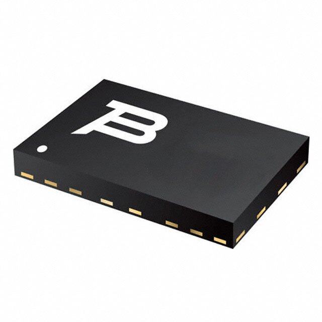
| 产品图片 |
|
| rohs | 符合RoHS无铅 / 符合限制有害物质指令(RoHS)规范要求 |
| 产品系列 | 电源管理 IC,监控电路,Maxim Integrated MAX14572EUD+- |
| NumberofInputsMonitored | 1 Input |
| 数据手册 | |
| 产品型号 | MAX14572EUD+ |
| 产品种类 | 监控电路 |
| 人工复位 | No Manual Reset |
| 供应商器件封装 | 14-TSSOP-EP |
| 功率(W) | - |
| 包装 | 管件 |
| 商标 | Maxim Integrated |
| 安装风格 | SMD/SMT |
| 封装 | Tube |
| 封装/外壳 | 14-TSSOP (0.173",4.40mm 宽)裸焊盘 |
| 封装/箱体 | TSSOP-14 |
| 工作电源电流 | 490 uA |
| 工厂包装数量 | 96 |
| 应用 | 通用 |
| 技术 | 混合技术 |
| 最大功率耗散 | 2051.3 mW |
| 最大工作温度 | + 85 C |
| 最小工作温度 | - 40 C |
| 标准包装 | 1 |
| 欠电压阈值 | 19.2 V |
| 电压-工作 | 36V |
| 电压-箝位 | - |
| 电池备用开关 | No Backup |
| 电源电压-最大 | 36 V |
| 电源电压-最小 | 4.5 V |
| 电路数 | 1 |
| 监视器 | No Watchdog |
| 类型 | Voltage Supervisory |
| 系列 | MAX14572 |
| 被监测输入数 | 1 Input |
| 输出类型 | Active Low, Open Drain |
| 过电压阈值 | 33 V |
| 阈值电压 | Adjustable |
| 零件号别名 | MAX14572 |


- 商务部:美国ITC正式对集成电路等产品启动337调查
- 曝三星4nm工艺存在良率问题 高通将骁龙8 Gen1或转产台积电
- 太阳诱电将投资9.5亿元在常州建新厂生产MLCC 预计2023年完工
- 英特尔发布欧洲新工厂建设计划 深化IDM 2.0 战略
- 台积电先进制程称霸业界 有大客户加持明年业绩稳了
- 达到5530亿美元!SIA预计今年全球半导体销售额将创下新高
- 英特尔拟将自动驾驶子公司Mobileye上市 估值或超500亿美元
- 三星加码芯片和SET,合并消费电子和移动部门,撤换高东真等 CEO
- 三星电子宣布重大人事变动 还合并消费电子和移动部门
- 海关总署:前11个月进口集成电路产品价值2.52万亿元 增长14.8%


PDF Datasheet 数据手册内容提取
EVALUATION KIT AVAILABLE MAX14571/MAX14572/ Adjustable Overvoltage and Overcurrent MAX14573 Protectors with High Accuracy General Description Benefits and Features The MAX14571/MAX14572/MAX14573 adjustable over- ● Integrated Protection Increases System Reliability voltage and overcurrent-protection devices are ideal to ● Adjustable OVLO and UVLO Thresholds protect systems against positive and negative input volt- (±3% Accurate Preset Thresholds) age faults up to ±40V and feature low 100mΩ(typ) RON ● Automatic Internal and External Selection FETs. ● Programmable Forward Current Limit (Adjustable Up The overvoltage-protector (OVP) feature protects volt- to 4.2A) with ±15% Accuracy ages between 6V and 36V, while the undervoltage-protector (UVP) feature protects voltages between 4.5V and 24V. ● Thermal-Shutdown Protection The overvoltage-lockout (OVLO) and undervoltage-lockout ● 100mΩ (typ) On-Resistance FET (UVLO) thresholds are set using optional external resistors. ● Special Features Facilitate Designs for Industrial The factory-preset internal OVLO threshold is 33V (typ) and Applications the preset internal UVLO threshold is 19.2V (typ). ● Wide 4.5V to 36V Operating Input Range The ICs also feature programmable current-limit protec- tion up to 4.2A. Once current reaches the threshold, ● Reverse-Current Flow Option for Inductive Loads the MAX14571 turns off after the 20.7ms (typ) blanking ● Independent Microprocessor Enable Input (EN) and time and stays off during the retry period. The MAX14572 High-Voltage-Capable Input (HVEN) latches off after the blanking time, and the MAX14573 limits the current continuously. In addition, these devices feature Applications reverse current and thermal-shutdown protection. ● Industrial Equipment The ICs are available in a small 14-pin TSSOP (5mm ● Consumer Electronics x 6.5mm) package and are specified over the extended ● Marine Equipment -40°C to +85°C temperature range. ● Battery-Powered Applications Ordering Information appears at end of data sheet. Typical Operating Circuit VPOWER IN OUT CIN IN OUT COUT IN OUT R3 R1 MAX14571 VPULLUP SYSTEM SYSTEM MAX14572 INPUT MAX14573 UVLO FLAG OVLO EN SETI RIEN R4 R2 HVEN GND NOTE: R1, R2, R3, AND R4 ARE ONLY REQUIRED FOR ADJUSTABLE OVLO/UVLO; OTHERWISE, CONNECT UVLO/OVLO TO GND. 19-6470; Rev 4; 7/17
MAX14571/MAX14572/ Adjustable Overvoltage and Overcurrent MAX14573 Protectors with High Accuracy Absolute Maximum Ratings (All voltages referenced to GND.) Continuous Power Dissipation (TA = +70NC) IN, HVEN ................................................................-40V to +40V TSSOP (derate 25.6mW/NC above +70NC) .......….2051.3mW IN to OUT ...............................................................-40V to +40V Operating Temperature Range ...........................-40NC to +85NC OUT ......................................................................-0.3V to +40V Junction Temperature .........................................………..+150NC OVLO, UVLO, FLAG, EN, RIEN...........................-0.3V to +6.0V Storage Temperature Range ............................-65NC to +150NC Current into IN (DC Operating) (Note 1) ..............………….4.2A Lead Temperature (soldering, 10s) ...................…………+300NC SETI..........................………….-0.3V to Min (VIN, 1.22V) + 0.3V Soldering Temperature (reflow) .........................…………+260NC Stresses beyond those listed under “Absolute Maximum Ratings” may cause permanent damage to the device. These are stress ratings only, and functional operation of the device at these or any other conditions beyond those indicated in the operational sections of the specifications is not implied. Exposure to absolute maximum rating conditions for extended periods may affect device reliability. Note 1: DC current is also limited by the thermal design of the system. Package Information PACKAGE TYPE: 14 TSSOP Package Code U14E+3 Outline Number 21-0108 Land Pattern Number 90-0119 THERMAL RESISTANCE, FOUR-LAYER BOARD Junction to Ambient (θJA) +39°C/W Junction to Case (θJC) +3°C/W For the latest package outline information and land patterns (footprints), go to www.maximintegrated.com/packages. Note that a “+”, “#”, or “-” in the package code indicates RoHS status only. Package drawings may show a different suffix character, but the drawing pertains to the package regardless of RoHS status. Package thermal resistances were obtained using the method described in JEDEC specification JESD51-7, using a four-layer board. For detailed informa¬tion on package thermal considerations, refer to www.maximintegrated.com/thermal-tutorial. Electrical Characteristics (VIN = 4.5V to 36V, TA = -40NC to +85NC, unless otherwise noted. Typical values are at VIN = 24V, RSETI = 12kI, TA = +25°C.) (Note 2) PARAMETER SYMBOL CONDITIONS MIN TYP MAX UNITS IN Voltage Range VIN 4.5 36 V Shutdown Input Current ISHDN VEN = 0V, VHVEN = 5V 15 FA Shutdown Output Current IOFF VOUT = 0V 2 FA Reverse Input Current IIN_RVS VIN = -40V, VOUT = VGND = 0V -35 FA Supply Current IIN VIN = 15V, RISET = 12kI 490 700 FA VIN rising 32 33 34 Internal Overvoltage Trip Level VOVLO V VIN falling 32 VIN falling 17.5 18.5 19.5 Internal Undervoltage Trip Level VUVLO V VIN rising 18.2 19.2 20.2 Overvoltage-Lockout Hysteresis % of typical OVLO 3 % www.maximintegrated.com Maxim Integrated │ 2
MAX14571/MAX14572/ Adjustable Overvoltage and Overcurrent MAX14573 Protectors with High Accuracy Electrical Characteristics (continued) (VIN = 4.5V to 36V, TA = -40NC to +85NC, unless otherwise noted. Typical values are at VIN = 24V, RSETI = 12kI, TA = +25°C.) (Note 2) PARAMETER SYMBOL CONDITIONS MIN TYP MAX UNITS External OVLO Adjustment Range (Note 3) 6 36 V External OVLO Select Voltage VOVLOSEL 0.3 0.50 V External OVLO Leakage Current IOVLO_LEAK VOVLO < 1.2V (Note 4) -100 +100 nA External UVLO Adjustment Range 4.5 24 V External UVLO Select Voltage VOVLOSEL 0.3 0.50 V External UVLO Leakage Current IUVLO_LEAK (Note 4) -100 +100 nA BG Reference Voltage VBG 1.186 1.210 1.234 V INTERNAL FETs Internal FET On-Resistance RON ILOAD = 100mA, VIN R 8V 100 160 mI Current-Limit Adjustment Range ILIM (Notes 4, 5) 0.7 4.2 A Current-Limit Accuracy -15 +15 % FTLhAreGsh Aosldsertion Drop Voltage VFA Ianscsreeratss,e V (IVNI N= -2 V4OVUT) drop until FLAG 560 mV Reverse Current Blocking Threshold VRIB VOUT - VIN 40 100 160 mV Reverse Blocking Leakage Current IRBL VOUT - VIN > 160mV, current into OUT 400 600 FA FLAG OUTPUT FLAG Output Logic-Low Voltage ISINK = 1mA 0.4 V FLAG Output Leakage Current VIN = VFLAG = 5V, FLAG desasserted 2 FA LOGIC INPUT HVEN Threshold Voltage VHVEN_TH 1 2 3.5 V HVEN Threshold Hysteresis 2 % HVEN Input Leakage Current IHVEN_LEAK VHVEN = 36V 26 40 FA HVEN Input Reverse Leakage Current IHVEN_RLEAK VIN = VHVEN = -36V -45 -27 FA EN, RIEN Input Logic-High VIH 1.4 V EN, RIEN Input Logic-Low VIL 0.4 V EN, RIEN Input Leakage Current IRIEINEN_L_ELAEAKK, VEN = VRIEN = 5.0V -1 +1 FA THERMAL PROTECTION Thermal Shutdown TJC_MAX Low-to-high temperature 150 NC Thermal-Shutdown Hysteresis TJC_HYST High-to-low temperature 30 NC TIMING CHARACTERISTICS (Note 6) Switch Turn-On Time tON F2r4o0mI ,O CFOFU toT =IN 4, 7s0eFeF Table 1. RLOAD = 25 ms Switch Turn-Off Time tOFF RLOAD = 47I 3 Fs www.maximintegrated.com Maxim Integrated │ 3
MAX14571/MAX14572/ Adjustable Overvoltage and Overcurrent MAX14573 Protectors with High Accuracy Electrical Characteristics (continued) (VIN = 4.5V to 36V, TA = -40NC to +85NC, unless otherwise noted. Typical values are at VIN = 24V, RSETI = 12kI, TA = +25°C.) (Note 2) PARAMETER SYMBOL CONDITIONS MIN TYP MAX UNITS Overvoltage Switch Turn-Off Time tOFF_OVP VRILNO >AD V =O V4L7OI t,o R VSOEUTIT = = 1 800k%I of VOVLO, 3 Fs Overcurrent Switch Turn-Off Time tOFF_OCP IIN > ILIM, after tBLANK, ILIM = 1A 3 Fs IN Debounce Time tDEB VVIUNV cLOha tnog VeOs UfrTo =m 100V% to o gf rVeINater than 15.0 16.7 18.4 ms Blanking Time tBLANK 18.6 20.7 22.8 ms Autoretry Time tRETRY AFLftAerG b clalenakrin (gd etiamses efrrtoiomn )I O(NUoT t>e 7IL)IM to 540 600 660 ms ESD PROTECTION Human Body Model, IN bypassed IN to GND with a 1FF low-ESR ceramic Q15 kV capacitor Note 2: All units are 100% production tested at TA = +25NC. Limits over the operating temperature range are guaranteed by design and characterization; not production tested. Note 3: Not production tested, user settable. See overvoltage/undervoltage lockout instructions. Note 4: Guaranteed by design; not production tested. UVLO and OVLO are internally clamped to BG reference voltage. Note 5: The current limit can be set below 700mA with a decreased accuracy. Note 6: All timing is measured using 20% and 80% levels. Note 7: The ratio between the autoretry time and blanking time is fixed and equal to 30. Timing Diagrams AUTORETRY VERSIONS tBLANK tRETRY tBLANK tRETRY tBLANK tBLANK tRETRY OUT THE DEVICE COMES OUT OF THERMAL CURRENT LIMIT SHUTDOWN MODE LOAD CURRENT THE DEVICE GOES TO THERMAL SHUTDOWN MODE FLAG NOTE: TIME NOT IN SCALE Figure 1. Autoretry Fault Diagram www.maximintegrated.com Maxim Integrated │ 4
MAX14571/MAX14572/ Adjustable Overvoltage and Overcurrent MAX14573 Protectors with High Accuracy Timing Diagrams (continued) LATCH VERSION tBLANK tBLANK OUT CURRENT LIMIT LOAD CURRENT THE DEVICE GOES THE DEVICE COMES TO THERMAL OUT OF THERMAL SHUTDOWN MODE SHUTDOWN MODE INPUT OR EN CYCLE FLAG NOTE: TIME NOT IN SCALE Figure 2. Latch-Off Fault Diagram CONTINUOUS VERSIONS tBLANK OUT THE DEVICE COMES OUT OF CURRENT LIMIT THERMAL SHUTDOWN MODE LOAD CURRENT THE DEVICE GOES TO THERMAL SHUTDOWN MODE FLAG NOTE: TIME NOT IN SCALE Figure 3. Continuous Fault Diagram www.maximintegrated.com Maxim Integrated │ 5
MAX14571/MAX14572/ Adjustable Overvoltage and Overcurrent MAX14573 Protectors with High Accuracy Timing Diagrams (continued) < tDEB < tDEB tDEB UVLO THRESHOLD VIN ON SWITCH OFF STATUS NOTE: TIME NOT IN SCALE Figure 4. Debounce Timing Typical Operating Characteristics (TA = +25°C, unless otherwise noted.) IN SUPPLY CURRENT IN SUPPLY CURRENT NORMALIZED ON-RESISTANCE vs. SUPPLY VOLTAGE vs. TEMPERATURE vs. SUPPLY VOLTAGE 1.0 1.0 1.3 00..89 SETI UNCONNECTED MAX14571 toc01 00..89 SETI UNCONNECTED MAX14571 toc02 CE 1.2 MAX14571 toc03 ENT (mA) 00..67 TA = +85°C ENT (mA) 00..67 RESISTAN 1.1 TA = +85°C TA = +25°C URR 0.5 URR 0.5 ON- 1.0 SUPPLY C 00..34 SUPPLY C 00..34 RMALIZED 0.9 TA = -40°C O 0.2 TA = +25°C TA = -40°C 0.2 N 0.8 0.1 0.1 VIN = +24V IOUT = 100mA 0 0 0.7 5 10 15 20 25 30 35 40 -40 -15 10 35 60 85 12 15 18 21 24 SUPPLY VOLTAGE (V) TEMPERATURE (°C) SUPPLY VOLTAGE (V) www.maximintegrated.com Maxim Integrated │ 6
MAX14571/MAX14572/ Adjustable Overvoltage and Overcurrent MAX14573 Protectors with High Accuracy Typical Operating Characteristics (continued) (TA = +25°C, unless otherwise noted.) NORMALIZED ON-RESISTANCE NORMALIZED CURRENT LIMIT NORMALIZED CURENT LIMIT vs. TEMPERATURE vs. SUPPLY VOLTAGE vs. TEMPERATURE N-RESISTANCE 11111.....12345 MAX14571 toc04 URRENT LI MIT 11111.....0000124680 MAX14571 toc05 URRENT LI MIT 11111.....0000124680 MAX14571 toc06 O 1.0 C 1.00 C 1.00 D D D ALIZE 0.9 ALIZE 0.98 ALIZE 0.98 M 0.8 M 0.96 M 0.96 R R R O O O N 0.7 N 0.94 N 0.94 0.6 0.92 0.92 VIN = +24V RSETI = 17.4kI VIN = +24V 0.5 0.90 0.90 -40 -15 10 35 60 85 5 8 11 14 17 20 23 26 29 32 35 -40 -15 10 35 60 85 TEMPERATURE (°C) SUPPLY VOLTAGE (V) TEMPERATURE (°C) NORMALIZED OVLO THRESHOLD NORMALIZED UVLO THRESHOLD SHUTDOWN SUPPLY CURRENT vs. TEMPERATURE vs. TEMPERATURE vs. TEMPERATURE OLD 111...001680 MAX14571 toc07 OLD 111...001680 MAX14571 toc08 T (µA) 2205 MAX14571 toc09 H H N RES 1.04 RES 1.04 RRE H H U T 1.02 T 1.02 C 15 O O Y OVL 1.00 UVL 1.00 PPL LIZED 0.98 LIZED 0.98 WN SU 10 NORMA 00..9946 NORMA 00..9946 HUTDO 5 EVNIN == L+O2W4V S HVEN = 100kI PULLUP TO VIN 0.92 0.92 OUT = OVLO = UVLO = GND VIN = +24V VIN = +24V 0.90 0.90 0 -40 -15 10 35 60 85 -40 -15 10 35 60 85 -40 -15 10 35 60 85 TEMPERATURE (°C) TEMPERATURE (°C) TEMPERATURE (°C) SHUTDOWN REVERSE CURRENT TURN-ON TIME TURN-OFF TIME vs. TEMPERATURE vs. TEMPERATURE vs. TEMPERATURE 35 20 100 T (µA) 30 MAX14571 toc10 1168 MAX14571 toc11 8900 MAX14571 toc12 WN SUPPLY CURREN 122505 URN-ON TIME (ms) 1118024 URN-OFF TIME (µs) 45670000 DO 10 VIN = -24V T 6 T 30 HUT EN = LOW 4 20 EN TRANSITION TO 90% OF VOUT S 5 HOVUETN = =O 1V0L0Ok I= U PVULLOL U= PG TNOD VIN 2 EN TRANSITION TO 10% OF VIN 10 CRLOOUATD = = 1 408µ0FI 0 0 0 -40 -15 10 35 60 85 -40 -15 10 35 60 85 -40 -15 10 35 60 85 TEMPERATURE (°C) TEMPERATURE (°C) TEMPERATURE (°C) www.maximintegrated.com Maxim Integrated │ 7
MAX14571/MAX14572/ Adjustable Overvoltage and Overcurrent MAX14573 Protectors with High Accuracy Pin Configuration TOP VIEW IN 1 + 14 OUT IN 2 13 OUT IN 3 12 OUT MAX14571 UVLO 4 11 FLAG MAX14572 OVLO 5 MAX14573 10 EN SETI 6 9 RIEN GND 7 *EP 8 HVEN TSSOP *CONNECT EXPOSED PAD TO GND Pin Description PIN NAME FUNCTION Overvoltage-Protection Input. Bypass IN to GND with a 1FF ceramic capacitor placed as close 1, 2, 3 IN as possible to the device. Use a 1FF, low-ESR ceramic capacitor to enable Q15kV (HBM) ESD protection on IN. For hot-plug applications, see the Applications Information section. Externally Programmable Undervoltage-Lockout Threshold. Connect UVLO to GND to use the 4 UVLO default internal UVLO threshold. Connect UVLO to an external resistor-divider to define a threshold externally and override the preset internal UVLO threshold. Externally Programmable Overvoltage-Lockout Threshold. Connect OVLO to GND to use the 5 OVLO default internal OVLO threshold. Connect OVLO to an external resistor-divider to define a threshold externally and override the preset internal OVLO threshold. Overload Current-Limit Adjust. Connect a resistor from SETI to GND to program the overcurrent 6 SETI limit. If SETI is unconnected, the current limit is set to 0A. If SETI is connected to GND, the FETs turn off and FLAG is asserted. Do not connect more than 10pF to SETI. 7 GND Ground Active-Low Enable Input. HVEN is a high-voltage-capable enable input. Drive HVEN low for normal 8 HVEN operation. Drive HVEN high to disable the device. HVEN has up to 36V overvoltage protection at the input (Table 1). Reverse-Current Enable Input. Connect RIEN to GND to disable the reverse-current flow protection. 9 RIEN Connect RIEN to logic-high to activate the reverse-current flow protection. Active-High Enable Input. Drive EN high for normal operation. Drive EN low to disable the device 10 EN (Table 1). Open-Drain, Fault Indicator Output. FLAG goes low when the fault duration exceeds the blanking 11 FLAG time, reverse current is detected, thermal-shutdown mode is active, OVLO threshold is reached, or SETI is connected to GND. Output Voltage. Output of internal FETs. Bypass OUT to GND with a 1FF ceramic capacitor placed 12, 13, 14 OUT as close as possible to the device. For a long output cable or inductive lead, see the Applications Information section. Exposed Pad. Internally connected to GND. Connect EP to a large ground plane to maximize — EP thermal performance. Do not use EP as the single GND connection. www.maximintegrated.com Maxim Integrated │ 8
MAX14571/MAX14572/ Adjustable Overvoltage and Overcurrent MAX14573 Protectors with High Accuracy Functional Diagram MAX14571 MAX14572 MAX14573 IN OUT OUT IN OUT REVERSE-INPUT REVERSE-CURRENT RIEN PROTECTION IN FLAG N VBG CONTROL LOGIC EN UVLO VSEL HVEN THERMAL SHUTDOWN OVLO VSEL SETI GND www.maximintegrated.com Maxim Integrated │ 9
MAX14571/MAX14572/ Adjustable Overvoltage and Overcurrent MAX14573 Protectors with High Accuracy Detailed Description is off, there is no current through the switch. Thus, the output current is much less than the programmed current The MAX14571/MAX14572/MAX14573 are adjust- limit. Calculate the average output current using the fol- able overvoltage- and overcurrent-protection devices lowing equation: designed to protect systems against positive and nega- tive input voltage faults up to Q40V, and feature low t 100mΩ (typ) on-resistance FETs. If the input voltage ILOAD =ILIM BLANK tBLANK +tRETRY exceeds the OVLO threshold or falls below the UVLO, the internal FETs are turned off to prevent damage to the With a 20.7ms (typ) tBLANK and 600ms (typ) tRETRY, the protected components. If the OVLO or the UVLO pin is duty cycle is 3.3%, resulting in a 96.7% power savings. set below the external OVLO or UVLO select thresholds (VOVLOSEL and VUVLOSEL), the device automatically Latch-Off (MAX14572) selects the internal Q3% (typ) accurate trip thresholds. When the current threshold is reached, the tBLANK timer The internal OVLO threshold is preset to 33V (typ), and begins counting. The FLAG asserts if the overcurrent the internal UVLO threshold is preset to 19.2V (typ). condition is present for tBLANK. The timer resets when The ICs feature programmable current-limit protection the overcurrent condition disappears before tBLANK has up to 4.2A. Once current reaches the threshold, the elapsed. The switch turns off and stays off if the over- MAX14571 turns off after 20.7ms (typ) blanking time and current condition continues beyond the blanking time. stays off during the retry period. The MAX14572 latches To reset the switch, either toggle the control logic EN or off after the blanking time, and the MAX14573 limits the HVEN or cycle the input voltage. If the die temperature current continuously. exceeds +150NC (typ) due to self-heating, the MAX14572 latches off (Figure 2). Programmable Current Limit/Threshold Continuous Current Limit (MAX14573) A resistor from SETI to GND sets the current limit/ threshold for the switch (see the Setting the Current Limit/ When the current threshold is reached, the MAX14573 Threshold section). If the output current is limited at the limits the output current to the programmed current limit. current threshold value for a time equal to or longer than The FLAG asserts if the overcurrent condition is present tBLANK, the output FLAG asserts and the MAX14571 for tBLANK and deasserts when the overload condition is enters the autoretry mode, the MAX14572 latches off the removed. If the die temperature exceeds +150NC (typ) due switch, and the MAX14573 enters the continuous current- to self-heating, the MAX14573 enables thermal shutdown limit mode. until the die temperature drops by approximately 30NC (Figure 3). Autoretry (MAX14571) Reverse-Current Enable (RIEN) When the current threshold is reached, the tBLANK timer begins counting. The FLAG asserts if the overcurrent This feature disables the reverse-current protection condition is present for tBLANK. The timer resets if the and enables reverse-current flow from OUT to IN. The overcurrent condition disappears before tBLANKK has reverse-current enable feature is useful in applications elapsed. A retry time delay, tRETRY, is started immediately with inductive loads. after tBLANK has elapsed and during tRETRY time, the Fault Flag Output FETs are off. At the end of tRETRY, the FETs are turned FLAG is an open-drain fault indicator output and requires on again. If the fault still exists, the cycle is repeated and the FLAG stays low. When the fault is removed, the FETs an external pullup resistor to a DC supply. FLAG goes low stay on. If the die temperature exceeds +150NC (typ) due when any of the following conditions occur: to self-heating, the MAX14571 enables thermal shutdown • The blanking time has elapsed. until the die temperature drops by approximately 30NC • The reverse-current protection has tripped. (Figure 1). • The die temperature exceeds +150NC. The autoretry feature reduces the system power in case of overcurrent or short-circuit conditions. During tBLANK • SETI is connected to ground. time, when the switch is on, the supply current is held at • OVLO threshold is reached. the current limit. During tRETRY time, when the switch www.maximintegrated.com Maxim Integrated │ 10
MAX14571/MAX14572/ Adjustable Overvoltage and Overcurrent MAX14573 Protectors with High Accuracy Thermal-Shutdown Protection Input Debounce Protection The devices have a thermal-shutdown feature to pro- The ICs feature input debounce protection. When the tect them from overheating. The devices turn off and the input voltage is higher than the UVLO threshold voltage FLAG asserts when the junction temperature exceeds for a period greater than the debounce time (tDEB), the +150NC (typ). The devices exit thermal shutdown and internal FETs are turned on. This feature is intended for resume normal operation after the junction temperature applications where the EN or HVEN signal is present cools by 30NC (typ), except for the MAX14572, which re- when the power supply ramps up (Figure 4). mains latched off. Applications Information The thermal limit behaves similarly to the current limit. For the MAX14571 (autoretry), the thermal limit works with the Setting the Current Limit/Threshold autoretry timer. When the device comes out of the thermal A resistor from SETI to ground programs the current limit/ limit, it starts after the retry time. For the MAX14572 (latch threshold value for the devices. Leaving SETI uncon- off), the device latches off until power or EN cycle. For the nected selects a 0A current limit/threshold. Connecting MAX14573 (continuous), the device only disables while SETI to ground asserts FLAG. Use the following formula the temperature is over the limit. There is no blanking time to calculate the current limit: for thermal protection. 11500 R (kΩ)= Overvoltage Lockout (OVLO) SETI I (mA) LIM The devices have a 33V (typ) preset OVLO threshold when the voltage at OVLO is set below the external IN Bypass Capacitor OVLO select voltage (VOVLOSEL). Connect OVLO to Connect a minimum of 1FF capacitor from IN to GND GND to activate the preset OVLO threshold. Connect the to limit the input voltage drop during momentary output external resistors to the OVLO pin as shown in the Typical short-circuit conditions. Larger capacitor values further Operating Circuit to externally adjust the OVLO threshold. reduce the voltage undershoot at the input. Use the following equation to adjust the OVLO threshold. The recommended value for R3 is 2.2MI: Hot-Plug IN R3 In many system powering applications, an input-filtering V =V × 1+ OVLO BG R4 capacitor is required to lower the radiated emission, enhance the ESD capability, etc. In hot-plug applications, parasitic cable inductance, along with the input capacitor, Undervoltage Lockout (UVLO) cause overshoot and ringing when the powered cable is The devices have a 19.2V (typ) preset UVLO threshold connected to the input terminal. when the voltage at UVLO is set below the external UVLO select voltage (VUVLOSEL). Connect UVLO to This effect causes the protection device to see almost GND to activate the preset UVLO threshold. Connect the twice the applied voltage. A transient voltage suppressor external resistors to the UVLO pin as shown in the Typical (TVS) is often used for industrial applications to protect Operating Circuit to externally adjust the UVLO threshold. the system from these conditions. We recommend us- Use the following equation to adjust the UVLO threshold. ing a TVS that is capable of limiting surge to 40V (max) The recommended value for R1 is 2.2MI: placed close to the input terminal. R1 V =V × 1+ UVLO BG R2 Table 1. Switch Control HVEN EN SWITCH STATUS Switch Control 0 0 On There are two independent enable inputs (HVEN and EN) 1 0 Off for the devices. HVEN is a high-voltage-capable input. Toggle HVEN or EN to reset the fault condition once a short 0 1 On circuit is detected and the devices shut down (Table 1). 1 1 On www.maximintegrated.com Maxim Integrated │ 11
MAX14571/MAX14572/ Adjustable Overvoltage and Overcurrent MAX14573 Protectors with High Accuracy OUT Bypass Capacitor tion is small and the package temperature change is mini- mal. If the output is continuously shorted to ground at the For stable operation over the full temperature range maximum supply voltage, the switches with the autoretry and over the entire programmable current-limit range, option do not cause thermal-shutdown detection to trip: connect a 1μF ceramic capacitor from OUT to ground. Excessive output capacitance can cause a false overcur- V × I × t IN(MAX) OUT(MAX) BLANK rent condition due to decreased dV/dt across the capaci- P(MAX) = t + t tor. Calculate the maximum capacitive load (CMAX) value RETRY BLANK that can be connected to OUT by using the following Attention must be given to the MAX14573 continuous formula: current-limit version when the power dissipation during a ILIM(mA) x tBLANK(MIN) (ms) fault condition can cause the device to reach the thermal- C (µF)= MAX shutdown threshold. Thermal vias from the exposed pad V (V) IN to ground plane are highly recommended to increase the system thermal capacitance while reducing the thermal For example, for VIN = 24V, tBLANK = 15ms, and ILIM = 4.2A, CMAX equals 2625FF. resistance to the ambient. ESD Test Conditions Output Freewheeling Diode for Inductive Hard Short to Ground The devices are specified for Q15kV (HBM) typical ESD resistance on IN when IN is bypassed to ground with a In applications that require protection form a sudden short 1FF low-ESR ceramic capacitor. No capacitor is required to ground with an inductive load or long cable, a Schottky for Q2kV (HBM) typical ESD on IN. All the pins have a diode between the OUT terminal and ground is recom- Q2kV (HBM) typical ESD protection. mended. This is to prevent a negative spike on OUT due to the inductive kickback during a short-circuit event. HBM ESD Protection Layout and Thermal Dissipation Figure 5a shows the Human Body Model, and Figure 5b shows the current waveform it generates when dis- To optimize the switch response time to output short- charged into a low impedance. This model consists of a circuit conditions, it is very important to keep all traces 100pF capacitor charged to the ESD voltage of interest, as short as possible to reduce the effect of undesirable which is then discharged into the device through a 1.5kΩ parasitic inductance. Place input and output capacitors as resistor. close as possible to the device (no more than 5mm). IN and OUT must be connected with wide short traces to the power bus. During normal operation, the power dissipa- RC RD 1MI 1.5kI IP 100% IR PEAK-TO-PEAK RINGING 90% (NOT DRAWN TO SCALE) CHARGE-CURRENT- DISCHARGE LIMIT RESISTOR RESISTANCE AMPERES HIGH- DEVICE 36.8% VOLTAGE Cs STORAGE UNDER DC 100pF CAPACITOR TEST 10% SOURCE 0 0 TIME tRL tDL CURRENT WAVEFORM Figure 5a. Human Body ESD Test Model Figure 5b. Human Body Current Waveform www.maximintegrated.com Maxim Integrated │ 12
MAX14571/MAX14572/ Adjustable Overvoltage and Overcurrent MAX14573 Protectors with High Accuracy Ordering Information Chip Information PROCESS: BiCMOS TEMP PIN- OVERCURRENT PART RANGE PACKAGE PROTECTION -40NC to 14 TSSOP- MAX14571EUD+T Autoretry +85NC EP* -40NC to 14 TSSOP- MAX14571EUD/V+T Autoretry +85NC EP* -40NC to 14 TSSOP- MAX14572EUD+T Latchoff +85NC EP* -40NC to 14 TSSOP- MAX14573EUD+T Continuous +85NC EP* +Denotes a lead(Pb)-free/RoHS-compliant package. T = Tape and reel. *EP = Exposed pad. /V denotes an automotive qualified part. www.maximintegrated.com Maxim Integrated │ 13
MAX14571/MAX14572/ Adjustable Overvoltage and Overcurrent MAX14573 Protectors with High Accuracy Revision History REVISION REVISION PAGES DESCRIPTION NUMBER DATE CHANGED 0 9/12 Initial release — Removed future product asterisk and notes for the MAX14571/MAX14573, 1 12/12 1–6, 8, 10, 11, 14 style edits. 2 1/15 Updated Benefits and Features section 1 3 6/16 Updated Functional Diagram 9 Updated Hot-Plug IN section, and added MAX14571EUD/V+T to the Ordering Information table. Corrections to SETI in the Typical Operating 4 7/17 1, 2–4, 11, 14 Circuit, HVEN in Benefits and Features, and RSETI in the Electrical Characteristics table. For pricing, delivery, and ordering information, please contact Maxim Direct at 1-888-629-4642, or visit Maxim Integrated’s website at www.maximintegrated.com. Maxim Integrated cannot assume responsibility for use of any circuitry other than circuitry entirely embodied in a Maxim Integrated product. No circuit patent licenses are implied. Maxim Integrated reserves the right to change the circuitry and specifications without notice at any time. The parametric values (min and max limits) shown in the Electrical Characteristics table are guaranteed. Other parametric values quoted in this data sheet are provided for guidance. Maxim Integrated and the Maxim Integrated logo are trademarks of Maxim Integrated Products, Inc. © 2017 Maxim Integrated Products, Inc. │ 14
Mouser Electronics Authorized Distributor Click to View Pricing, Inventory, Delivery & Lifecycle Information: M axim Integrated: MAX14573EUD+ MAX14571EUD+T MAX14573EVKIT# MAX14573EUD+T MAX14572EUD+ MAX14571EUD+ MAX14572EUD+T MAX14571EUD/V+ MAX14571EUD/V+T