ICGOO在线商城 > MAX1196ECM+D

 Datasheet下载
- 型号: MAX1196ECM+D
- 制造商: Maxim
- 库位|库存: xxxx|xxxx
- 要求:
| 数量阶梯 | 香港交货 | 国内含税 |
| +xxxx | $xxxx | ¥xxxx |
查看当月历史价格
查看今年历史价格
MAX1196ECM+D产品简介:
ICGOO电子元器件商城为您提供MAX1196ECM+D由Maxim设计生产,在icgoo商城现货销售,并且可以通过原厂、代理商等渠道进行代购。 提供MAX1196ECM+D价格参考以及MaximMAX1196ECM+D封装/规格参数等产品信息。 你可以下载MAX1196ECM+D参考资料、Datasheet数据手册功能说明书, 资料中有MAX1196ECM+D详细功能的应用电路图电压和使用方法及教程。
| 参数 | 数值 |
| 产品目录 | 集成电路 (IC) |
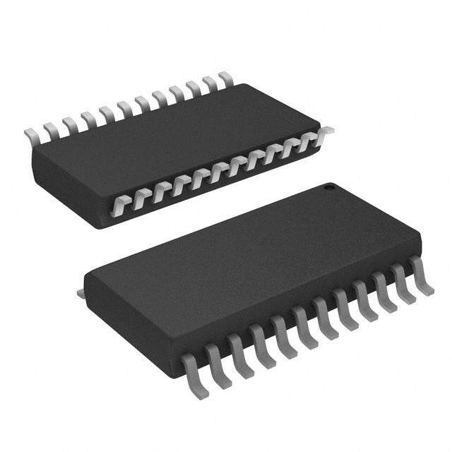
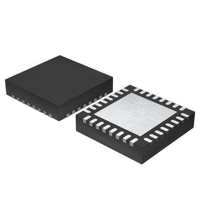
| 描述 | IC ADC 8BIT 40MSPS DL 48-TQFP |
| 产品分类 | |
| 品牌 | Maxim Integrated |
| 数据手册 | |
| 产品图片 |
|
| 产品型号 | MAX1196ECM+D |
| rohs | 无铅 / 符合限制有害物质指令(RoHS)规范要求 |
| 产品系列 | - |
| 产品培训模块 | http://www.digikey.cn/PTM/IndividualPTM.page?site=cn&lang=zhs&ptm=25703http://www.digikey.cn/PTM/IndividualPTM.page?site=cn&lang=zhs&ptm=25705 |
| 位数 | 8 |
| 供应商器件封装 | 48-TQFP-EP (7x7) |
| 其它名称 | MAX1196ECMD |
| 包装 | 托盘 |
| 安装类型 | 表面贴装 |
| 封装/外壳 | 48-TQFP 裸露焊盘 |
| 工作温度 | -40°C ~ 85°C |
| 应用说明 | 点击此处下载产品Datasheet点击此处下载产品Datasheet点击此处下载产品Datasheet点击此处下载产品Datasheet点击此处下载产品Datasheet点击此处下载产品Datasheet |
| 数据接口 | 并联 |
| 标准包装 | 1 |
| 特性 | 同步采样 |
| 电压源 | 单电源 |
| 转换器数 | 2 |
| 输入数和类型 | 4 个单端,双极2 个差分,双极 |
| 采样率(每秒) | 40M |





- 商务部:美国ITC正式对集成电路等产品启动337调查
- 曝三星4nm工艺存在良率问题 高通将骁龙8 Gen1或转产台积电
- 太阳诱电将投资9.5亿元在常州建新厂生产MLCC 预计2023年完工
- 英特尔发布欧洲新工厂建设计划 深化IDM 2.0 战略
- 台积电先进制程称霸业界 有大客户加持明年业绩稳了
- 达到5530亿美元!SIA预计今年全球半导体销售额将创下新高
- 英特尔拟将自动驾驶子公司Mobileye上市 估值或超500亿美元
- 三星加码芯片和SET,合并消费电子和移动部门,撤换高东真等 CEO
- 三星电子宣布重大人事变动 还合并消费电子和移动部门
- 海关总署:前11个月进口集成电路产品价值2.52万亿元 增长14.8%
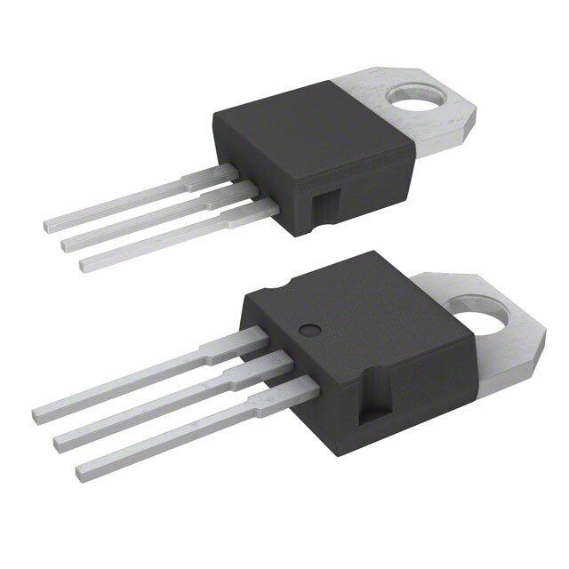
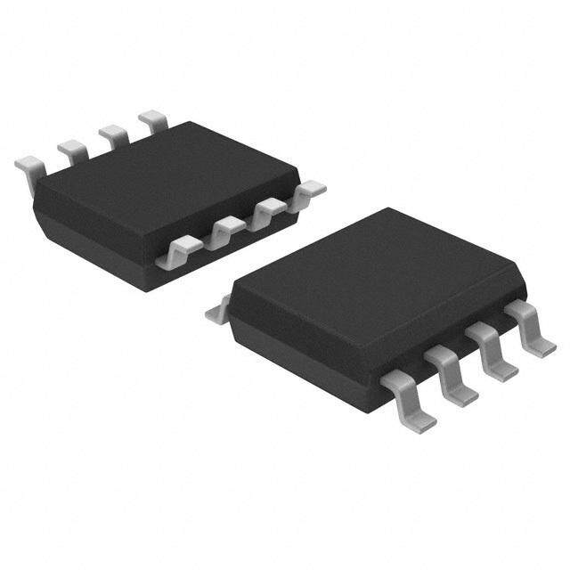
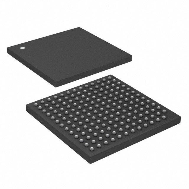

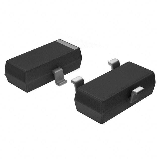
PDF Datasheet 数据手册内容提取
19-2600; Rev 0; 9/02 Dual 8-Bit, 40Msps, 3V, Low-Power ADC with Internal Reference and Multiplexed Parallel Outputs General Description Features M The MAX1196 is a 3V, dual 8-bit analog-to-digital con- (cid:2) Single 2.7V to 3.6V Operation A verter (ADC) featuring fully differential wideband track- (cid:2) Excellent Dynamic Performance X and-hold (T/H) inputs, driving two ADCs. The MAX1196 is optimized for low power, small size, and high-dynamic 48.4dB/44.7dB SINAD at fIN= 20MHz/200MHz 1 performance for applications in imaging, instrumenta- 68.9dB/53dBc SFDR at fIN= 20MHz/200MHz 1 tion, and digital communications. This ADC operates (cid:2) -72dB Interchannel Crosstalk at fIN= 20MHz 9 from a single 2.7V to 3.6V supply, consuming only (cid:2) Low Power 6 87mW while delivering a typical signal-to-noise and dis- tortion (SINAD) of 48.4dB at an input frequency of 87mW (Normal Operation) 20MHz and a sampling rate of 40Msps. The T/H driven 9mW (Sleep Mode) input stages incorporate 400MHz (-3dB) input ampli- 0.3µW (Shutdown Mode) fiers. The converters can also be operated with single- (cid:2) 0.05dB Gain and ±0.05°Phase Matching ended inputs. In addition to low operating power, the MAX1196 features a 3mA sleep mode as well as a (cid:2) Wide ±1VP-PDifferential Analog Input Voltage 0.1µA power-down mode to conserve power during idle Range periods. (cid:2) 400MHz -3dB Input Bandwidth An internal 2.048V precision bandgap reference sets (cid:2) On-Chip 2.048V Precision Bandgap Reference the full-scale range of the ADC. A flexible reference structure allows the use of this internal or an externally (cid:2) User-Selectable Output Format—Two’s applied reference, if desired for applications requiring Complement or Offset Binary increased accuracy or a different input voltage range. (cid:2) Pin-Compatible 8-Bit and 10-Bit Upgrades The MAX1196 features parallel, multiplexed, CMOS- Available compatible three-state outputs. The digital output format Ordering Information can be set to two’s complement or straight offset binary through a single control pin. The device provides for a PART TEMP RANGE PIN-PACKAGE separate output power supply of 1.7V to 3.6V for flexible MAX1196ECM -40°C to +85°C 48 TQFP-EP* interfacing. The MAX1196 is available in a 7mm × 7mm, *EP = Exposed pad. 48-pin TQFP package, and is specified for the extended industrial (-40°C to +85°C) temperature range. Pin Configuration Pin-compatible, nonmultiplexed higher speed versions of tdhaet aM sAhXe1e1t9 f6o ra 1re0 0aMlsosp asv, atihlaeb lMe.A RXe1f1e9r 7to d tahtea MshAeXe1t1 f9o8r REFN REFP REFIN REFOUT D7A/B D6A/B D5A/B D4A/B D3A/B D2A/B D1A/B D0A/B 60Msps, and the MAX1195 data sheet for 40Msps. 48 47 46 45 44 43 42 41 40 39 38 37 For a 10-bit, pin-compatible upgrade, refer to the MAX1186 data sheet. With the N.C. pins of the COM 1 36 N.C. MAX1196 internally pulled down to ground, this ADC VDD 2 35 N.C. becomes a drop-in replacement for the MAX1186. GND 3 34 OGND INA+ 4 33 OVDD Applications INA- 5 32 OVDD Baseband I/Q Sampling VDD 6 MAX1196 31 OGND GND 7 30 A/B Multichannel IF Sampling INB- 8 29 N.C. INB+ 9 28 N.C. Ultrasound and Medical Imaging GND 10 27 N.C. Battery-Powered Instrumentation VDD 11 26 N.C. CLK 12 25 N.C. WLAN, WWAN, WLL, MMDS Modems Set-Top Boxes 13 14 15 16 17 18 19 20 21 22 23 24 VSAT Terminals GND VDDVDDGND T/B LEEP PD OE N.C. N.C. N.C. N.C. S TQFP-EP Functional Diagram appears at end of data sheet. ________________________________________________________________Maxim Integrated Products 1 For pricing, delivery, and ordering information,please contact Maxim/Dallas Direct!at 1-888-629-4642, or visit Maxim’s website at www.maxim-ic.com.
Dual 8-Bit, 40Msps, 3V, Low-Power ADC with Internal Reference and Multiplexed Parallel Outputs 6 ABSOLUTE MAXIMUM RATINGS 9 VDD, OVDDto GND..............................................-0.3V to +3.6V Continuous Power Dissipation (TA= +70°C) 1 OGND to GND......................................................-0.3V to +0.3V 48-Pin TQFP (derate 12.5mW/°C above +70°C)........1000mW 1 INA+, INA-, INB+, INB- to GND...............................-0.3V to VDD Operating Temperature Range...........................-40°C to +85°C REFIN, REFOUT, REFP, REFN, COM, Junction Temperature......................................................+150°C X CLK to GND............................................-0.3V to (VDD+ 0.3V) Storage Temperature Range.............................-60°C to +150°C OE, PD, SLEEP, T/B, Lead Temperature (soldering, 10s).................................+300°C A D7A/B–D0A/B, A/B to OGND...............-0.3V to (OVDD+ 0.3V) M Stresses beyond those listed under “Absolute Maximum Ratings” may cause permanent damage to the device. These are stress ratings only, and functional operation of the device at these or any other conditions beyond those indicated in the operational sections of the specifications is not implied. Exposure to absolute maximum rating conditions for extended periods may affect device reliability. ELECTRICAL CHARACTERISTICS (VDD= OVDD= 3V, 0.1µF and 2.2µF capacitors from REFP, REFN, and COM to GND; REFOUT connected to REFIN through a 10kΩ resistor, VIN = 2VP-P (differential with respect to COM), CL = 10pF at digital outputs (Note 5), fCLK = 40MHz, TA = TMIN to TMAX, unless otherwise noted. ≥+25°C guaranteed by production test, <+25°C guaranteed by design and characterization. Typical values are at TA= +25°C.) PARAMETER SYMBOL CONDITIONS MIN TYP MAX UNITS DC ACCURACY Resolution 8 Bits Integral Nonlinearity INL fIN = 7.51MHz (Note 1) ±0.3 ±1 LSB Differential Nonlinearity DNL fIN = 7.51MHz, no missing codes ±0.15 ±1 LSB guaranteed (Note 1) Offset Error ±4 %FS Gain Error ±4 %FS Gain Temperature Coefficient ±100 ppm/°C ANALOG INPUT Differential Input Voltage Range VDIFF Differential or single-ended inputs ±1.0 V Common-Mode Input Voltage VDD / 2 Range VCM ± 0.2 V Input Resistance RIN Switched capacitor load 140 kΩ Input Capacitance CIN 5 pF CONVERSION RATE Maximum Clock Frequency fCLK 40 MHz CHA 5 Clock Data Latency CHB 5.5 Cycles DYNAMIC CHARACTERISTICS (fCLK = 40MHz) fINA or B = 2MHz at -1dB FS 48.7 fINA or B = 7.5MHz at -1dB FS 48.7 Signal-to-Noise Ratio SNR dB fINA or B = 20MHz at -1dB FS 47.5 48.5 fINA or B = 101MHz at -1dB FS 48 fINA or B = 2MHz at -1dB FS 48.6 fINA or B = 7.5MHz at -1dB FS 48.7 Signal-to-Noise and Distortion SINAD dB fINA or B = 20MHz at -1dB FS 47 48.4 fINA or B = 101MHz at -1dB FS 48 2 _______________________________________________________________________________________
Dual 8-Bit, 40Msps, 3V, Low-Power ADC with Internal Reference and Multiplexed Parallel Outputs ELECTRICAL CHARACTERISTICS (continued) M (VDD= OVDD= 3V, 0.1µF and 2.2µF capacitors from REFP, REFN, and COM to GND; REFOUT connected to REFIN through a 10kΩ A resistor, VIN = 2VP-P (differential with respect to COM), CL = 10pF at digital outputs (Note 5), fCLK = 40MHz, TA = TMIN to TMAX, unless otherwise noted. ≥+25°C guaranteed by production test, <+25°C guaranteed by design and characterization. Typical values X are at TA= +25°C.) 1 PARAMETER SYMBOL CONDITIONS MIN TYP MAX UNITS 1 fINA or B = 2MHz at -1dB FS 69 9 fINA or B = 7.5MHz at -1dB FS 70 6 Spurious-Free Dynamic Range SFDR dBc fINA or B = 20MHz at -1dB FS 60 68.9 fINA or B = 101MHz at -1dB FS 65 fINA or B = 2MHz at -1dB FS -72 fINA or B = 7.5MHz at -1dB FS -73.7 Third-Harmonic Distortion HD3 dBc fINA or B = 20MHz at -1dB FS -75 fINA or B = 101MHz at -1dB FS -67 Intermodulation Distortion fIN1(A or B) = 1.997MHz at -7dB FS, IMD -68 dBc (F irs t Fiv e Odd -O rd er IMD s ) (N o te 2) fIN2(A or B) = 2.046MHz at -7dB FS Third-Order Intermodulation fIN1(A or B) = 1.997MHz at -7dB FS, IM3 -73.2 dBc Distortion (Note 2) fIN2(A or B) = 2.046MHz at -7dB FS fINA or B = 2MHz at -1dB FS -70 Total Harmonic Distortion fINA or B = 7.5MHz at -1dB FS -69 THD dBc (First Four Harmonics) fINA or B = 20MHz at -1dB FS -69 -57 fINA or B = 101MHz at -1dB FS -63 Small-Signal Bandwidth Input at -20dB FS, differential inputs 500 MHz Full-Power Bandwidth FPBW Input at -1dB FS, differential inputs 400 MHz Gain Flatness (12MHz Spacing) fIN1(A or B) = 106MHz at -1dB FS, 0.05 dB (Note 3) fIN2(A or B) = 118MHz at -1dB FS Aperture Delay tAD 1 ns Aperture Jitter tAJ 1dB SNR degradation at Nyquist 2 psRMS Overdrive Recovery Time For 1.5 × full-scale input 2 ns INTERNAL REFERENCE (REFIN = REFOUT through 10kΩ resistor; REFP, REFN, and COM levels are generated internally.) 2.048 Reference Output Voltage VREFOUT (Note 4) ±3% V Positive Reference Output VREFP (Note 5) 2.012 V Voltage Negative Reference Output VREFN (Note 5) 0.988 V Voltage VDD / 2 Common-Mode Level VCOM (Note 5) ± 0.1 V Differential Reference Output 1.024 Voltage Range ∆VREF ∆VREF = VREFP - VREFN ±3% V Reference Temperature TCREF ±100 ppm/°C Coefficient _______________________________________________________________________________________ 3
Dual 8-Bit, 40Msps, 3V, Low-Power ADC with Internal Reference and Multiplexed Parallel Outputs 6 ELECTRICAL CHARACTERISTICS (continued) 9 (VDD= OVDD= 3V, 0.1µF and 2.2µF capacitors from REFP, REFN, and COM to GND; REFOUT connected to REFIN through a 10kΩ 1 resistor, VIN = 2VP-P (differential with respect to COM), CL = 10pF at digital outputs (Note 5), fCLK = 40MHz, TA = TMIN to TMAX, unless otherwise noted. ≥+25°C guaranteed by production test, <+25°C guaranteed by design and characterization. Typical values 1 are at TA= +25°C.) X PARAMETER SYMBOL CONDITIONS MIN TYP MAX UNITS A BUFFERED EXTERNAL REFERENCE (VREFIN = 2.048V) M Positive Reference Output VREFP (Note 5) 2.012 V Voltage Negative Reference Output VREFN (Note 5) 0.988 V Voltage VDD / 2 Common-Mode Level VCOM (Note 5) ±0.1 V Differential Reference Output 1.024 Voltage Range ∆VREF ∆VREF = VREFP - VREFN ±2% V REFIN Resistance RREFIN >50 MΩ Maximum REFP, COM Source ISOURCE 5 mA Current Maximum REFP, CO M Si n k Cu rr e nt ISINK -250 µA Maximum REFN Source Current ISOURCE 250 µA Maximum REFN Sink Current ISINK -5 mA UNBUFFERED EXTERNAL REFERENCE (VREFIN = AGND, reference voltage applied to REFP, REFN, and COM) REFP, REFN Input Resistance RREFP, Measured between REFP and REFN 4 kΩ RREFN REFP, REFN, COM Input CIN 15 pF Capacitance Differential Reference Input 1.024 Voltage Range ∆VREF ∆VREF = VREFP - VREFN ±10% V VDD / 2 COM Input Voltage Range VCOM ±5% V VC O M + REFP Input Voltage VREFP ∆VR EF / 2 V VCOM - REFN Input Voltage VREFN ∆VREF / 2 V DIGITAL INPUTS (CLK, PD, OE, SLEEP, T/B) 0.8 × CLK VDD Input High Threshold VIH V 0.8 × PD, OE, SLEEP, T/B OVDD 0.2 × CLK VDD Input Low Threshold VIL V 0.2 × PD, OE, SLEEP, T/B OVDD 4 _______________________________________________________________________________________
Dual 8-Bit, 40Msps, 3V, Low-Power ADC with Internal Reference and Multiplexed Parallel Outputs ELECTRICAL CHARACTERISTICS (continued) M (VDD= OVDD= 3V, 0.1µF and 2.2µF capacitors from REFP, REFN, and COM to GND; REFOUT connected to REFIN through a 10kΩ A resistor, VIN = 2VP-P (differential with respect to COM), CL = 10pF at digital outputs (Note 5), fCLK = 40MHz, TA = TMIN to TMAX, unless otherwise noted. ≥+25°C guaranteed by production test, <+25°C guaranteed by design and characterization. Typical values X are at TA= +25°C.) 1 PARAMETER SYMBOL CONDITIONS MIN TYP MAX UNITS 1 Input Hysteresis VHYST 0.15 V 9 IIH VIH = VDD = OVDD ±20 6 Input Leakage µA IIL VIL = 0 ±20 Input Capacitance CIN 5 pF DIGITAL OUTPUTS (D0A/B–D7A/B, A/B) Output Voltage Low VOL ISINK = -200µA 0.2 V OVDD - Output Voltage High VOH ISOURCE = 200µA V 0.2 Three-State Leakage Current ILEAK OE = OVDD ±10 µA Three-State Output Capacitance COUT OE = OVDD 5 pF POWER REQUIREMENTS Analog Supply Voltage Range VDD 2.7 3 3.6 V Output Supply Voltage Range OVDD 1.7 3 3.6 V Operating, fINA&B = 20MHz at -1dB FS 29 36 applied to both channels mA Analog Supply Current IVDD Sleep mode 3 Shutdown, clock idle, PD = OE = OVDD 0.1 20 µA Operating, fINA&B = 20MHz at -1dB FS 8 mA applied to both channels (Note 6) Output Supply Current IOVDD Sleep mode 3 µA Shutdown, clock idle, PD = OE = OVDD 3 10 Operating, fINA&B = 20MHz at -1dB FS 87 108 applied to both channels mW Analog Power Dissipation PDISS Sleep mode 9 Shutdown, clock idle, PD = OE = OVDD 0.3 60 µW Offset, VDD ±5% ±3 Power-Supply Rejection PSRR mV/V Gain, VDD ±5% ±3 TIMING CHARACTERISTICS CLK Rise to CHA Output Data tDOA CL = 20pF (Notes 1, 7) 6 8.25 ns Valid CLK Fall to CHB Output Data tDOB CL = 20pF (Notes 1, 7) 6 8.25 ns Valid Clock Rise/Fall to A/B Rise/Fall tDA/B 6 ns Time OE Fall to Output Enable Time tENABLE 5 ns OE Rise to Output Disable Time tDISABLE 5 ns 12.5 CLK Pulse Width High tCH Clock period: 25ns (Note 7) ±1.5 ns _______________________________________________________________________________________ 5
Dual 8-Bit, 40Msps, 3V, Low-Power ADC with Internal Reference and Multiplexed Parallel Outputs 6 ELECTRICAL CHARACTERISTICS (continued) 9 (VDD= OVDD= 3V, 0.1µF and 2.2µF capacitors from REFP, REFN, and COM to GND; REFOUT connected to REFIN through a 10kΩ 1 resistor, VIN = 2VP-P (differential with respect to COM), CL = 10pF at digital outputs (Note 5), fCLK = 40MHz, TA = TMIN to TMAX, unless otherwise noted. ≥+25°C guaranteed by production test, <+25°C guaranteed by design and characterization. Typical values 1 are at TA= +25°C.) X PARAMETER SYMBOL CONDITIONS MIN TYP MAX UNITS A 12.5 M CLK Pulse Width Low tCL Clock period: 25ns (Note 7) ±1.5 ns Wake-up from sleep mode 1 Wake-Up Time tWAKE µs Wake-up from shutdown mode (Note 8) 20 CHANNEL-TO-CHANNEL MATCHING Crosstalk fINA or B = 20MHz at -1dB FS (Note 9) -72 dB Gain Matching fINA or B = 20MHz at -1dB FS (Note 10) 0.05 dB Phase Matching fINA or B = 20MHz at -1dB FS (Note 11) ±0.05 De g re es Note 1: Guaranteed by design. Not subject to production testing. Note 2: Intermodulation distortion is the total power of the intermodulation products relative to the total input power. Note 3: Analog attenuation is defined as the amount of attenuation of the fundamental bin from a converted FFT between two applied input signals with the same magnitude (peak-to-peak) at fIN1and fIN2. Note 4: REFIN and REFOUT should be bypassed to GND with a 0.1µF (min) and 2.2µF (typ) capacitor. Note 5: REFP, REFN, and COM should be bypassed to GND with a 0.1µF (min) and 2.2µF (typ) capacitor. Note 6: Typical digital output current at fINA&B = 20MHz. For digital output currents vs. analog input frequency, see the Typical Operating Characteristics. Note 7: See Figure3 for detailed system timing diagrams. Clock to data valid timing is measured from 50% of the clock level to 50% of the data output level. Note 8: SINAD settles to within 0.5dB of its typical value in unbuffered external reference mode. Note 9: Crosstalk rejection is tested by applying a test tone to one channel and holding the other channel at DC level. Crosstalk is measured by calculating the power ratio of the fundamental of each channel’s FFT. Note 10:Amplitude matching is measured by applying the same signal to each channel and comparing the magnitude of the funda- mental of the calculated FFT. Note 11:Phase matching is measured by applying the same signal to each channel and comparing the phase of the fundamental of the calculated FFT. The data from both ADC channels must be captured simultaneously during this test. 6 _______________________________________________________________________________________
Dual 8-Bit, 40Msps, 3V, Low-Power ADC with Internal Reference and Multiplexed Parallel Outputs Typical Operating Characteristics M (VDD= OVDD= 3V, VREFIN= 2.048V, differential input at -1dB FS, fCLK= 40MHz, CL≈10pF, TA= +25°C, unless otherwise noted.) A X FFT PLOT CHA FFT PLOT CHB FFT PLOT CHA (DIFFERENTIAL INPUT, 8192-POINT DATA RECORD) (DIFFERENTIAL INPUT, 8192-POINT DATA RECORD) (DIFFERENTIAL INPUT, 8192-POINT DATA RECORD) 1 --21000 fINA fffCIINNLABK === 174..095.530840020385676MM78HHMzzHz MAX1196-01 --21000 fffCIINNLABK === 174..095.530840020385676MM78HHMzzHz MAX1196-02 --21000 fINA fffCIINNLABK === 714..059.350480200835766MM78HHMzzHz MAX1196-03 196 AINA = AINB = -1dB FS AINA = AINB = -1dB FS AINA = AINB = -1dB FS DE (dB) --4300 COHERENT SAMPLING DE (dB) --4300 fINB COHERENT SAMPLING DE (dB) --4300 COHERENT SAMPLING U U U MPLIT -50 HD2 HD3 fINB MPLIT -50 HD3 MPLIT -50 A -60 A -60 fINA HD2 A -60 fINB HD2 HD3 -70 -70 -70 -80 -80 -80 -90 -90 -90 0 2 4 6 8 10 12 14 16 18 20 0 2 4 6 8 10 12 14 16 18 20 0 2 4 6 8 10 12 14 16 18 20 ANALOG INPUT FREQUENCY (MHz) ANALOG INPUT FREQUENCY (MHz) ANALOG INPUT FREQUENCY (MHz) FFT PLOT CHB FFT PLOT CHA FFT PLOT CHB (DIFFERENTIAL INPUT, 8192-POINT DATA RECORD) (DIFFERENTIAL INPUT, 8192-POINT DATA RECORD) (DIFFERENTIAL INPUT, 8192-POINT DATA RECORD) --21000 fINB fffACIINNILNABKA === = 714 ..A059I.35N0480B200 83=576 6-MM17d8HHBMzz FHSz MAX1196-04 --21000 fffACIINNILNABKA === = 144 90A0..I.84N0890B730 97=584 6-MM17d8HHBMzz FHSz MAX1196-05 --21000 fINB fffACIINNILNABKA === = 144 90A0..I.84N0890B730 97=584 6-MM17d8HHBMzz FHSz MAX1196-06 B) -30 COHERENT SAMPLING B) -30 COHERENT SAMPLING B) -30 COHERENT SAMPLING DE (d -40 DE (d -40 fINA DE (d -40 MPLITU -50 HD3 MPLITU -50 HD2 MPLITU -50 HD2 A -60 HD2 fINA A -60 fINB HD3 A -60 HD3 fINA -70 -70 -70 -80 -80 -80 -90 -90 -90 0 2 4 6 8 10 12 14 16 18 20 0 2 4 6 8 10 12 14 16 18 20 0 2 4 6 8 10 12 14 16 18 20 ANALOG INPUT FREQUENCY (MHz) ANALOG INPUT FREQUENCY (MHz) ANALOG INPUT FREQUENCY (MHz) FFT PLOT CHA FFT PLOT CHB TWO-TONE IMD PLOT (DIFFERENTIAL INPUT, 8192-POINT DATA RECORD) (DIFFERENTIAL INPUT, 8192-POINT DATA RECORD) (DIFFERENTIAL INPUT, 8192-POINT DATA RECORD) -100 ffCINLAK == 4400..4090307546M78HMzHz MAX1196-07 -100 ffCINLAK == 4400..4090307546M78HMzHz MAX1196-08 -100 ffCINLAK == 14.09.9070114573M6MHzHz MAX1196-09 -20 fINB = 19.88798MHz -20 fINB = 19.88798MHz -20 fINB = 2.045977MHz fINA AINA = AINB = -1dB FS AINA = AINB = -1dB FS AIN = -7dB FS AMPLITUDE (dB) ----65430000 HD2 HD3 COHERENT SAMfPINLBING AMPLITUDE (dB) ----65430000 HCDO2HERENfITN ASAMPLING HD3fINB AMPLITUDE (dB) ----65430000 fIN1 fIN2 COHERENT SAMPLING -70 -70 -70 -80 -80 -80 -90 -90 -90 0 2 4 6 8 10 12 14 16 18 20 0 2 4 6 8 10 12 14 16 18 20 0.5 1.0 1.5 2.0 2.5 3.0 3.5 4.0 4.5 5.0 ANALOG INPUT FREQUENCY (MHz) ANALOG INPUT FREQUENCY (MHz) ANALOG INPUT FREQUENCY (MHz) _______________________________________________________________________________________ 7
Dual 8-Bit, 40Msps, 3V, Low-Power ADC with Internal Reference and Multiplexed Parallel Outputs 6 Typical Operating Characteristics (continued) 9 (VDD= OVDD= 3V, VREFIN= 2.048V, differential input at -1dB FS, fCLK= 40MHz, CL≈10pF, TA= +25°C, unless otherwise noted.) 1 1 TWO-TONE IMD PLOT SIGNAL-TO-NOISE RATIO SIGNAL-TO-NOISE + DISTORTION X (DIFFERENTIAL INPUT, 8192-POINT DATA RECORD) vs. ANALOG INPUT FREQUENCY vs. ANALOG INPUT FREQUENCY MA --21000 fffCIINNL12K == = 91 4.090.50.0620441375M9396HMMzHHzz MAX1196-10 4590 CHB MAX1196-11 4590 CHB MAX1196-12 AIN = -7dB FS 48 B) -30 COHERENT SAMPLING 48 AMPLITUDE (d ---654000 fIN1 fIN2 SNR (dB) 4467 SINAD (dB) 4467 CHA CHA 45 -70 45 44 -80 -90 44 43 7 8 9 10 11 12 13 0 40 80 120 160 200 0 40 80 120 160 200 ANALOG INPUT FREQUENCY (MHz) ANALOG INPUT FREQUENCY (MHz) ANALOG INPUT FREQUENCY (MHz) TOTAL HARMONIC DISTORTION SPURIOUS-FREE DYNAMIC RANGE FULL-POWER INPUT BANDWIDTH vs. ANALOG INPUT FREQUENCY vs. ANALOG INPUT FREQUENCY vs. ANALOG INPUT FREQUENCY, DIFFERENTIAL --4388 MAX1196-13 8900 MAX1196-14 21 MAX1196-15 CHB CHA 0 THD (dBc) --6588 SFDR (dBc) 6700 CHA GAIN (dB) -1 CHB -2 -78 50 -3 -88 40 -4 0 40 80 120 160 200 0 40 80 120 160 200 1 10 100 1000 ANALOG INPUT FREQUENCY (MHz) ANALOG INPUT FREQUENCY (MHz) ANALOG INPUT FREQUENCY (MHz) SMALL-SIGNAL INPUT BANDWIDTH SIGNAL-TO-NOISE RATIO SIGNAL-TO-NOISE + DISTORTION vs. ANALOG INPUT FREQUENCY, DIFFERENTIAL vs. INPUT POWER (fIN = 19.88798MHz) vs. INPUT POWER (fIN = 19.88798MHz) 21 VIN = 100mVP-P MAX1196-16 5505 MAX1196-17 5505 MAX1196-18 0 45 45 GAIN (dB) -1 SNR (dB) 40 SINAD (dB) 40 -2 35 35 -3 30 30 -4 25 25 1 10 100 1000 -20 -16 -12 -8 -4 0 -20 -16 -12 -8 -4 0 ANALOG INPUT FREQUENCY (MHz) INPUT POWER (dB FS) INPUT POWER (dB FS) 8 _______________________________________________________________________________________
Dual 8-Bit, 40Msps, 3V, Low-Power ADC with Internal Reference and Multiplexed Parallel Outputs Typical Operating Characteristics (continued) M (VDD= OVDD= 3V, VREFIN= 2.048V, differential input at -1dB FS, fCLK= 40MHz, CL≈10pF, TA= +25°C, unless otherwise noted.) A X TOTAL HARMONIC DISTORTION SPURIOUS-FREE DYNAMIC RANGE SNR/SINAD, THD/SFDR 1 vs. INPUT POWER (fIN = 19.88798MHz) vs. INPUT POWER (fIN = 19.88798MHz) vs. CLOCK DUTY CYCLE 1 --5405 MAX1196-19 6772 MAX1196-20 Bc) 7800 fINA/B = 7.534287MHz SFDR MAX1196-21 96 d B, SINAD (dBc) --6505 SFDR (dBc) 5672 D, THD/SFDR (d 5600 SNR THD A -65 52 SIN R/ SN 40 SINAD -70 47 -75 42 30 -20 -16 -12 -8 -4 0 -20 -16 -12 -8 -4 0 40 44 48 52 56 60 INPUT POWER (dB FS) INPUT POWER (dB FS) CLOCK DUTY CYCLE (%) INTEGRAL NONLINEARITY DIFFERENTIAL NONLINEARITY (131,072-POINT DATA RECORD) (131,072-POINT DATA RECORD) 000...345 fIN = 7.534287MHz MAX1196-22 000...345 fIN = 7.534287MHz MAX1196-23 0.2 0.2 B) 0.1 B) 0.1 S S NL (L 0 NL (L 0 I -0.1 D -0.1 -0.2 -0.2 -0.3 -0.3 -0.4 -0.4 -0.5 -0.5 0 32 64 96 128 160 192 224 256 0 32 64 96 128 160 192 224 256 DIGITAL OUTPUT CODE DIGITAL OUTPUT CODE GAIN ERROR vs. TEMPERATURE, OFFSET ERROR vs. TEMPERATURE, EXTERNAL REFERENCE VREFIN = 2.048V EXTERNAL REFERENCE VREFIN = 2.048V 0.5 0.2 0.4 MAX1196-24 MAX1196-25 0 CHA FS) 0.3 CHB %FS) R (% OR ( -0.2 RO 0.2 RR GAIN ER 0.1 FFSET E -0.4 O CHB -0.6 0 CHA -0.1 -0.8 -40 -15 10 35 60 85 -40 -15 10 35 60 85 TEMPERATURE (°C) TEMPERATURE (°C) _______________________________________________________________________________________ 9
Dual 8-Bit, 40Msps, 3V, Low-Power ADC with Internal Reference and Multiplexed Parallel Outputs 6 Typical Operating Characteristics (continued) 9 (VDD= OVDD= 3V, VREFIN= 2.048V, differential input at -1dB FS, fCLK= 40MHz, CL≈10pF, TA= +25°C, unless otherwise noted.) 1 1 X ANALOG SUPPLY CURRENT DIGITAL SUPPLY CURRENT INTERNAL REFERENCE VOLTAGE vs. TEMPERATURE vs. ANALOG INPUT FREQUENCY vs. ANALOG SUPPLY VOLTAGE MA 3323 MAX1196-26 8 MAX1196-27 22..00332204 MAX1196-28 7 31 2.0316 I (mA)VDD 223890 I (mA)OVDD 56 V (V)REFOUT2.0312 2.0308 27 4 2.0304 26 25 3 2.0300 -40 -15 10 35 60 85 0 4 8 12 16 20 2.70 2.85 3.00 3.15 3.30 3.45 3.60 TEMPERATURE (°C) ANALOG INPUT FREQUENCY (MHz) VDD (V) INTERNAL REFERENCE VOLTAGE SNR/SINAD, THD/SFDR vs. TEMPERATURE vs. SAMPLING SPEED 22..003460 MAX1196-29 Bc) 1680000 SNR SFDR fIN = 20MHz MAX1196-30 d dB, 40 R ( SINAD V (V)REFOUT22..002382 D, THD/SFD -22000 NA THD SI -40 R/ 2.024 SN -60 -80 2.020 -100 -40 -15 10 35 60 85 0 10 20 30 40 50 60 TEMPERATURE (°C) SAMPLING SPEED (Msps) Pin Description PIN NAME FUNCTION 1 COM Common-Mode Voltage Input/Output. Bypass to GND with a ≥0.1µF capacitor. 2, 6, 11, 14, 15 VDD Analog Supply Voltage. Bypass to GND with a capacitor combination of 2.2µF in parallel with 0.1µF. 3, 7, 10, 13, 16 GND Analog Ground 4 INA+ Channel ‘A’ Positive Analog Input. For single-ended operation, connect signal source to INA+. 5 INA- Channel ‘A’ Negative Analog Input. For single-ended operation, connect INA- to COM. 8 INB- Channel ‘B’ Negative Analog Input. For single-ended operation, connect INB- to COM. 9 INB+ Channel ‘B’ Positive Analog Input. For single-ended operation, connect signal source to INB+. 12 CLK Converter Clock Input 10 ______________________________________________________________________________________
Dual 8-Bit, 40Msps, 3V, Low-Power ADC with Internal Reference and Multiplexed Parallel Outputs Pin Description (continued) M PIN NAME FUNCTION A X T/B selects the ADC digital output format. 17 T/B High: Two’s complement. 1 Low: Straight offset binary. 1 Sleep Mode Input. 9 18 SLEEP High: Deactivates the two ADCs, but leaves the reference bias circuit active. 6 Low: Normal operation. High-Active Power-Down Input. 19 PD High: Power-down mode Low: Normal operation Low-Active Output Enable Input. 20 OE High: Digital outputs disabled Low: Digital outputs enabled 21–29, 35, 36 N.C. No Connection. Do not connect. A/B Data Indicator. This digital output indicates CHA data (A/B = 1) or CHB data (A/B = 0) to be 30 A/B present on the output. A/B follows the external clock signal with typically 6ns delay. 31, 34 OGND Output-Driver Ground Output-Driver Supply Voltage. Bypass to OGND with a capacitor combination of 2.2µF in parallel with 32, 33 OVDD 0.1µF. Three-State Digital Output, Bit 0. Depending on status of A/B, output data reflects channel A or 37 D0A/B channel B data. Three-State Digital Output, Bit 1. Depending on status of A/B, output data reflects channel A or 38 D1A/B channel B data. Three-State Digital Output, Bit 2. Depending on status of A/B, output data reflects channel A or 39 D2A/B channel B data. Three-State Digital Output, Bit 3. Depending on status of A/B, output data reflects channel A or 40 D3A/B channel B data. Three-State Digital Output, Bit 4. Depending on status of A/B, output data reflects channel A or 41 D4A/B channel B data. Three-State Digital Output, Bit 5. Depending on status of A/B, output data reflects channel A or 42 D5A/B channel B data. Three-State Digital Output, Bit 6. Depending on status of A/B, output data reflects channel A or 43 D6A/B channel B data. Three-State Digital Output, Bit 7 (MSB). Depending on status of A/B, output data reflects channel A or 44 D7A/B channel B data. 45 REFOUT Internal Reference Voltage Output. Can be connected to REFIN through a resistor or a resistor-divider. 46 REFIN Reference Input. VREFIN = 2 × (VREFP - VREFN). Bypass to GND with a ≥0.1µF capacitor. 47 REFP Positive Reference I/O. Conversion range is ±(VREFP - VREFN). Bypass to GND with a ≥0.1µF capacitor. Negative Reference I/O. Conversion range is ±(VREFP - VREFN). Bypass to GND with a ≥0.1µF 48 REFN capacitor. ______________________________________________________________________________________ 11
Dual 8-Bit, 40Msps, 3V, Low-Power ADC with Internal Reference and Multiplexed Parallel Outputs 6 9 2-BIT FLASH 2-BIT FLASH 1 ADC ADC 1 X STAGE 1 STAGE 2 STAGE 6 STAGE 7 STAGE 1 STAGE 2 STAGE 6 STAGE 7 A M DIGITAL ALIGNMENT LOGIC DIGITAL ALIGNMENT LOGIC T/H 8 T/H 8 VINA VINB OUTPUT MULTIPLEXER 8 D0A/B–D7A/B Figure1. Pipelined Architecture—Stage Blocks Detailed Description S4b, S5a, and S5b are closed. The fully differential cir- cuits sample the input signals onto the two capacitors The MAX1196 uses a 7-stage, fully differential, pipelined (C2a and C2b) through switches S4a and S4b. S2a and architecture (Figure 1) that allows for high-speed con- S2b set the common mode for the amplifier input, and version while minimizing power consumption. Samples open simultaneously with S1, sampling the input wave- taken at the inputs move progressively through the form. Switches S4a, S4b, S5a, and S5b are then pipeline stages every half clock cycle. Including the opened before switches S3a and S3b connect capaci- delay through the output latch, the total clock-cycle tors C1a and C1b to the output of the amplifier and latency is 5 clock cycles for CHA and 5.5 clock cycles switch S4c is closed. The resulting differential voltages for CHB. are held on capacitors C2a and C2b. The amplifiers are Flash ADCs convert the held input voltages into a digi- used to charge capacitors C1a and C1b to the same tal code. Internal MDACs convert the digitized results values originally held on C2a and C2b. These values back into analog voltages, which are then subtracted are then presented to the first stage quantizers and iso- from the original held input signals. The resulting error late the pipelines from the fast-changing inputs. The signals are then multiplied by two, and the residues are wide input bandwidth T/H amplifiers allow the MAX1196 passed along to the next pipeline stages where the to track and sample/hold analog inputs of high frequen- process is repeated until the signals have been cies (>Nyquist). Both ADC inputs (INA+, INB+, INA-, processed by all 7 stages. and INB-) can be driven either differentially or single Both input channels are sampled on the rising edge of ended. Match the impedance of INA+ and INA-, as well the clock and the resulting data is multiplexed at the as INB+ and INB-, and set the common-mode voltage output. CHA data is updated on the rising edge (5 to midsupply (VDD/2) for optimum performance. clock cycles later) and CHB data is updated on the Analog Inputs and Reference falling edge (5.5 clock cycles later) of the clock signal. Configurations The A/B indicator follows the clock signal with a typical The full-scale range of the MAX1196 is determined by delay time of 6ns and remains high when CHA data is the internally generated voltage difference between updated and low when CHB data is updated. REFP (VDD/2 + VREFIN/4) and REFN (VDD/2 - VREFIN/4). Input Track-and-Hold (T/H) Circuits The full-scale range for both on-chip ADCs is Figure 2 displays a simplified functional diagram of the adjustable through the REFIN pin, which is provided for input track-and-hold (T/H) circuits in both track and this purpose. hold mode. In track mode, switches S1, S2a, S2b, S4a, 12 ______________________________________________________________________________________
Dual 8-Bit, 40Msps, 3V, Low-Power ADC with Internal Reference and Multiplexed Parallel Outputs M INTERNAL BIAS COM A X S2a S5a C1a S3a 1 1 S4a 9 INA+ 6 OUT C2a S4c S1 OUT INA- S4b C2b C1b S3b S2b S5b INTERNAL COM CLK BIAS HOLD HOLD INTERNAL INTERNAL BIAS COM TRACK TRACK NONOVERLAPPING CLOCK SIGNALS S2a S5a C1a S3a S4a INB+ OUT C2a S4c S1 MAX1196 OUT INB- S4b C2b C1b S3b S2b S5b INTERNAL COM BIAS Figure2. MAX1196 T/H Amplifiers The MAX1196 provides three modes of reference 10kΩ) or resistor-divider, if an application requires a operation: reduced full-scale range. For stability and noise-filtering • Internal reference mode purposes, bypass REFIN with a ≥0.1µF capacitor to GND. In internal reference mode, REFOUT, COM, • Buffered external reference mode REFP, and REFN become low-impedance outputs. • Unbuffered external reference mode In buffered external reference mode, adjust the refer- In internal reference mode, connect the internal refer- ence voltage levels externally by applying a stable and ence output REFOUT to REFIN through a resistor (e.g., accurate voltage at REFIN. In this mode, COM, REFP, ______________________________________________________________________________________ 13
Dual 8-Bit, 40Msps, 3V, Low-Power ADC with Internal Reference and Multiplexed Parallel Outputs 6 and REFN are outputs. REFOUT can be left open or Clock jitter is especially critical for undersampling connected to REFIN through a >10kΩresistor. applications. The clock input should always be consid- 9 ered as an analog input and routed away from any ana- 1 In unbuffered external reference mode, connect REFIN log input or other digital signal lines. to GND. This deactivates the on-chip reference buffers 1 for REFP, COM, and REFN. With their buffers shut down, The MAX1196 clock input operates with a voltage X these nodes become high-impedance inputs and can be threshold set to VDD/2. Clock inputs with a duty cycle A driven through separate, external reference sources. other than 50%, must meet the specifications for high and low periods as stated in the Electrical M For detailed circuit suggestions and how to drive this Characteristics. dual ADC in buffered/unbuffered external reference mode, see the Applications Informationsection. System Timing Requirements Clock Input (CLK) Figure 3 shows the relationship between clock and analog input, A/B indicator, and the resulting valid The MAX1196’s CLK input accepts CMOS-compatible CHA/CHB data output. CHA and CHB data are sam- clock signal. Since the interstage conversion of the pled on the rising edge of the clock signal. Following device depends on the repeatability of the rising and the rising edge of the 5th clock cycles, the digitized falling edges of the external clock, use a clock with low value of the original CHA sample is presented at the jitter and fast rise and fall times (<2ns). In particular, output, followed one-half clock cycle later by the digi- sampling occurs on the rising edge of the clock signal, tized value of the original CHB sample. requiring this edge to provide lowest possible jitter. Any significant aperture jitter would limit the SNR perfor- A channel selection signal (A/B indicator) allows the mance of the on-chip ADCs as follows: user to determine which output data represents which input channel. With A/B = 1, digitized data from CHA is 1 present at the output and with A/B = 0 digitized data SNR = 20 × log 2×π×f ×t from CHB is present. IN AJ where fIN represents the analog input frequency and tAJis the time of the aperture jitter. 5 CLOCK-CYCLE LATENCY (CHA), 5.5 CLOCK-CYCLE LATENCY (CHB) CHA CHB tCLK tCL tCH CLK tDOB tDOA A/B CHB CHA CHB CHA CHB CHA CHB CHA CHB CHA CHB CHA CHB tDA/B D0A/B–D7A/B D0B D1A D1B D2A D2B D3A D3B D4A D4B D5A D5B D6A D6B Figure3. System Timing Diagram 14 ______________________________________________________________________________________
Dual 8-Bit, 40Msps, 3V, Low-Power ADC with Internal Reference and Multiplexed Parallel Outputs Digital Output Data, Output Data Format Power-Down (PD) and Sleep M Selection (T/B), Output Enable (OE), (SLEEP) Modes Channel Selection (A/B) The MAX1196 offers two power-save modes—sleep A All digital outputs, D0A/B–D7A/B (CHA or CHB data) and and full power-down mode. In sleep mode (SLEEP = 1), X A/B are TTL/CMOS-logic compatible. The output coding only the reference bias circuit is active (both ADCs are 1 can be chosen to be either offset binary or two’s comple- disabled), and current consumption is reduced to 3mA. 1 ment (Table 1) controlled by a single pin (T/B). Pull T/B To enter full power-down mode, pull PD high. With OE low to select offset binary and high to activate two’s com- 9 simultaneously low, all outputs are latched at the last plement output coding. The capacitive load on the digital 6 value prior to the power down. Pulling OE high forces outputs D0A/B–D7A/B should be kept as low as possible the digital outputs into a high-impedance state. (<15pF), to avoid large digital currents that could feed back into the analog portion of the MAX1196, thereby Applications Information degrading its dynamic performance. Using buffers on Figure 5 depicts a typical application circuit containing the digital outputs of the ADCs can further isolate the two single-ended-to-differential converters. The internal digital outputs from heavy capacitive loads. To further reference provides a VDD/2 output voltage for level-shift- improve the dynamic performance of the MAX1196, ing purposes. The input is buffered and then split to a small-series resistors (e.g., 100Ω) can be added to the voltage follower and inverter. One lowpass filter per digital output paths, close to the MAX1196. amplifier suppresses some of the wideband noise asso- Figure 4 displays the timing relationship between out- ciated with high-speed operational amplifiers. The user put enable and data output valid as well as power- can select the RISO and CIN values to optimize the filter down/wake-up and data output valid. performance, to suit a particular application. For the application in Figure 5, an RISO of 50Ω is placed before the capacitive load to prevent ringing and oscillation. The 22pF CINcapacitor acts as a small filter capacitor. OE Using Transformer Coupling An RF transformer (Figure 6) provides an excellent solu- tENABLE tDISABLE tion to convert a single-ended source signal to a fully dif- ferential signal, required by the MAX1196 for optimum OUTPUT HIGH-Z HIGH-Z performance. Connecting the center tap of the trans- D0A/B–D7A/B VALID DATA former to COM provides a VDD/2 DC level shift to the input. Although a 1:1 transformer is shown, a step-up transformer can be selected to reduce the drive require- Figure4. Output Timing Diagram ments. A reduced signal swing from the input driver, such as an op amp, can also improve the overall distortion. Table 1. MAX1196 Output Codes for Differential Inputs STRAIGHT OFFSET DIFFERENTIAL INPUT TWO’S COMPLEMENT DIFFERENTIAL INPUT BINARY VOLTAGE* T/B = 1 T/B = 0 VREF × 255/256 +Full Scale - 1LSB 1111 1111 0111 1111 VREF × 1/256 +1LSB 1000 0001 0000 0001 0 Bipolar Zero 1000 0000 0000 0000 -VREF × 1/256 -1LSB 0111 1111 1111 1111 -VREF × 255/256 -Full Scale + 1LSB 0000 0001 1000 0001 -VREF × 256/256 -Full Scale 0000 0000 1000 0000 *VREF= VREFP- VREFN ______________________________________________________________________________________ 15
Dual 8-Bit, 40Msps, 3V, Low-Power ADC with Internal Reference and Multiplexed Parallel Outputs 6 +5V 9 1 0.1µF 1 LOWPASS FILTER X INA- MAX4108 A 330000ΩΩ 0.1µF R50ISΩ0 CIN 22pF M 0.1µF -5V 600Ω 600Ω +5V 300Ω COM 0.1µF +5V 0.1µF 600Ω INPUT 0.1µF LOWPASS FILTER MAX4108 300Ω MAX4108 INA+ 0.1µF R50ISΩ0 C22INpF -5V 300Ω -5V 0.1µF 300Ω 300Ω +5V 600Ω MAX1196 0.1µF LOWPASS FILTER INB- MAX4108 300Ω 0.1µF R50ISΩ0 CIN 22pF 0.1µF -5V +5V 600Ω 600Ω 300Ω 0.1µF 0.1µF +5V INPUT 600Ω 0.1µF LOWPASS FILTER MAX4108 300Ω INB+ MAX4108 0.1µF R50ISΩ0 C22INpF -5V 300Ω -5V 0.1µF 300Ω 300Ω 600Ω Figure5. Typical Application for Single-Ended-to-Differential Conversion 16 ______________________________________________________________________________________
Dual 8-Bit, 40Msps, 3V, Low-Power ADC with Internal Reference and Multiplexed Parallel Outputs In general, the MAX1196 provides better SFDR and Buffered External Reference Drives M THD with fully differential input signals than single- Multiple ADCs ended drive, especially for very high input frequencies. Multiple-converter systems based on the MAX1196 are A In differential input mode, even-order harmonics are well suited for use with a common reference voltage. X lower as both inputs (INA+, INA- and/or INB+, INB-) are The REFIN pin of those converters can be connected 1 balanced, and each of the ADC inputs only requires directly to an external reference source. half the signal swing compared to single-ended mode. 1 A precision bandgap reference like the MAX6062 gen- 9 Single-Ended AC-Coupled Input Signal erates an external DC level of 2.048V (Figure 8), and Figure 7 shows an AC-coupled, single-ended applica- exhibits a noise voltage density of 150nV/√Hz. Its out- 6 tion. Amplifiers like the MAX4108 provide high speed, put passes through a one-pole lowpass filter (with 10Hz high bandwidth, low noise, and low distortion to main- cutoff frequency) to the MAX4250, which buffers the tain the integrity of the input signal. reference before its output is applied to a second 10Hz lowpass filter. The MAX4250 provides a low offset volt- age (for high gain accuracy) and a low noise level. The passive 10Hz filter following the buffer attenuates noise 25Ω REFP INA+ 22pF 0.1µF VIN 0.1µF 1kΩ R50ISΩO 1 T1 6 INA+ VIN MAX4108 CIN 2 5 100Ω 1kΩ 22pF N.C. COM 2.2µF 0.1µF COM 3 4 REFN 0.1µF MINICIRCUITS RISO TT1-6-KK81 50Ω 25Ω INA- 100Ω INA- CIN 22pF 22pF MAX1196 25Ω REFP MAX1196 INB+ 22pF 0.1µF VIN 0.1µF 1kΩ R50ISΩO 1 T1 6 INB+ VIN MAX4108 CIN 2 5 100Ω 1kΩ 22pF N.C. 2.2µF 0.1µF 3 4 REFN 0.1µF MINICIRCUITS RISO TT1-6-KK81 50Ω 25Ω INB- 100Ω INB- CIN 22pF 22pF Figure6. Transformer-Coupled Input Drive Figure7. Using an Op Amp for Single-Ended, AC-Coupled Input Drive ______________________________________________________________________________________ 17
Dual 8-Bit, 40Msps, 3V, Low-Power ADC with Internal Reference and Multiplexed Parallel Outputs 6 9 3.3V 1 0.1µF 3.3V 1 N.C. 29 0.1µF 2.048V REFOUT X 31 1 REFIN A 0.1µF 32 REFP M 2 16.2kΩ 3 5 1 REFN N = 1 MAX6062 162Ω 2 COM 1 MAX1196 1µF MAX4250 4 3 100µF 10Hz LOWPASS 2 0.1µF 0.1µF 0.1µF FILTER 10Hz LOWPASS FILTER NOTE: ONE FRONT-END REFERENCE CIRCUIT DESIGN CAN BE USED WITH UP TO 1000 ADCs. 0.1µF 2.2µF 10V N.C. 29 REFOUT 31 REFIN 0.1µF 32 REFP N = 1000 1 REFN MAX1196 2 COM 0.1µF 0.1µF 0.1µF Figure8. External Buffered (MAX4250) Reference Drive Using a MAX6062 Bandgap Reference produced in the voltage-reference and buffer stages. ual voltage followers are connected to 10Hz lowpass fil- This filtered noise density, which decreases for higher ters, which filter both the reference-voltage and amplifier frequencies, meets the noise levels specified for preci- noise to a level of 3nV/√Hz. The 2.0V and 1.0V reference sion-ADC operation. voltages set the differential full-scale range of the asso- ciated ADCs at 2VP-P. The 2.0V and 1.0V buffers drive Unbuffered External Reference Drives the ADCs’ internal ladder resistances between them. Multiple ADCs Connecting each REFIN to analog ground disables the Note that the common power supply for all active com- internal reference of each device, allowing the internal ponents removes any concern regarding power-supply reference ladders to be driven directly by a set of exter- sequencing when powering up or down. nal reference sources. Followed by a 10Hz lowpass fil- With the outputs of the MAX4252 matching better than ter and precision voltage-divider, the MAX6066 0.1%, the buffers and subsequent lowpass filters can generates a DC level of 2.500V. The buffered outputs of be replicated to support as many as 32 ADCs. For this divider are set to 2.0V, 1.5V, and 1.0V, with an applications requiring more than 32 matched ADCs, a accuracy that depends on the tolerance of the divider voltage-reference and divider string common to all con- resistors. verters is highly recommended. Those three voltages are buffered by the MAX4252, which provides low noise and low DC offset. The individ- 18 ______________________________________________________________________________________
Dual 8-Bit, 40Msps, 3V, Low-Power ADC with Internal Reference and Multiplexed Parallel Outputs M A 3.3V X 0.1µF N.C. 29 1 REFOUT 31 1 1 REFIN 2.0V 3.3V 32 REFP 9 MAX6066 2 21.5kΩ 3 4 1/4 MAX4252 2.0V AT 8mA 1 REFN N = 1 6 47kΩ 1 MAX1196 2 2 COM 3 11 10µF 330µF 21.5kΩ 6V 6V 1.47kΩ 0.1µF 0.1µF 0.1µF 1.5V 3.3V 4 5 1/4 MAX4252 1.5V AT 0mA 47kΩ 7 6 1µF 11 10µF 330µF 21.5kΩ 6V1.47kΩ 6V 0.1µF 2.2µF 10V 3.3V 1.0V 3.3V 0.1µF 10 4 1/4 MAX4252 1.0V AT -8mA 47kΩ 8 21.5kΩ 9 MBYAPXA4S2S5I4N PGO. WPLEARC-SE UCPAPPLAYC ITOR 21.5kΩ 11 160Vµ1F.47kΩ 330µ6VF N.C. 2391 RREEFFOINUT AS CLOSE AS POSSIBLE TO 32 N = 32 THE OP AMP. REFP 1 REFN MAX1196 2 COM NOTE: ONE FRONT-END REFERENCE CIRCUIT DESIGN CAN BE USED WITH UP TO 32 ADCs. 0.1µF 0.1µF 0.1µF Figure9. External Unbuffered Reference Drive With MAX4252 and MAX6066 Typical QAM Demodulation Application component, where the Q component is 90 degrees A frequently used modulation technique in digital com- phase-shifted with respect to the in-phase component. munications applications is quadrature amplitude mod- At the receiver, the QAM signal is divided down into its ulation (QAM). Typically found in spread- spectrum- I and Q components, essentially representing the mod- based systems, a QAM signal represents a carrier fre- ulation process reversed. Figure 10 displays the quency modulated in both amplitude and phase. At the demodulation process performed in the analog domain, transmitter, modulating the baseband signal with quad- using the dual matched 3V, 8-bit ADC MAX1196, and rature outputs, a local oscillator followed by subse- the MAX2451 quadrature demodulator to recover and quent up-conversion can generate the QAM signal. The digitize the I and Q baseband signals. Before being result is an in-phase (I) and a quadrature (Q) carrier digitized by the MAX1196, the mixed-down signal com- ponents can be filtered by matched analog filters, such ______________________________________________________________________________________ 19
Dual 8-Bit, 40Msps, 3V, Low-Power ADC with Internal Reference and Multiplexed Parallel Outputs 6 9 A/B 1 MAX2451 INA+ 1 INA- X A 0° 90° DSP M MAX1196 POST- PROCESSING INB+ INB- CHA AND CHB DATA DOWNCONVERTER ALTERNATINGLY ÷8 AVAILABLE ON 8-BIT MULTIPLEXED OUTPUT BUS. Figure 10. Typical QAM Application Using the MAX1196 as Nyquist or pulse-shaping filters, which remove high-speed digital signal traces away from the sensitive unwanted images from the mixing process, thereby analog traces of either channel. Make sure to isolate enhancing the overall signal-to-noise (SNR) perfor- the analog input lines to each respective converter to mance and minimizing intersymbol interference. minimize channel-to-channel crosstalk. Keep all signal lines short and free of 90degree turns. Grounding, Bypassing, Static Parameter Definitions and Board Layout The MAX1196 requires high-speed board layout design Integral Nonlinearity (INL) techniques. Locate all bypass capacitors as close to Integral nonlinearity is the deviation of the values on an the device as possible, preferably on the same side as actual transfer function from a straight line. This straight the ADC, using surface-mount devices for minimum line can be either a best-straight-line fit or a line drawn inductance. Bypass VDD, REFP, REFN, and COM with between the endpoints of the transfer function, once two parallel 0.1µF ceramic capacitors and a 2.2µF offset and gain errors have been nullified. The static lin- bipolar capacitor to GND. Follow the same rules to earity parameters for the MAX1196 are measured using bypass the digital supply (OVDD) to OGND. Multilayer the best-straight-line fit method. boards with separated ground and power planes pro- Differential Nonlinearity (DNL) duce the highest level of signal integrity. Consider the Differential nonlinearity is the difference between an use of a split ground plane arranged to match the actual step width and the ideal value of 1LSB. A DNL physical location of the analog ground (GND) and the error specification of less than 1LSB guarantees no digital output-driver ground (OGND) on the ADC’s missing codes and a monotonic transfer function. package. The two ground planes should be joined at a single point such that the noisy digital ground currents Dynamic Parameter Definitions do not interfere with the analog ground plane. The ideal Aperture Jitter location of this connection can be determined experi- mentally at a point along the gap between the two Figure 11 depicts the aperture jitter (tAJ), which is the sample-to-sample variation in the aperture delay. ground planes, which produces optimum results. Make this connection with a low-value, surface-mount resistor Aperture Delay (1Ωto 5Ω), a ferrite bead, or a direct short. Aperture delay (tAD) is the time defined between the Alternatively, all ground pins could share the same rising edge of the sampling clock and the instant when ground plane, if the ground plane is sufficiently isolated an actual sample is taken (Figure11). from any noisy, digital systems ground plane (e.g., downstream output buffer or DSP ground plane). Route 20 ______________________________________________________________________________________
Dual 8-Bit, 40Msps, 3V, Low-Power ADC with Internal Reference and Multiplexed Parallel Outputs Total Harmonic Distortion (THD) M THD is typically the ratio of the RMSsum of the first four CLK harmonics of the input signal to the fundamental itself. A This is expressed as: X ANALOG 1 INPUT THD = 20 × log V22 + V32 +V42 + V52 1 tAD tAJ V1 96 SAMPLED DATA (T/H) where V1is the fundamental amplitude, and V2through V5 are the amplitudes of the 2nd- through 5th-order harmonics. TRACK HOLD TRACK T/H Spurious-Free Dynamic Range (SFDR) SFDR is the ratio expressed in decibels of the RMS Figure11. T/H Aperture Timing amplitude of the fundamental (maximum signal compo- nent) to the RMS value of the next largest spurious Signal-to-Noise Ratio (SNR) component, excluding DC offset. For a waveform perfectly reconstructed from digital Intermodulation Distortion (IMD) samples, the theoretical maximum SNR is the ratio of The two-tone IMD is the ratio expressed in decibels of the full-scale analog input (RMS value) to the RMS either input tone to the worst third-order (or higher) quantization error (residual error). The ideal, theoretical intermodulation products. The individual input tone lev- minimum analog-to-digital noise is caused by quantiza- els are at -7dB full scale. tion error only and results directly from the ADC’s reso- lution (N bits): Pin-Compatible Upgrades SNRdB[max]= 6.02dB×N + 1.76dB (Sampling Speed and Resolution) In reality, there are other noise sources besides quanti- SAMPLING SPEED zation noise: thermal noise, reference noise, clock jitter, 8-BIT PART 10-BIT PART (Msps) etc. SNR is computed by taking the ratio of the RMS signal to the RMS noise, which includes all spectral N/A MAX1185 20 components minus the fundamental, the first five har- MAX1195 MAX1183 40 monics, and the DC offset. MAX1197 MAX1182 60 Signal-to-Noise Plus Distortion (SINAD) MAX1198 MAX1180 100 SINAD is computed by taking the ratio of the RMS sig- N/A MAX1190 120 nal to all spectral components minus the fundamental MAX1196 MAX1186 40, multiplexed and the DC offset. Effective Number of Bits (ENOB) ENOB specifies the dynamic performance of an ADC at Chip Information a specific input frequency and sampling rate. An ideal TRANSISTOR COUNT: 11,601 ADC error consists of quantization noise only. ENOB for PROCESS:CMOS a full-scale sinusoidal input waveform is computed from: SINAD - 1.76 ENOB = 6.02 ______________________________________________________________________________________ 21
Dual 8-Bit, 40Msps, 3V, Low-Power ADC with Internal Reference and Multiplexed Parallel Outputs 6 Functional Diagram 9 1 1 X VDD OGND GND OVDD A INA+ 8 M T/H ADC DEC MUX A/B INA- 8 8 CLK CONTROL INB+ 8 D7B–D0B OUTPUT T/H ADC DEC OR DRIVERS D7A–D0A INB- OE T/B REFERENCE PD MAX1196 SLEEP REFOUT REFN COM REFP REFIN 22 ______________________________________________________________________________________
Dual 8-Bit, 40Msps, 3V, Low-Power ADC with Internal Reference and Multiplexed Parallel Outputs Package Information M (The package drawing(s) in this data sheet may not reflect the most current specifications. For the latest package outline information A go to www.maxim-ic.com/packages.) X S EP 1 P. QF 1 T L, 9 8 4 6 Maxim cannot assume responsibility for use of any circuitry other than circuitry entirely embodied in a Maxim product. No circuit patent licenses are implied. Maxim reserves the right to change the circuitry and specifications without notice at any time. Maxim Integrated Products, 120 San Gabriel Drive, Sunnyvale, CA 94086 408-737-7600 ____________________23 © 2002 Maxim Integrated Products Printed USA is a registered trademark of Maxim Integrated Products.
Mouser Electronics Authorized Distributor Click to View Pricing, Inventory, Delivery & Lifecycle Information: M axim Integrated: MAX1196ECM+D MAX1196ECM+TD