 Datasheet下载
- 型号: M95020-RDW6TP
- 制造商: STMicroelectronics
- 库位|库存: xxxx|xxxx
- 要求:
| 数量阶梯 | 香港交货 | 国内含税 |
| +xxxx | $xxxx | ¥xxxx |
查看当月历史价格
查看今年历史价格
M95020-RDW6TP产品简介:
ICGOO电子元器件商城为您提供M95020-RDW6TP由STMicroelectronics设计生产,在icgoo商城现货销售,并且可以通过原厂、代理商等渠道进行代购。 M95020-RDW6TP价格参考。STMicroelectronicsM95020-RDW6TP封装/规格:存储器, EEPROM 存储器 IC 2Kb (256 x 8) SPI 20MHz 8-TSSOP。您可以下载M95020-RDW6TP参考资料、Datasheet数据手册功能说明书,资料中有M95020-RDW6TP 详细功能的应用电路图电压和使用方法及教程。
STMicroelectronics的M95020-RDW6TP是一款EEPROM存储器芯片,属于非易失性存储器,常用于需要低功耗、高可靠性和频繁数据写入的应用场景。该芯片容量为2K位,采用I²C接口通信,封装形式为TSSOP,适用于多种工业和消费类电子产品。

其典型应用场景包括:

1. 工业控制系统:如PLC(可编程逻辑控制器)、传感器节点等设备中,用于存储校准参数、配置信息或运行日志。

2. 智能仪表:例如电表、水表、气表等,用于保存用户用量数据、设备序列号或操作记录。

3. 医疗设备:在便携式或嵌入式医疗仪器中,用于存储患者数据、设备设置或诊断结果。

4. 消费电子:如打印机墨盒、智能家电等,用于识别配件型号、记录使用次数或维护信息。

5. 汽车电子:用于车载系统中保存车辆配置、故障码记录或安全相关信息。

由于其具备高可靠性、耐久性强(擦写次数多)、体积小、功耗低等特点,M95020-RDW6TP广泛应用于对稳定性要求较高的嵌入式系统中。
| 参数 | 数值 |
| 产品目录 | 集成电路 (IC) |
| 描述 | IC EEPROM 2KBIT 5MHZ 8TSSOP |
| 产品分类 | |
| 品牌 | STMicroelectronics |
| 数据手册 | |
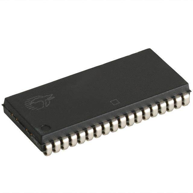
| 产品图片 |
|
| 产品型号 | M95020-RDW6TP |
| rohs | 无铅 / 符合限制有害物质指令(RoHS)规范要求 |
| 产品系列 | - |
| 产品目录页面 | |
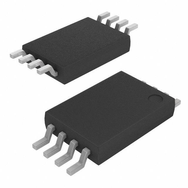
| 供应商器件封装 | 8-TSSOP |
| 其它名称 | 497-8673-1 |
| 其它有关文件 | http://www.st.com/web/catalog/mmc/FM76/CL1276/SC112/PF113584?referrer=70071840 |
| 包装 | 剪切带 (CT) |
| 存储器类型 | EEPROM |
| 存储容量 | 2K (256 x 8) |
| 封装/外壳 | 8-TSSOP(0.173",4.40mm 宽) |
| 工作温度 | -40°C ~ 85°C |
| 接口 | SPI 串行 |
| 标准包装 | 1 |
| 格式-存储器 | EEPROMs - 串行 |
| 电压-电源 | 1.8 V ~ 5.5 V |
| 速度 | 5MHz |


/IS61LPS102418B-200B3LI.jpg)


PDF Datasheet 数据手册内容提取
M950x0-W M950x0-R M950x0-DF 4 Kbit, 2 Kbit and 1 Kbit serial SPI bus EEPROM with high-speed clock Datasheet - production data Features • Compatible with SPI bus serial interface (Positive clock SPI modes) • Single supply voltage: – 2.5 V to 5.5 V for M950x0-W – 1.8 V to 5.5 V for M950x0-R – 1.7 V to 5.5 V for M95040-DF SO8 (MN) 150 mil width • High-speed 20 MHz clock rate, 5 ms write time • Memory array: – 1/2/4 Kbit (128/256/512 bytes) of EEPROM – Page size: 16 bytes – Write protection by block: 1/4, 1/2 or whole memory – Additional Write lockable Page (Identification page) TSSOP8 (DW) 169 mil width • Enhanced ESD protection • More than 4 million write cycles • More than 200-year data retention • Packages RoHS-compliant and Halogen-free (ECOPACK®) UFDFPN8 (MC) Table 1. Device summary 2 x 3 mm Reference Part number M95040-W M950x0-W M95020-W M95010-W M95040-R M950x0-R M95020-R M95010-R M950x0-DF M95040-DF August 2014 DocID6512 Rev 13 1/46 This is information on a product in full production. www.st.com
Contents M950x0-W M950x0-R M950x0-DF Contents 1 Description . . . . . . . . . . . . . . . . . . . . . . . . . . . . . . . . . . . . . . . . . . . . . . . . . 6 2 Signal description . . . . . . . . . . . . . . . . . . . . . . . . . . . . . . . . . . . . . . . . . . . 8 2.1 Serial Data Output (Q) . . . . . . . . . . . . . . . . . . . . . . . . . . . . . . . . . . . . . . . . 8 2.2 Serial Data Input (D) . . . . . . . . . . . . . . . . . . . . . . . . . . . . . . . . . . . . . . . . . . 8 2.3 Serial Clock (C) . . . . . . . . . . . . . . . . . . . . . . . . . . . . . . . . . . . . . . . . . . . . . 8 2.4 Chip Select (S) . . . . . . . . . . . . . . . . . . . . . . . . . . . . . . . . . . . . . . . . . . . . . . 8 2.5 Hold (HOLD) . . . . . . . . . . . . . . . . . . . . . . . . . . . . . . . . . . . . . . . . . . . . . . . . 8 2.6 Write Protect (W) . . . . . . . . . . . . . . . . . . . . . . . . . . . . . . . . . . . . . . . . . . . . 9 2.7 V ground . . . . . . . . . . . . . . . . . . . . . . . . . . . . . . . . . . . . . . . . . . . . . . . . . 9 SS 2.8 Supply voltage (V ) . . . . . . . . . . . . . . . . . . . . . . . . . . . . . . . . . . . . . . . . . 9 CC 2.8.1 Operating supply voltage (V ) . . . . . . . . . . . . . . . . . . . . . . . . . . . . . . . . 9 CC 2.8.2 Device reset . . . . . . . . . . . . . . . . . . . . . . . . . . . . . . . . . . . . . . . . . . . . . . . 9 2.8.3 Power-up conditions . . . . . . . . . . . . . . . . . . . . . . . . . . . . . . . . . . . . . . . 10 2.8.4 Power-down . . . . . . . . . . . . . . . . . . . . . . . . . . . . . . . . . . . . . . . . . . . . . . 10 3 Connecting to the SPI bus . . . . . . . . . . . . . . . . . . . . . . . . . . . . . . . . . . . 11 3.1 SPI modes . . . . . . . . . . . . . . . . . . . . . . . . . . . . . . . . . . . . . . . . . . . . . . . . 12 4 Operating features . . . . . . . . . . . . . . . . . . . . . . . . . . . . . . . . . . . . . . . . . 13 4.1 Hold condition . . . . . . . . . . . . . . . . . . . . . . . . . . . . . . . . . . . . . . . . . . . . . . 13 4.2 Status register . . . . . . . . . . . . . . . . . . . . . . . . . . . . . . . . . . . . . . . . . . . . . 13 4.3 Data protection and protocol control . . . . . . . . . . . . . . . . . . . . . . . . . . . . 14 5 Memory organization . . . . . . . . . . . . . . . . . . . . . . . . . . . . . . . . . . . . . . . 15 6 Instructions . . . . . . . . . . . . . . . . . . . . . . . . . . . . . . . . . . . . . . . . . . . . . . . 16 6.1 Write Enable (WREN) . . . . . . . . . . . . . . . . . . . . . . . . . . . . . . . . . . . . . . . 17 6.2 Write Disable (WRDI) . . . . . . . . . . . . . . . . . . . . . . . . . . . . . . . . . . . . . . . . 18 6.3 Read Status Register (RDSR) . . . . . . . . . . . . . . . . . . . . . . . . . . . . . . . . . 19 6.3.1 WIP bit . . . . . . . . . . . . . . . . . . . . . . . . . . . . . . . . . . . . . . . . . . . . . . . . . . 19 6.3.2 WEL bit . . . . . . . . . . . . . . . . . . . . . . . . . . . . . . . . . . . . . . . . . . . . . . . . . 19 6.3.3 BP1, BP0 bits . . . . . . . . . . . . . . . . . . . . . . . . . . . . . . . . . . . . . . . . . . . . . 20 2/46 DocID6512 Rev 13
M950x0-W M950x0-R M950x0-DF Contents 6.4 Write Status Register (WRSR) . . . . . . . . . . . . . . . . . . . . . . . . . . . . . . . . . 21 6.5 Read from Memory Array (READ) . . . . . . . . . . . . . . . . . . . . . . . . . . . . . . 22 6.6 Write to Memory Array (WRITE) . . . . . . . . . . . . . . . . . . . . . . . . . . . . . . . 23 6.7 Read Identification Page (available only in M95040-D device) . . . . . . . . 25 6.8 Write Identification Page (available only in M95040-D device) . . . . . . . . 26 6.9 Read Lock Status (available only in M95040-D device) . . . . . . . . . . . . . . 27 6.10 Lock Identification Page (available only in M95040-D device) . . . . . . . . . 28 7 Power-up and delivery states . . . . . . . . . . . . . . . . . . . . . . . . . . . . . . . . . 29 7.1 Power-up state . . . . . . . . . . . . . . . . . . . . . . . . . . . . . . . . . . . . . . . . . . . . . 29 7.2 Initial delivery state . . . . . . . . . . . . . . . . . . . . . . . . . . . . . . . . . . . . . . . . . . 29 8 Maximum rating . . . . . . . . . . . . . . . . . . . . . . . . . . . . . . . . . . . . . . . . . . . . 30 9 DC and AC parameters . . . . . . . . . . . . . . . . . . . . . . . . . . . . . . . . . . . . . . 31 10 Package mechanical data . . . . . . . . . . . . . . . . . . . . . . . . . . . . . . . . . . . . 40 11 Part numbering . . . . . . . . . . . . . . . . . . . . . . . . . . . . . . . . . . . . . . . . . . . . 43 12 Revision history . . . . . . . . . . . . . . . . . . . . . . . . . . . . . . . . . . . . . . . . . . . 44 DocID6512 Rev 13 3/46 3
List of tables M950x0-W M950x0-R M950x0-DF List of tables Table 1. Device summary. . . . . . . . . . . . . . . . . . . . . . . . . . . . . . . . . . . . . . . . . . . . . . . . . . . . . . . . . . 1 Table 2. Signal names . . . . . . . . . . . . . . . . . . . . . . . . . . . . . . . . . . . . . . . . . . . . . . . . . . . . . . . . . . . . 7 Table 3. Write-protected block size . . . . . . . . . . . . . . . . . . . . . . . . . . . . . . . . . . . . . . . . . . . . . . . . . 14 Table 4. Instruction set. . . . . . . . . . . . . . . . . . . . . . . . . . . . . . . . . . . . . . . . . . . . . . . . . . . . . . . . . . . 16 Table 5. Significant bits within the address byte. . . . . . . . . . . . . . . . . . . . . . . . . . . . . . . . . . . . . . . . 16 Table 6. Status register format. . . . . . . . . . . . . . . . . . . . . . . . . . . . . . . . . . . . . . . . . . . . . . . . . . . . . 19 Table 7. Address range bits . . . . . . . . . . . . . . . . . . . . . . . . . . . . . . . . . . . . . . . . . . . . . . . . . . . . . . . 22 Table 8. Absolute maximum ratings. . . . . . . . . . . . . . . . . . . . . . . . . . . . . . . . . . . . . . . . . . . . . . . . . 30 Table 9. Operating conditions (M950x0-W) . . . . . . . . . . . . . . . . . . . . . . . . . . . . . . . . . . . . . . . . . . . 31 Table 10. Operating conditions (M950x0-R). . . . . . . . . . . . . . . . . . . . . . . . . . . . . . . . . . . . . . . . . . . . 31 Table 11. Operating conditions (M95040-DF, device grade 6). . . . . . . . . . . . . . . . . . . . . . . . . . . . . . 31 Table 12. AC test measurement conditions . . . . . . . . . . . . . . . . . . . . . . . . . . . . . . . . . . . . . . . . . . . . 31 Table 13. Cycling performance. . . . . . . . . . . . . . . . . . . . . . . . . . . . . . . . . . . . . . . . . . . . . . . . . . . . . . 32 Table 14. Memory cell data retention. . . . . . . . . . . . . . . . . . . . . . . . . . . . . . . . . . . . . . . . . . . . . . . . . 32 Table 15. Capacitance . . . . . . . . . . . . . . . . . . . . . . . . . . . . . . . . . . . . . . . . . . . . . . . . . . . . . . . . . . . . 32 Table 16. DC characteristics (M950x0-W, device grade 6) . . . . . . . . . . . . . . . . . . . . . . . . . . . . . . . . 33 Table 17. DC characteristics (M950x0-R or M95040-DF, device grade 6). . . . . . . . . . . . . . . . . . . . . 34 Table 18. AC characteristics (M950x0-W, device grade 6). . . . . . . . . . . . . . . . . . . . . . . . . . . . . . . . . 35 Table 19. AC characteristics (M950x0-R or M95040-DF, device grade 6). . . . . . . . . . . . . . . . . . . . . 36 Table 20. AC characteristics (M950x0-W, device grade 6). . . . . . . . . . . . . . . . . . . . . . . . . . . . . . . . . 37 Table 21. AC characteristics (M950x0-R, device grade 6) . . . . . . . . . . . . . . . . . . . . . . . . . . . . . . . . 38 Table 22. SO8N 8-lead plastic small outline, 150 mils body width, package mechanical data . . . . . . . . . . . . . . . . . . . . . . . . . . . . . . . . . . . . . . . . . . . . . . . . . . . . . . . . . 40 Table 23. TSSOP8 8-lead thin shrink small outline, package mechanical data . . . . . . . . . . . . . . . . . 41 Table 24. UFDFPN8 (MLP8) 8-lead ultra thin fine pitch dual flat package no lead 2 × 3mm, data. . . . . . . . . . . . . . . . . . . . . . . . . . . . . . . . . . . . . . . . . . . . . . . . . . . . . . . . . . . 42 Table 25. Ordering information scheme. . . . . . . . . . . . . . . . . . . . . . . . . . . . . . . . . . . . . . . . . . . . . . . 43 Table 26. Document revision history . . . . . . . . . . . . . . . . . . . . . . . . . . . . . . . . . . . . . . . . . . . . . . . . . 44 4/46 DocID6512 Rev 13
M950x0-W M950x0-R M950x0-DF List of figures List of figures Figure 1. Logic diagram. . . . . . . . . . . . . . . . . . . . . . . . . . . . . . . . . . . . . . . . . . . . . . . . . . . . . . . . . . . . 6 Figure 2. 8-pin package connections. . . . . . . . . . . . . . . . . . . . . . . . . . . . . . . . . . . . . . . . . . . . . . . . . . 6 Figure 3. Bus master and memory devices on the SPI bus. . . . . . . . . . . . . . . . . . . . . . . . . . . . . . . . 11 Figure 4. SPI modes supported. . . . . . . . . . . . . . . . . . . . . . . . . . . . . . . . . . . . . . . . . . . . . . . . . . . . . 12 Figure 5. Hold condition activation. . . . . . . . . . . . . . . . . . . . . . . . . . . . . . . . . . . . . . . . . . . . . . . . . . . 13 Figure 6. Block diagram. . . . . . . . . . . . . . . . . . . . . . . . . . . . . . . . . . . . . . . . . . . . . . . . . . . . . . . . . . . 15 Figure 7. Write Enable (WREN) sequence . . . . . . . . . . . . . . . . . . . . . . . . . . . . . . . . . . . . . . . . . . . . 17 Figure 8. Write Disable (WRDI) sequence. . . . . . . . . . . . . . . . . . . . . . . . . . . . . . . . . . . . . . . . . . . . . 18 Figure 9. Read Status Register (RDSR) sequence. . . . . . . . . . . . . . . . . . . . . . . . . . . . . . . . . . . . . . 20 Figure 10. Write Status Register (WRSR) sequence. . . . . . . . . . . . . . . . . . . . . . . . . . . . . . . . . . . . . . 21 Figure 11. Read from Memory Array (READ) sequence . . . . . . . . . . . . . . . . . . . . . . . . . . . . . . . . . . . 22 Figure 12. Byte Write (WRITE) sequence . . . . . . . . . . . . . . . . . . . . . . . . . . . . . . . . . . . . . . . . . . . . . . 23 Figure 13. Page Write (WRITE) sequence . . . . . . . . . . . . . . . . . . . . . . . . . . . . . . . . . . . . . . . . . . . . . 24 Figure 14. Read Identification Page sequence . . . . . . . . . . . . . . . . . . . . . . . . . . . . . . . . . . . . . . . . . . 25 Figure 15. Write Identification Page sequence . . . . . . . . . . . . . . . . . . . . . . . . . . . . . . . . . . . . . . . . . . 26 Figure 16. Read Lock Status sequence. . . . . . . . . . . . . . . . . . . . . . . . . . . . . . . . . . . . . . . . . . . . . . . . 27 Figure 17. Lock ID sequence. . . . . . . . . . . . . . . . . . . . . . . . . . . . . . . . . . . . . . . . . . . . . . . . . . . . . . . . 28 Figure 18. AC test measurement I/O waveform(1) . . . . . . . . . . . . . . . . . . . . . . . . . . . . . . . . . . . . . . . 31 Figure 19. Serial input timing. . . . . . . . . . . . . . . . . . . . . . . . . . . . . . . . . . . . . . . . . . . . . . . . . . . . . . . . 39 Figure 20. Hold timing . . . . . . . . . . . . . . . . . . . . . . . . . . . . . . . . . . . . . . . . . . . . . . . . . . . . . . . . . . . . . 39 Figure 21. Serial output timing. . . . . . . . . . . . . . . . . . . . . . . . . . . . . . . . . . . . . . . . . . . . . . . . . . . . . . . 39 Figure 22. SO8N 8-lead plastic small outline 150 mils body width, package outline. . . . . . . . . . . . . . 40 Figure 23. TSSOP8 8-lead thin shrink small outline, package outline. . . . . . . . . . . . . . . . . . . . . . . . . 41 Figure 24. UFDFPN8 (MLP8) 8-lead ultra thin fine pitch dual flat package no lead 2 × 3mm, outline. . . . . . . . . . . . . . . . . . . . . . . . . . . . . . . . . . . . . . . . . . . . . . . . . . . . . . . . . 42 DocID6512 Rev 13 5/46 5
Description M950x0-W M950x0-R M950x0-DF 1 Description The M95010/ M95020/M95040 devices (M950x0) are electrically erasable programmable memories (EEPROMs) organized as 128/256/512 x 8 bits respectively, accessed through the SPI bus. The M950x0-W can operate with a supply voltage from 2.5 V to 5.5 V, the M950x0-R can operate with a supply voltage from 1.8 V to 5.5 V, and the M950x0-DF can operate with a supply voltage from 1.7 V to 5.5 V, over an ambient temperature range of -40 °C / +85 °C. The M950x0-DF offers an additional page, named the Identification Page (16 bytes). The Identification Page can be used to store sensitive application parameters which can be (later) permanently locked in Read-only mode. Figure 1. Logic diagram (cid:54)(cid:35)(cid:35) (cid:36) (cid:49) (cid:35) (cid:51) (cid:45)(cid:25)(cid:21)(cid:88)(cid:88)(cid:88) (cid:55) (cid:40)(cid:47)(cid:44)(cid:36) (cid:54)(cid:51)(cid:51) (cid:33)(cid:41)(cid:16)(cid:17)(cid:23)(cid:24)(cid:25)(cid:35) Figure 2. 8-pin package connections (cid:45)(cid:25)(cid:21)(cid:88)(cid:88)(cid:88) (cid:51) (cid:17) (cid:24) (cid:54)(cid:35)(cid:35) (cid:49) (cid:18) (cid:23) (cid:40)(cid:47)(cid:44)(cid:36) (cid:55) (cid:19) (cid:22) (cid:35) (cid:54)(cid:51)(cid:51) (cid:20) (cid:21) (cid:36) (cid:33)(cid:41)(cid:16)(cid:17)(cid:23)(cid:25)(cid:16)(cid:36) 1. See Section 10: Package mechanical data for package dimensions, and how to identify pin-1. 6/46 DocID6512 Rev 13
M950x0-W M950x0-R M950x0-DF Description Table 2. Signal names Signal name Function C Serial Clock D Serial Data input Q Serial Data output S Chip Select W Write Protect HOLD Hold V Supply voltage CC V Ground SS DocID6512 Rev 13 7/46 45
Signal description M950x0-W M950x0-R M950x0-DF 2 Signal description During all operations, V must be held stable and within the specified valid range: CC V (min) to V (max). CC CC All of the input and output signals can be held high or low (according to voltages of V , V , IH OH V or V , as specified in Table 16: DC characteristics (M950x0-W, device grade 6) and IL OL Table 17: DC characteristics (M950x0-R or M95040-DF, device grade 6). These signals are described next. 2.1 Serial Data Output (Q) This output signal transfers data serially out of the device. Data is shifted out on the falling edge of Serial Clock (C). 2.2 Serial Data Input (D) This input signal transfers data serially into the device. It receives instructions, addresses, and the data to be written. Values are latched on the rising edge of Serial Clock (C). 2.3 Serial Clock (C) This input signal provides the timing of the serial interface. Instructions, addresses, or data present at Serial Data Input (D) are latched on the rising edge of Serial Clock (C). Data on Serial Data Output (Q) changes after the falling edge of Serial Clock (C). 2.4 Chip Select (S) When this input signal is high, the device is deselected and Serial Data Output (Q) is at high impedance. Unless an internal Write cycle is in progress, the device will be in the Standby Power mode. Driving Chip Select (S) low selects the device, placing it in the Active Power mode. After Power-up, a falling edge on Chip Select (S) is required prior to the start of any instruction. 2.5 Hold (HOLD) The Hold (HOLD) signal is used to pause any serial communications with the device without deselecting the device. During the Hold condition, the Serial Data Output (Q) is high impedance, and Serial Data Input (D) and Serial Clock (C) are Don’t Care. To start the Hold condition, the device must be selected, with Chip Select (S) driven low. 8/46 DocID6512 Rev 13
M950x0-W M950x0-R M950x0-DF Signal description 2.6 Write Protect (W) This input signal controls whether the memory is write protected. When Write Protect (W) is held low, writes to the memory are disabled, but other operations remain enabled. Write Protect (W) must either be driven high or low, but must not be left floating. 2.7 V ground SS V is the reference for the V supply voltage. SS CC 2.8 Supply voltage (V ) CC 2.8.1 Operating supply voltage (V ) CC Prior to selecting the memory and issuing instructions to it, a valid and stable V voltage CC within the specified [V (min), V (max)] range must be applied (see Table 9: Operating CC CC conditions (M950x0-W), Table 10: Operating conditions (M950x0-R) and Table 11: Operating conditions (M95040-DF, device grade 6)). This voltage must remain stable and valid until the end of the transmission of the instruction and, for a Write instruction, until the completion of the internal write cycle (t ). W In order to secure a stable DC supply voltage, it is recommended to decouple the V line CC with a suitable capacitor (usually of the order of 10 nF to 100 nF) close to the V /V CC SS package pins. 2.8.2 Device reset In order to prevent inadvertent write operations during power-up, a power-on-reset (POR) circuit is included. At power-up, the device does not respond to any instruction until V CC reaches the internal reset threshold voltage (this threshold is defined in Table 9: Operating conditions (M950x0-W), Table 10: Operating conditions (M950x0-R) and Table 11: Operating conditions (M95040-DF, device grade 6) as V ). RES When V passes over the POR threshold, the device is reset and is in the following state: CC • Standby Power mode • Deselected (note that, to be executed, an instruction must be preceded by a falling edge on Chip Select (S)) • Status register value: – Write Enable Latch (WEL) is reset to 0 – Write In Progress (WIP) is reset to 0 – SRWD, BP1 and BP0 bits remain unchanged (non-volatile bits) When the device is in the above state, it must not be accessed until V reaches a valid and CC stable V voltage within the specified [V (min), V (max)] range defined in Table 9: CC CC CC Operating conditions (M950x0-W), Table 10: Operating conditions (M950x0-R) and Table 11: Operating conditions (M95040-DF, device grade 6). DocID6512 Rev 13 9/46 45
Signal description M950x0-W M950x0-R M950x0-DF 2.8.3 Power-up conditions When the power supply is turned on, V rises continuously from V to V . During this CC SS CC time, the Chip Select (S) line is not allowed to float but should follow the V voltage. It is CC therefore recommended to connect the S line to V via a suitable pull-up resistor (see CC Figure 3: Bus master and memory devices on the SPI bus). In addition, the Chip Select (S) input offers a built-in safety feature, as the S input is edge sensitive as well as level sensitive: after power-up, the device does not become selected until a falling edge has first been detected on Chip Select (S). This ensures that Chip Select (S) must have been high, prior to going low to start the first operation. The V voltage has to rise continuously from 0 V up to the minimum V operating voltage CC CC defined in Table 9: Operating conditions (M950x0-W), Table 10: Operating conditions (M950x0-R) and Table 11: Operating conditions (M95040-DF, device grade 6) and the rise time must not vary faster than 1 V/µs. 2.8.4 Power-down During power-down (continuous decrease in the V supply voltage below the minimum CC V operating voltage defined in Table 9: Operating conditions (M950x0-W), Table 10: CC Operating conditions (M950x0-R) and Table 11: Operating conditions (M95040-DF, device grade 6)), the device must be: • Deselected (Chip Select S should be allowed to follow the voltage applied on V ) CC • In Standby Power mode (there should not be any internal write cycle in progress). 10/46 DocID6512 Rev 13
M950x0-W M950x0-R M950x0-DF Connecting to the SPI bus 3 Connecting to the SPI bus The device is fully compatible with the SPI protocol. All instructions, addresses and input data bytes are shifted in to the device, most significant bit first. The Serial Data Input (D) is sampled on the first rising edge of the Serial Clock (C) after Chip Select (S) goes low. All output data bytes are shifted out of the device, most significant bit first. The Serial Data Output (Q) is latched on the first falling edge of the Serial Clock (C) after the instruction (such as the Read from Memory Array and Read Status Register instructions) have been clocked into the device. Figure 3: Bus master and memory devices on the SPI bus shows an example of three memory devices connected to an MCU, on an SPI bus. Only one memory device is selected at a time, so only one memory device drives the Serial Data output (Q) line at a time, the other memory devices are high impedance. The pull-up resistor R (represented in Figure 3: Bus master and memory devices on the SPI bus) ensures that a device is not selected if the bus master leaves the S line in the high impedance state. In applications where the bus master might enter a state where all SPI bus inputs/outputs would be in high impedance at the same time (for example, if the bus master is reset during the transmission of an Instruction), the clock line (C) must be connected to an external pull- down resistor so that, if all inputs/outputs become high impedance, the C line is pulled low (while the S line is pulled high): this ensures that S and C do not become high at the same time, and so, that the t requirement is met. The typical value of R is 100 kΩ.. SHCH Figure 3. Bus master and memory devices on the SPI bus V SS V CC R SDO SPI Interface with SDI (CPOL, CPHA) = (0, 0) or (1, 1) SCK C Q D V C Q D V C Q D V CC CC CC Bus master V V V SS SS SS R SPI mmory R SPI memory R SPI memory device device device CS3 CS2 CS1 S W HOLD S W HOLD S W HOLD AI12304b 1. The Write Protect (W) and Hold (HOLD) signals should be driven, high or low as appropriate. DocID6512 Rev 13 11/46 45
Connecting to the SPI bus M950x0-W M950x0-R M950x0-DF 3.1 SPI modes The device can be driven by a microcontroller with its SPI peripheral running in either of the following modes: • CPOL=0, CPHA=0 • CPOL=1, CPHA=1 For these two modes, input data is latched in on the rising edge of Serial Clock (C), and output data is available from the falling edge of Serial Clock (C). The difference between the two modes, as shown in Figure 4: SPI modes supported, is the clock polarity when the bus master is in Stand-by mode and not transferring data: • C remains at 0 for (CPOL=0, CPHA=0) • C remains at 1 for (CPOL=1, CPHA=1) Figure 4. SPI modes supported (cid:35)(cid:48)(cid:47)(cid:44)(cid:35)(cid:48)(cid:40)(cid:33) (cid:16) (cid:16) (cid:35) (cid:17) (cid:17) (cid:35) (cid:36) (cid:45)(cid:51)(cid:34) (cid:49) (cid:45)(cid:51)(cid:34) (cid:33)(cid:41)(cid:16)(cid:17)(cid:20)(cid:19)(cid:24)(cid:34) 12/46 DocID6512 Rev 13
M950x0-W M950x0-R M950x0-DF Operating features 4 Operating features 4.1 Hold condition The Hold (HOLD) signal is used to pause any serial communications with the device without resetting the clocking sequence. During the Hold condition, the Serial Data Output (Q) is high impedance, and Serial Data Input (D) and Serial Clock (C) are Don’t Care. To enter the Hold condition, the device must be selected, with Chip Select (S) low. Normally, the device is kept selected, for the whole duration of the Hold condition. Deselecting the device while it is in the Hold condition has the effect of resetting the state of the device, and this mechanism can be used if it is required to reset any processes that had been in progress. The Hold condition starts when the Hold (HOLD) signal is driven low at the same time as Serial Clock (C) already being low (as shown in Figure 5: Hold condition activation). The Hold condition ends when the Hold (HOLD) signal is driven high at the same time as Serial Clock (C) already being low. Figure 5: Hold condition activation also shows what happens if the rising and falling edges are not timed to coincide with Serial Clock (C) being low. Figure 5. Hold condition activation (cid:35) (cid:40)(cid:47)(cid:44)(cid:36) (cid:40)(cid:79)(cid:76)(cid:68) (cid:40)(cid:79)(cid:76)(cid:68) (cid:35)(cid:79)(cid:78)(cid:68)(cid:73)(cid:84)(cid:73)(cid:79)(cid:78) (cid:35)(cid:79)(cid:78)(cid:68)(cid:73)(cid:84)(cid:73)(cid:79)(cid:78) (cid:33)(cid:41)(cid:16)(cid:18)(cid:16)(cid:18)(cid:25)(cid:36) 4.2 Status register Figure 6 shows the position of the Status register in the control logic of the device. This register contains a number of control bits and status bits, as shown in Table 6: Status register format and as detailed in Section 6.3: Read Status Register (RDSR). DocID6512 Rev 13 13/46 45
Operating features M950x0-W M950x0-R M950x0-DF 4.3 Data protection and protocol control To help protect the device from data corruption in noisy or poorly controlled environments, a number of safety features have been built in to the device. The main security measures can be summarized as follows: • WEL bit is reset at power-up. • Chip Select (S) must rise after the eighth clock count (or multiple thereof) in order to start a non-volatile Write cycle (in the memory array or in the Status register). • Accesses to the memory array are ignored during the non-volatile programming cycle, and the programming cycle continues unaffected. • Invalid Chip Select (S) and Hold (HOLD) transitions are ignored. For any instruction to be accepted and executed, Chip Select (S) must be driven high after the rising edge of Serial Clock (C) that latches the last bit of the instruction, and before the next rising edge of Serial Clock (C). For this, “the last bit of the instruction” can be the eighth bit of the instruction code, or the eighth bit of a data byte, depending on the instruction (except in the case of RDSR and READ instructions). Moreover, the “next rising edge of CLOCK” might (or might not) be the next bus transaction for some other device on the bus. When a Write cycle is in progress, the device protects it against external interruption by ignoring any subsequent READ, WRITE or WRSR instruction until the present cycle is complete. Table 3. Write-protected block size Status register bits Protected array addresses Protected block BP1 BP0 M95040 M95020 M95010 0 0 none none none none 0 1 Upper quarter 180h - 1FFh C0h - FFh 60h - 7Fh 1 0 Upper half 100h - 1FFh 80h - FFh 40h - 7Fh 1 1 Whole memory 000h - 1FFh 00h - FFh 00h - 7Fh 14/46 DocID6512 Rev 13
M950x0-W M950x0-R M950x0-DF Memory organization 5 Memory organization The memory is organized as shown in Figure 6. Figure 6. Block diagram (cid:44)(cid:75)(cid:62)(cid:24) (cid:44)(cid:349)(cid:336)(cid:346)(cid:3)(cid:448)(cid:381)(cid:367)(cid:410)(cid:258)(cid:336)(cid:286) (cid:116) (cid:18)(cid:381)(cid:374)(cid:410)(cid:396)(cid:381)(cid:367)(cid:3)(cid:367)(cid:381)(cid:336)(cid:349)(cid:272) (cid:336)(cid:286)(cid:374)(cid:286)(cid:396)(cid:258)(cid:410)(cid:381)(cid:396) (cid:94) (cid:18) (cid:24) (cid:47)(cid:876)(cid:75)(cid:3)(cid:400)(cid:346)(cid:349)(cid:296)(cid:410)(cid:3)(cid:396)(cid:286)(cid:336)(cid:349)(cid:400)(cid:410)(cid:286)(cid:396) (cid:89) (cid:4)(cid:282)(cid:282)(cid:396)(cid:286)(cid:400)(cid:400)(cid:3)(cid:396)(cid:286)(cid:336)(cid:349)(cid:400)(cid:410)(cid:286)(cid:396) (cid:24)(cid:258)(cid:410)(cid:258) (cid:258)(cid:374)(cid:282)(cid:3)(cid:272)(cid:381)(cid:437)(cid:374)(cid:410)(cid:286)(cid:396) (cid:396)(cid:286)(cid:336)(cid:349)(cid:400)(cid:410)(cid:286)(cid:396) (cid:94)(cid:410)(cid:258)(cid:410)(cid:437)(cid:400) (cid:396)(cid:286)(cid:336)(cid:349)(cid:400)(cid:410)(cid:286)(cid:396) (cid:1005)(cid:876)(cid:1008) (cid:94)(cid:349)(cid:460)(cid:286)(cid:3)(cid:381)(cid:296)(cid:3)(cid:410)(cid:346)(cid:286) (cid:272)(cid:381)(cid:282)(cid:286)(cid:396) (cid:1005)(cid:876)(cid:1006) (cid:90)(cid:28)(cid:258)(cid:396)(cid:28)(cid:286)(cid:286)(cid:87)(cid:258)(cid:258)(cid:90)(cid:282)(cid:75)(cid:3)(cid:381)(cid:68)(cid:374)(cid:367)(cid:455) (cid:286) (cid:282) (cid:122)(cid:3) (cid:1005)(cid:3)(cid:393)(cid:258)(cid:336)(cid:286) (cid:47)(cid:282)(cid:286)(cid:374)(cid:410)(cid:349)(cid:296)(cid:349)(cid:272)(cid:258)(cid:410)(cid:349)(cid:381)(cid:374)(cid:3)(cid:393)(cid:258)(cid:336)(cid:286) (cid:121)(cid:3)(cid:282)(cid:286)(cid:272)(cid:381)(cid:282)(cid:286)(cid:396) (cid:48)(cid:54)(cid:20)(cid:28)(cid:26)(cid:22)(cid:22)(cid:57)(cid:20) DocID6512 Rev 13 15/46 45
Instructions M950x0-W M950x0-R M950x0-DF 6 Instructions Each command is composed of bytes (MSBit transmitted first), initiated with the instruction byte, as summarized in Table 4. If an invalid instruction is sent (one not contained in Table 4), the device automatically enters a Wait state until deselected. Table 4. Instruction set Instruction Instruction Description format WREN Write Enable 0000 X110(1) WRDI Write Disable 0000 X100(1) RDSR Read Status Register 0000 X101(1) WRSR Write Status Register 0000 X001(1) READ Read from Memory Array 0000 A 011(2) 8 WRITE Write to Memory Array 0000 A 010(2) 8 RDID(3) Read Identification Page 1000 0011 WRID(3) Write Identification Page 1000 0010 RDLS(3) Reads the Identification Page lock status. 1000 0011 LID(3) Locks the Identification page in read-only mode. 1000 0010 1. X = Don’t Care. 2. For M95040, A8 = 1 for the upper half of the memory array and 0 for the lower half, while for M95010 and M95020, A8 is Don’t Care. 3. Available only for the M95040-DF device. Table 5. Significant bits within the address byte(1)(2) Address byte Bit b3 of the Instructions instruction byte b7 b6 b5 b4 b3 b2 b1 b0 READ or WRITE A8/x(3) A7 A6 A5 A4 A3 A2 A1 A0 RDID or WRID 0 0 0 0 0 A3 A2 A1 A0 RDLS or LID 0 1 0 0 0 0 0 0 0 1. A: Significant address bit. 2. x: bit is Don’t Care. 3. For M95040, A8 = 1 for the upper half of the memory array and 0 for the lower half, while for M95010 and M95020, A8 is Don’t Care. 16/46 DocID6512 Rev 13
M950x0-W M950x0-R M950x0-DF Instructions 6.1 Write Enable (WREN) The Write Enable Latch (WEL) bit must be set prior to each WRITE and WRSR instruction. The only way to do this is to send a Write Enable instruction to the device. As shown in Figure 7: Write Enable (WREN) sequence, to send this instruction to the device, Chip Select (S) is driven low, and the bits of the instruction byte are shifted in, on Serial Data Input (D). The device then enters a wait state. It waits for a the device to be deselected, by Chip Select (S) being driven high. Figure 7. Write Enable (WREN) sequence (cid:54) (cid:19) (cid:20) (cid:21) (cid:22) (cid:23) (cid:24) (cid:25) (cid:26) (cid:38) (cid:44)(cid:81)(cid:86)(cid:87)(cid:85)(cid:88)(cid:70)(cid:87)(cid:76)(cid:82)(cid:81) (cid:39) (cid:43)(cid:76)(cid:74)(cid:75)(cid:3)(cid:44)(cid:80)(cid:83)(cid:72)(cid:71)(cid:68)(cid:81)(cid:70)(cid:72) (cid:52) (cid:36)(cid:44)(cid:19)(cid:20)(cid:23)(cid:23)(cid:20)(cid:39) DocID6512 Rev 13 17/46 45
Instructions M950x0-W M950x0-R M950x0-DF 6.2 Write Disable (WRDI) One way of resetting the Write Enable Latch (WEL) bit is to send a Write Disable instruction to the device. As shown in Figure 8: Write Disable (WRDI) sequence, to send this instruction to the device, Chip Select (S) is driven low, and the bits of the instruction byte are shifted in, on Serial Data Input (D). The device then enters a wait state. It waits for a the device to be deselected, by Chip Select (S) being driven high. The Write Enable Latch (WEL) bit is reset by any of the following events: • Power-up • WRDI instruction execution • WRSR instruction completion • WRITE instruction completion • Write Protect (W) line being held low. Figure 8. Write Disable (WRDI) sequence (cid:54) (cid:19) (cid:20) (cid:21) (cid:22) (cid:23) (cid:24) (cid:25) (cid:26) (cid:38) (cid:44)(cid:81)(cid:86)(cid:87)(cid:85)(cid:88)(cid:70)(cid:87)(cid:76)(cid:82)(cid:81) (cid:39) (cid:43)(cid:76)(cid:74)(cid:75)(cid:3)(cid:44)(cid:80)(cid:83)(cid:72)(cid:71)(cid:68)(cid:81)(cid:70)(cid:72) (cid:52) (cid:36)(cid:44)(cid:19)(cid:22)(cid:26)(cid:28)(cid:19)(cid:39) 18/46 DocID6512 Rev 13
M950x0-W M950x0-R M950x0-DF Instructions 6.3 Read Status Register (RDSR) The Read Status Register instruction is used to read the Status Register. As shown in Figure 9, to send this instruction to the device, Chip Select (S) is first driven low. The bits of the instruction byte are then shifted in, on Serial Data Input (D). The current state of the bits in the Status register is shifted out, on Serial Data Out (Q). The Read Cycle is terminated by driving Chip Select (S) high. The Status Register is always readable, even if a Write or Write Status Register cycle is in progress. During a Write Status Register cycle, the values of the non-volatile bits (BP0, BP1) become available when a new RDSR instruction is executed, after completion of the Write cycle. On the other hand, the two read-only bits (Write Enable Latch (WEL), Write In Progress (WIP)) are dynamically updated during the ongoing Write cycle. It is possible to read the Status Register contents continuously, as described in Figure 9. Bits b7, b6, b5 and b4 are always read as 1. The status and control bits of the Status register are as follows: Table 6. Status register format b7 b0 1 1 1 1 BP1 BP0 WEL WIP Block Protect bits Write Enable Latch bit Write In Progress bit 6.3.1 WIP bit The Write In Progress (WIP) bit indicates whether the memory is busy with a Write or Write Status register cycle. When set to 1, such a cycle is in progress, when reset to 0 no such cycle is in progress. 6.3.2 WEL bit The Write Enable Latch (WEL) bit indicates the status of the internal Write Enable Latch. When set to 1 the internal Write Enable Latch is set, when set to 0 the internal Write Enable Latch is reset and no Write or Write Status Register instruction is accepted. DocID6512 Rev 13 19/46 45
Instructions M950x0-W M950x0-R M950x0-DF 6.3.3 BP1, BP0 bits The Block Protect (BP1, BP0) bits are non-volatile. They define the size of the area to be software protected against Write instructions. These bits are written with the Write Status Register (WRSR) instruction. When one or both of the Block Protect (BP1, BP0) bits is set to 1, the relevant memory area (as defined in Table 3: Write-protected block size) becomes protected against Write (WRITE) instructions. The Block Protect (BP1, BP0) bits can be written provided that the Hardware Protected mode has not been set. Figure 9. Read Status Register (RDSR) sequence S 0 1 2 3 4 5 6 7 8 9 10 11 12 13 14 15 C Instruction D Status Register Out Status Register Out High Impedance Q 7 6 5 4 3 2 1 0 7 6 5 4 3 2 1 0 7 MSB MSB AI01444D 20/46 DocID6512 Rev 13
M950x0-W M950x0-R M950x0-DF Instructions 6.4 Write Status Register (WRSR) A Write Status Register (WRSR) instruction allows new values to be written to the Status register. Before it can be accepted, a Write Enable (WREN) instruction must previously have been executed. The WRSR instruction is entered by driving Chip Select (S) low, sending the instruction code followed by the data byte on Serial Data input (D), and driving the Chip Select (S) signal high. Chip Select (S) must be driven high after the rising edge of Serial Clock (C) that latches in the eighth bit of the data byte, and before the next rising edge of Serial Clock (C). Otherwise, the WRSR instruction is not executed. Driving the Chip Select (S) signal high at a byte boundary of the input data triggers the self- timed write cycle that takes t to complete (as specified in Table 16: DC characteristics W (M950x0-W, device grade 6) to Table 19: AC characteristics (M950x0-R or M95040-DF, device grade 6)). The instruction sequence is shown in Figure 10: Write Status Register (WRSR) sequence. While the Write Status Register cycle is in progress, the Status register may still be read to check the value of the Write in progress (WIP) bit: the WIP bit is 1 during the self-timed write cycle t , and, 0 when the write cycle is complete. The WEL bit (Write enable latch) is also W reset at the end of the write cycle t . W The WRSR instruction allows the user to change the values of the BP1, BP0 bits which define the size of the area that is to be treated as read only, as defined in Table 3: Write- protected block size. The contents of the BP1, BP0 bits are updated after the completion of the WRSR instruction, including the t write cycle. W The WRSR instruction has no effect on the b7, b6, b5, b4, b1 and b0 bits in the Status register which are always read as 0. Figure 10. Write Status Register (WRSR) sequence S 0 1 2 3 4 5 6 7 8 9 10 11 12 13 14 15 C Instruction Status Register In D 7 6 5 4 3 2 1 0 High Impedance MSB Q AI01445B The WRSR instruction is not accepted, and is not executed, under the following conditions: • if the Write Enable Latch (WEL) bit has not been set to 1 (by executing a Write Enable instruction just before) • if a write cycle is already in progress • if the device has not been deselected, by Chip Select (S) being driven high, after the eighth bit, b0, of the data byte has been latched in • if Write Protect (W) is low during the WRSR command (instruction, address and data) DocID6512 Rev 13 21/46 45
Instructions M950x0-W M950x0-R M950x0-DF 6.5 Read from Memory Array (READ) As shown in Figure 11: Read from Memory Array (READ) sequence, to send this instruction to the device, Chip Select (S) is first driven low. The bits of the instruction byte and address byte are then shifted in, on Serial Data Input (D). For the M95040, the most significant address bit, A8, is incorporated as bit b3 of the instruction byte, as shown in Table 4: Instruction set. The address is loaded into an internal address register, and the byte of data at that address is shifted out, on Serial Data Output (Q). If Chip Select (S) continues to be driven low, an internal bit-pointer is automatically incremented at each clock cycle, and the corresponding data bit is shifted out. When the highest address is reached, the address counter rolls over to zero, allowing the Read cycle to be continued indefinitely. The whole memory can, therefore, be read with a single READ instruction. The Read cycle is terminated by driving Chip Select (S) high. The rising edge of the Chip Select (S) signal can occur at any time during the cycle. The first byte addressed can be any byte within any page. The instruction is not accepted, and is not executed, if a Write cycle is currently in progress. Table 7. Address range bits Device M95040 M95020 M95010 Address Bits A8-A0 A7-A0 A6-A0 Figure 11. Read from Memory Array (READ) sequence (cid:51) (cid:16) (cid:17) (cid:18) (cid:19) (cid:20) (cid:21) (cid:22) (cid:23) (cid:24) (cid:25) (cid:17)(cid:16) (cid:17)(cid:17) (cid:17)(cid:18) (cid:17)(cid:19) (cid:17)(cid:20) (cid:17)(cid:21) (cid:17)(cid:22) (cid:17)(cid:23) (cid:17)(cid:24) (cid:17)(cid:25) (cid:18)(cid:16) (cid:18)(cid:17) (cid:18)(cid:18) (cid:35) (cid:41)(cid:78)(cid:83)(cid:84)(cid:82)(cid:85)(cid:67)(cid:84)(cid:73)(cid:79)(cid:78) (cid:34)(cid:89)(cid:84)(cid:69)(cid:0)(cid:33)(cid:68)(cid:68)(cid:82)(cid:69)(cid:83)(cid:83) (cid:36) (cid:33)(cid:24) (cid:33)(cid:23) (cid:33)(cid:22) (cid:33)(cid:21) (cid:33)(cid:20) (cid:33)(cid:19) (cid:33)(cid:18) (cid:33)(cid:17) (cid:33)(cid:16) (cid:36)(cid:65)(cid:84)(cid:65)(cid:0)(cid:47)(cid:85)(cid:84) (cid:40)(cid:73)(cid:71)(cid:72)(cid:0)(cid:41)(cid:77)(cid:80)(cid:69)(cid:68)(cid:65)(cid:78)(cid:67)(cid:69) (cid:49) (cid:23) (cid:22) (cid:21) (cid:20) (cid:19) (cid:18) (cid:17) (cid:16) (cid:33)(cid:41)(cid:16)(cid:17)(cid:20)(cid:20)(cid:16)(cid:37) 1. Depending on the memory size, as shown in Table 7: Address range bits, the most significant address bits are Don’t Care. 22/46 DocID6512 Rev 13
M950x0-W M950x0-R M950x0-DF Instructions 6.6 Write to Memory Array (WRITE) As shown in Figure 12: Byte Write (WRITE) sequence, to send this instruction to the device, Chip Select (S) is first driven low. The bits of the instruction byte, address byte, and at least one data byte are then shifted in, on Serial Data input (D). The instruction is terminated by driving Chip Select (S) high at a byte boundary of the input data. The self-timed Write cycle, triggered by the rising edge of Chip Select (S), continues for a period t (as specified in W Table 16: DC characteristics (M950x0-W, device grade 6) to Table 19: AC characteristics (M950x0-R or M95040-DF, device grade 6)). After this time, the Write in Progress (WIP) bit is reset to 0. In the case of Figure 12: Byte Write (WRITE) sequence, Chip Select (S) is driven high after the eighth bit of the data byte has been latched in, indicating that the instruction is being used to write a single byte. If, though, Chip Select (S) continues to be driven low, as shown in Figure 13: Page Write (WRITE) sequence, the next byte of input data is shifted in, so that more than a single byte, starting from the given address towards the end of the same page, can be written in a single internal Write cycle. If Chip Select (S) still continues to be driven low, the next byte of input data is shifted in, and used to overwrite the byte at the start of the current page. The instruction is not accepted, and is not executed, under the following conditions: • if the Write Enable Latch (WEL) bit has not been set to 1 (by executing a Write Enable instruction just before) • if a Write cycle is already in progress • if the device has not been deselected, by Chip Select (S) being driven high, at a byte boundary (after the rising edge of Serial Clock (C) that latches the last data bit, and before the next rising edge of Serial Clock (C) occurs anywhere on the bus) • if Write Protect (W) is low or if the addressed page is in the area protected by the Block Protect (BP1 and BP0) bits Note: The self-timed write cycle t is internally executed as a sequence of two consecutive W events: [Erase addressed byte(s)], followed by [Program addressed byte(s)]. An erased bit is read as “0” and a programmed bit is read as “1”. Figure 12. Byte Write (WRITE) sequence (cid:94) (cid:1004) (cid:1005) (cid:1006) (cid:1007) (cid:1008) (cid:1009) (cid:1010) (cid:1011) (cid:1012) (cid:1013) (cid:1005)(cid:1004) (cid:1005)(cid:1005) (cid:1005)(cid:1006) (cid:1005)(cid:1007) (cid:1005)(cid:1008) (cid:1005)(cid:1009) (cid:1005)(cid:1010) (cid:1005)(cid:1011) (cid:1005)(cid:1012) (cid:1005)(cid:1013) (cid:1006)(cid:1004) (cid:1006)(cid:1005) (cid:1006)(cid:1006) (cid:1006)(cid:1007) (cid:18) (cid:47)(cid:374)(cid:400)(cid:410)(cid:396)(cid:437)(cid:272)(cid:410)(cid:349)(cid:381)(cid:374) (cid:17)(cid:455)(cid:410)(cid:286)(cid:3)(cid:4)(cid:282)(cid:282)(cid:396)(cid:286)(cid:400)(cid:400) (cid:24)(cid:258)(cid:410)(cid:258)(cid:3)(cid:17)(cid:455)(cid:410)(cid:286) (cid:24) (cid:4)(cid:1012) (cid:4)(cid:1011) (cid:4)(cid:1010) (cid:4)(cid:1009) (cid:4)(cid:1008) (cid:4)(cid:1007) (cid:4)(cid:1006) (cid:4)(cid:1005) (cid:4)(cid:1004) (cid:1011) (cid:1010) (cid:1009) (cid:1008) (cid:1007) (cid:1006) (cid:1005) (cid:1004) (cid:44)(cid:349)(cid:336)(cid:346)(cid:3)(cid:47)(cid:373)(cid:393)(cid:286)(cid:282)(cid:258)(cid:374)(cid:272)(cid:286) (cid:89) (cid:36)(cid:44)(cid:19)(cid:20)(cid:23)(cid:23)(cid:21)(cid:39) 1. Depending on the memory size, as shown in Table 7: Address range bits, the most significant address bits are Don’t Care. DocID6512 Rev 13 23/46 45
Instructions M950x0-W M950x0-R M950x0-DF Figure 13. Page Write (WRITE) sequence (cid:51) (cid:16) (cid:17) (cid:18) (cid:19) (cid:20) (cid:21) (cid:22) (cid:23) (cid:24) (cid:25) (cid:17)(cid:16) (cid:17)(cid:17) (cid:17)(cid:18) (cid:17)(cid:19) (cid:17)(cid:20) (cid:17)(cid:21) (cid:17)(cid:22) (cid:17)(cid:23) (cid:17)(cid:24) (cid:17)(cid:25) (cid:18)(cid:16) (cid:18)(cid:17) (cid:18)(cid:18) (cid:18)(cid:19) (cid:35) (cid:41)(cid:78)(cid:83)(cid:84)(cid:82)(cid:85)(cid:67)(cid:84)(cid:73)(cid:79)(cid:78) (cid:34)(cid:89)(cid:84)(cid:69)(cid:0)(cid:33)(cid:68)(cid:68)(cid:82)(cid:69)(cid:83)(cid:83) (cid:36)(cid:65)(cid:84)(cid:65)(cid:0)(cid:34)(cid:89)(cid:84)(cid:69)(cid:0)(cid:17) (cid:36) (cid:33)(cid:24) (cid:33)(cid:23) (cid:33)(cid:22) (cid:33)(cid:21) (cid:33)(cid:20) (cid:33)(cid:19) (cid:33)(cid:18) (cid:33)(cid:17) (cid:33)(cid:16) (cid:23) (cid:22) (cid:21) (cid:20) (cid:19) (cid:18) (cid:17) (cid:16) (cid:23) (cid:51) (cid:46) (cid:46) (cid:46) (cid:46) (cid:46) (cid:46) (cid:46) (cid:46) (cid:24) (cid:24) (cid:24) (cid:24) (cid:24) (cid:24) (cid:24) (cid:24) (cid:11) (cid:11) (cid:11) (cid:11) (cid:11) (cid:11) (cid:22) (cid:23) (cid:24) (cid:25) (cid:16) (cid:17) (cid:18) (cid:19) (cid:11) (cid:11) (cid:16) (cid:17) (cid:18) (cid:19) (cid:20) (cid:21) (cid:19) (cid:19) (cid:19) (cid:19) (cid:20) (cid:20) (cid:20) (cid:20) (cid:18)(cid:20) (cid:18)(cid:21) (cid:18)(cid:22) (cid:18)(cid:23) (cid:18)(cid:24) (cid:18)(cid:25) (cid:19)(cid:16) (cid:19)(cid:17) (cid:24) (cid:25) (cid:17) (cid:17) (cid:17) (cid:17) (cid:17) (cid:17) (cid:17) (cid:17) (cid:17) (cid:17) (cid:17) (cid:17) (cid:17) (cid:17) (cid:35) (cid:36)(cid:65)(cid:84)(cid:65)(cid:0)(cid:34)(cid:89)(cid:84)(cid:69)(cid:0)(cid:18) (cid:36)(cid:65)(cid:84)(cid:65)(cid:0)(cid:34)(cid:89)(cid:84)(cid:69)(cid:0)(cid:46) (cid:36)(cid:65)(cid:84)(cid:65)(cid:0)(cid:34)(cid:89)(cid:84)(cid:69)(cid:0)(cid:17)(cid:22) (cid:36) (cid:23) (cid:22) (cid:21) (cid:20) (cid:19) (cid:18) (cid:17) (cid:16) (cid:23) (cid:22) (cid:21) (cid:20) (cid:19) (cid:18) (cid:17) (cid:16) (cid:23) (cid:22) (cid:21) (cid:20) (cid:19) (cid:18) (cid:17) (cid:16) (cid:33)(cid:41)(cid:16)(cid:17)(cid:20)(cid:20)(cid:19)(cid:36) 1. Depending on the memory size, as shown in Table 7: Address range bits, the most significant address bits are Don’t Care. 24/46 DocID6512 Rev 13
M950x0-W M950x0-R M950x0-DF Instructions 6.7 Read Identification Page (available only in M95040-D device) The Read Identification Page (RDID) instruction is used to read the Identification Page (additional page of 16 bytes which can be written and later permanently locked in Read-only mode). The Chip Select (S) signal is first driven low, the bits of the instruction byte and address bytes are then shifted in (MSB first) on Serial Data input (D). Address bit A7 must be 0 and the other address bits are Don't Care except the lower address bits [A3:A0] (it might be easier to define these bits as 0, as shown in Table 5). Data is then shifted/clocked out (MSB first) on Serial Data output (Q). The first byte addressed can be any byte within the identification page. If Chip Select (S) continues to be driven low, the internal address register is automatically incremented and the byte of data at the new address is shifted out. Note that there is no roll over feature in the Identification Page. The address of bytes to read must not exceed the page boundary. The read cycle is terminated by driving Chip Select (S) high. The rising edge of the Chip Select (S) signal can occur at any time when the data bits are shifted out. The instruction is not accepted, and is not executed, if a Write cycle is currently in progress. Figure 14. Read Identification Page sequence (cid:51) (cid:16) (cid:17) (cid:18) (cid:19) (cid:20) (cid:21) (cid:22) (cid:23) (cid:24) (cid:25) (cid:17)(cid:16) (cid:17)(cid:17) (cid:17)(cid:18) (cid:17)(cid:19) (cid:17)(cid:20) (cid:17)(cid:21) (cid:17)(cid:22) (cid:17)(cid:23) (cid:17)(cid:24) (cid:17)(cid:25) (cid:18)(cid:16) (cid:18)(cid:17) (cid:18)(cid:18) (cid:35) (cid:41)(cid:78)(cid:83)(cid:84)(cid:82)(cid:85)(cid:67)(cid:84)(cid:73)(cid:79)(cid:78) (cid:34)(cid:89)(cid:84)(cid:69)(cid:0)(cid:33)(cid:68)(cid:68)(cid:82)(cid:69)(cid:83)(cid:83) (cid:36) (cid:33)(cid:23) (cid:33)(cid:22) (cid:33)(cid:21) (cid:33)(cid:20) (cid:33)(cid:19) (cid:33)(cid:18) (cid:33)(cid:17) (cid:33)(cid:16) (cid:36)(cid:65)(cid:84)(cid:65)(cid:0)(cid:47)(cid:85)(cid:84) (cid:40)(cid:73)(cid:71)(cid:72)(cid:0)(cid:41)(cid:77)(cid:80)(cid:69)(cid:68)(cid:65)(cid:78)(cid:67)(cid:69) (cid:49) (cid:23) (cid:22) (cid:21) (cid:20) (cid:19) (cid:18) (cid:17) (cid:16) (cid:45)(cid:51)(cid:19)(cid:17)(cid:22)(cid:19)(cid:16)(cid:54)(cid:17) DocID6512 Rev 13 25/46 45
Instructions M950x0-W M950x0-R M950x0-DF 6.8 Write Identification Page (available only in M95040-D device) The Write Identification Page (WRID) instruction is used to write the Identification Page (additional page of 16 bytes which can also be permanently locked in Read-only mode). The Chip Select signal (S) is first driven low, and then the bits of the instruction byte, address bytes, and at least one data byte are shifted in (MSB first) on Serial Data input (D). Address bit A7 must be 0 and the other address bits are Don't Care except the lower address bits [A3:A0] (it might be easier to define these bits as 0, as shown in Table 5). The self-timed Write cycle starts from the rising edge of Chip Select (S), and continues for a period t (as specified in Chapter 9: DC and AC parameters). W Figure 15. Write Identification Page sequence (cid:94) (cid:1004) (cid:1005) (cid:1006) (cid:1007) (cid:1008) (cid:1009) (cid:1010) (cid:1011) (cid:1012) (cid:1013) (cid:1005)(cid:1004) (cid:1005)(cid:1005) (cid:1005)(cid:1006) (cid:1005)(cid:1007) (cid:1005)(cid:1008) (cid:1005)(cid:1009) (cid:1005)(cid:1010) (cid:1005)(cid:1011) (cid:1005)(cid:1012) (cid:1005)(cid:1013) (cid:1006)(cid:1004) (cid:1006)(cid:1005) (cid:1006)(cid:1006) (cid:1006)(cid:1007) (cid:18) (cid:47)(cid:374)(cid:400)(cid:410)(cid:396)(cid:437)(cid:272)(cid:410)(cid:349)(cid:381)(cid:374) (cid:17)(cid:455)(cid:410)(cid:286)(cid:3)(cid:4)(cid:282)(cid:282)(cid:396)(cid:286)(cid:400)(cid:400) (cid:24)(cid:258)(cid:410)(cid:258)(cid:3)(cid:17)(cid:455)(cid:410)(cid:286) (cid:24) (cid:4)(cid:1011) (cid:4)(cid:1010) (cid:4)(cid:1009) (cid:4)(cid:1008) (cid:4)(cid:1007) (cid:4)(cid:1006) (cid:4)(cid:1005) (cid:4)(cid:1004) (cid:1011) (cid:1010) (cid:1009) (cid:1008) (cid:1007) (cid:1006) (cid:1005) (cid:1004) (cid:44)(cid:349)(cid:336)(cid:346)(cid:3)(cid:47)(cid:373)(cid:393)(cid:286)(cid:282)(cid:258)(cid:374)(cid:272)(cid:286) (cid:89) (cid:48)(cid:54)(cid:22)(cid:20)(cid:25)(cid:22)(cid:20)(cid:57)(cid:20) The instruction is discarded, and is not executed if the Block Protect bits (BP1,BP0) = (1,1) or one of the conditions defined in Section 4.3: Data protection and protocol control is not satisfied. 26/46 DocID6512 Rev 13
M950x0-W M950x0-R M950x0-DF Instructions 6.9 Read Lock Status (available only in M95040-D device) The Read Lock Status (RDLS) instruction is used to read the lock status. To send this instruction to the device, Chip Select (S) first has to be driven low. The bits of the instruction byte and address bytes are then shifted in (MSB first) on Serial Data input (D). Address bit A7 must be 1; all other address bits are Don't Care (it might be easier to define these bits as 0, as shown in Table 5). The Lock bit is the LSB (Least Significant Bit) of the byte read on Serial Data output (Q). It is at ‘1’ when the lock is active and at ‘0’ when the lock is not active. If Chip Select (S) continues to be driven low, the same data byte is shifted out. The read cycle is terminated by driving Chip Select (S) high. The instruction sequence is shown in Figure 16. The Read Lock Status instruction is not accepted and not executed if a Write cycle is currently in progress. Figure 16. Read Lock Status sequence (cid:51) (cid:16) (cid:17) (cid:18) (cid:19) (cid:20) (cid:21) (cid:22) (cid:23) (cid:24) (cid:25) (cid:17)(cid:16) (cid:17)(cid:17) (cid:17)(cid:18) (cid:17)(cid:19) (cid:17)(cid:20) (cid:17)(cid:21) (cid:17)(cid:22) (cid:17)(cid:23) (cid:17)(cid:24) (cid:17)(cid:25) (cid:18)(cid:16) (cid:18)(cid:17) (cid:18)(cid:18) (cid:35) (cid:41)(cid:78)(cid:83)(cid:84)(cid:82)(cid:85)(cid:67)(cid:84)(cid:73)(cid:79)(cid:78) (cid:34)(cid:89)(cid:84)(cid:69)(cid:0)(cid:33)(cid:68)(cid:68)(cid:82)(cid:69)(cid:83)(cid:83) (cid:36) (cid:33)(cid:23) (cid:33)(cid:22) (cid:33)(cid:21) (cid:33)(cid:20) (cid:33)(cid:19) (cid:33)(cid:18) (cid:33)(cid:17) (cid:33)(cid:16) (cid:36)(cid:65)(cid:84)(cid:65)(cid:0)(cid:47)(cid:85)(cid:84) (cid:40)(cid:73)(cid:71)(cid:72)(cid:0)(cid:41)(cid:77)(cid:80)(cid:69)(cid:68)(cid:65)(cid:78)(cid:67)(cid:69) (cid:49) (cid:23) (cid:22) (cid:21) (cid:20) (cid:19) (cid:18) (cid:17) (cid:16) (cid:45)(cid:51)(cid:19)(cid:17)(cid:22)(cid:19)(cid:16)(cid:54)(cid:17) DocID6512 Rev 13 27/46 45
Instructions M950x0-W M950x0-R M950x0-DF 6.10 Lock Identification Page (available only in M95040-D device) The Lock Identification Page (LID) command is used to permanently lock the Identification Page in Read-only mode. The LID instruction is issued by driving Chip Select (S) low, sending (MSB first) the instruction code, the address and a data byte on Serial Data input (D), and driving Chip Select (S) high. In the address sent, A7 must be equal to 1. All other address bits are Don't Care (it might be easier to define these bits as 0, as shown in Table 5). The data byte sent must be equal to the binary value xxxx xx1x, where x = Don't Care. The LID instruction is terminated by driving Chip Select (S) high at a data byte boundary, otherwise, the instruction is not executed. Figure 17. Lock ID sequence (cid:94) (cid:1004) (cid:1005) (cid:1006) (cid:1007) (cid:1008) (cid:1009) (cid:1010) (cid:1011) (cid:1012) (cid:1013) (cid:1005)(cid:1004) (cid:1005)(cid:1007) (cid:1005)(cid:1008) (cid:1005)(cid:1009) (cid:1005)(cid:1010) (cid:1005)(cid:1011) (cid:1005)(cid:1012) (cid:1005)(cid:1013) (cid:1006)(cid:1004) (cid:1006)(cid:1005) (cid:1006)(cid:1006) (cid:1006)(cid:1007) (cid:1006)(cid:1008) (cid:1006)(cid:1009) (cid:18) (cid:47)(cid:374)(cid:400)(cid:410)(cid:396)(cid:437)(cid:272)(cid:410)(cid:349)(cid:381)(cid:374) (cid:1012)(cid:882)(cid:271)(cid:349)(cid:410)(cid:3)(cid:258)(cid:282)(cid:282)(cid:396)(cid:286)(cid:400)(cid:400) (cid:24)(cid:258)(cid:410)(cid:258)(cid:3)(cid:271)(cid:455)(cid:410)(cid:286) (cid:24) (cid:1011) (cid:1010) (cid:1009) (cid:1007) (cid:1006) (cid:1005) (cid:1004) (cid:1011) (cid:1010) (cid:1009) (cid:1008) (cid:1007) (cid:1006) (cid:1005) (cid:1004) (cid:44)(cid:349)(cid:336)(cid:346)(cid:3)(cid:349)(cid:373)(cid:393)(cid:286)(cid:282)(cid:258)(cid:374)(cid:272)(cid:286) (cid:89) (cid:68)(cid:94)(cid:1007)(cid:1005)(cid:1010)(cid:1007)(cid:1006)(cid:115)(cid:1005) Driving Chip Select (S) high at a byte boundary of the input data triggers the self-timed Write cycle which duration is t (specified in Section 9: DC and AC parameters). The instruction W sequence is shown in Figure 17. The instruction is discarded, and is not executed if the Block Protect bits (BP1,BP0) = (1,1) or one of the conditions defined in Section 4.3: Data protection and protocol control is not satisfied. 28/46 DocID6512 Rev 13
M950x0-W M950x0-R M950x0-DF Power-up and delivery states 7 Power-up and delivery states 7.1 Power-up state After Power-up, the device is in the following state: • Low power Standby Power mode • Deselected (after Power-up, a falling edge is required on Chip Select (S) before any instructions can be started) • Not in Hold Condition • Write Enable Latch (WEL) is reset to 0 • Write In Progress (WIP) is reset to 0 The BP1 and BP0 bits of the Status register are unchanged from the previous power-down (they are non-volatile bits). 7.2 Initial delivery state The device is delivered with: • the memory array set to all 1s (each byte = FFh) • Status register: bit SRWD =0, BP1 =0 and BP0 =0 • M95040-D only: the identification page bytes values are Don’t Care. DocID6512 Rev 13 29/46 45
Maximum rating M950x0-W M950x0-R M950x0-DF 8 Maximum rating Stressing the device outside the ratings listed in Table 8: Absolute maximum ratings may cause permanent damage to the device. These are stress ratings only, and operation of the device at these, or any other conditions outside those indicated in the operating sections of this specification, is not implied. Exposure to absolute maximum rating conditions for extended periods may affect device reliability. Table 8. Absolute maximum ratings Symbol Parameter Min. Max. Unit T Ambient operating temperature –40 130 °C AMR T Storage temperature –65 150 °C STG T Lead temperature during soldering see note (1) °C LEAD V Output voltage –0.50 V +0.6 V O CC V Input voltage –0.50 V +1.0 V I CC I DC output current (Q = 0) - 5 mA OL I DC output current (Q = 1) - 5 mA IH V Supply voltage –0.50 6.5 V CC V Electrostatic pulse (Human Body Model) voltage(2) - 4000 V ESD 1. Compliant with JEDEC standard J-STD-020D (for small-body, Sn-Pb or Pb assembly), the ST ECOPACK® 7191395 specification, and the European directive on Restrictions on Hazardous Substances (RoHS directive 2011/65/EU of July 2011). 2. Positive and negative pulses applied on pin pairs, according to the AEC-Q100-002 (compliant with JEDEC Std JESD22-A114, C1=100pF, R1=1500 Ω, R2=500 Ω). 30/46 DocID6512 Rev 13
M950x0-W M950x0-R M950x0-DF DC and AC parameters 9 DC and AC parameters This section summarizes the operating and measurement conditions, and the DC and AC characteristics of the device. Table 9. Operating conditions (M950x0-W) Symbol Parameter Min. Max. Unit V Supply voltage 2.5 5.5 V CC T Ambient operating temperature (device grade 6) –40 85 °C A Table 10. Operating conditions (M950x0-R) Symbol Parameter Min. Max. Unit V Supply voltage 1.8 5.5 V CC T Ambient operating temperature –40 85 °C A Table 11. Operating conditions (M95040-DF, device grade 6) Symbol Parameter Min. Max. Unit V Supply voltage 1.7 5.5 V CC T Ambient operating temperature –40 85 °C A Table 12. AC test measurement conditions Symbol Parameter Min. Max. Unit C Load capacitance 30 pF L - Input rise and fall times - 50 ns - Input pulse voltages 0.2V to 0.8V V CC CC - Input and output timing reference voltages 0.3V to 0.7V V CC CC Figure 18. AC test measurement I/O waveform(1) (cid:44)(cid:81)(cid:83)(cid:88)(cid:87)(cid:3)(cid:47)(cid:72)(cid:89)(cid:72)(cid:79)(cid:86) (cid:44)(cid:81)(cid:83)(cid:88)(cid:87)(cid:3)(cid:68)(cid:81)(cid:71)(cid:3)(cid:50)(cid:88)(cid:87)(cid:83)(cid:88)(cid:87)(cid:3)(cid:55)(cid:76)(cid:80)(cid:76)(cid:81)(cid:74)(cid:3) (cid:53)(cid:72)(cid:73)(cid:72)(cid:85)(cid:72)(cid:81)(cid:70)(cid:72)(cid:3)(cid:47)(cid:72)(cid:89)(cid:72)(cid:79)(cid:86) (cid:19)(cid:17)(cid:27)(cid:57) (cid:38)(cid:38) (cid:19)(cid:17)(cid:26)(cid:57) (cid:38)(cid:38) (cid:19)(cid:17)(cid:22)(cid:57) (cid:38)(cid:38) (cid:19)(cid:17)(cid:21)(cid:57) (cid:38)(cid:38) (cid:68)(cid:76)(cid:19)(cid:19)(cid:27)(cid:21)(cid:24)(cid:71) 1. Output Hi-Z is defined as the point where data out is no longer driven. DocID6512 Rev 13 31/46 45
DC and AC parameters M950x0-W M950x0-R M950x0-DF Table 13. Cycling performance(1) Symbol Parameter Test conditions Min. Max. Unit T ≤ 25 °C, A - 4,000,000 V (min) < V < V (max) CC CC CC Ncycle Write cycle endurance Write cycle T = 85 °C, A - 1,200,000 V (min) < V < V (max) CC CC CC 1. Cycling performance for products identified by process letter K (previous products were specified with 1 million cycles at 25 °C). Table 14. Memory cell data retention(1) Parameter Test conditions Min. Unit Data retention T = 55 °C 200 Year A 1. For products identified by process letter K (previous products were specified with a data retention of 40 years at 55°C). The data retention behavior is checked in production, while the 200-year limit is defined from characterization and qualification results. Table 15. Capacitance (1) Symbol Parameter Test condition Min. Max. Unit C Output capacitance (Q) V = 0 V - 8 pF OUT OUT Input capacitance (D) V = 0 V - 8 pF IN C IN Input capacitance (other pins) V = 0 V - 6 pF IN 1. Sampled only, not 100% tested, at TA=25 °C and a frequency of 5 MHz. 32/46 DocID6512 Rev 13
M950x0-W M950x0-R M950x0-DF DC and AC parameters Table 16. DC characteristics (M950x0-W, device grade 6) Test conditions in addition to those Symbol Parameter Min. Max. Unit defined in Table 9 Input leakage I V = V orV - ± 2 µA LI current IN SS CC Output leakage I S = V , V = V orV - ± 2 µA LO current CC OUT SS CC V = 2.5 V, f = 5 MHz, CC C - 2 C = 0.1 V /0.9 V Q = open CC CC, I Supply current VCC = 2.5 V, fC = 10 MHz, - 2 mA CC (Read) C = 0.1 V /0.9 V Q = open CC CC, V = 5.5 V, f = 20 MHz, CC C - 5 (1) C = 0.1 V /0.9 V Q = open CC CC, Supply current I (2) During t , S = V , 2.5 V < V < 5.5 V - 5 mA CC0 (Write) W CC CC S = V , V = 5.5 V, CC CC - 3(3) Supply current VIN = VSS or VCC, I µA CC1 (Standby) S = V , V = 2.5 V, CC CC - 2 (4) V = V orV , IN SS CC V Input low voltage - –0.45 0.3 V V IL CC V Input high voltage - 0.7 V V +1 V IH CC CC V Output low voltage I = 1.5 mA, V = 2.5 V - 0.4 V OL OL CC V = 2.5 V and I = 0.4 mA or V Output high voltage CC OH 0.8 V - V OH V = 5 V and I = 2 mA CC CC OH Internal reset V (2) - 1.0(5) 1.65(6) V RES threshold voltage 1. Only for the devices identified by process letter K. 2. Characterized only, not tested in production. 3. 2 µA for the devices identified by process letter G or S. 4. 1 µA for the devices identified by process letter G or S. 5. 0.5 V with the device identified by process letter K. 6. 1.5 V with the device identified by process letter K. DocID6512 Rev 13 33/46 45
DC and AC parameters M950x0-W M950x0-R M950x0-DF Table 17. DC characteristics (M950x0-R or M95040-DF, device grade 6) Test conditions in addition to those defined Symbol Parameter Min. Max. Unit in Table 10 or Table 11 and Table 12(1) I Input leakage current V = V orV - ± 2 µA LI IN SS CC ILO Output leakage current S = VCC, voltage applied on Q = VSS or VCC - ± 2 µA I Supply current (Read) VCC = 1.8 V or 1.7 V, fC = 5 MHz, - 2 mA CC C = 0.1 V /0.9 V , Q = open CC CC ICC0(2) Supply current (Write) VCC = 1.8 V or 1.7 V, during tW, S = VCC - 5 mA I Supply current (Standby) VCC = 1.8 V or 1.7 V, S = VCC, VIN = VSS or - 1 µA CC1 V CC V Input low voltage V < 2.5 V –0.45 0.25 V V IL CC CC V Input high voltage V < 2.5 V 0.75 V V +1 V IH CC CC CC V Output low voltage I = 0.15 mA, V = 1.8 V or 1.7 V - 0.3 V OL OL CC V Output high voltage I = –0.1 mA, V = 1.8 V or 1.7 V 0.8 V - V OH OH CC CC Internal reset threshold V (2) - 1.0(3) 1.65(4) V RES voltage 1. If the application uses the M950x0-R or M95040-DF devices with 2.5 V ≤ V ≤ 5.5 V and -40 °C ≤ T ≤ +85 °C, please refer to CC A Table 16: DC characteristics (M950x0-W, device grade 6), rather than to the above table. 2. Characterized only, not tested in production. 3. 0.5 V with the device identified by process letter K. 4. 1.5 V with the device identified by process letter K. 34/46 DocID6512 Rev 13
M950x0-W M950x0-R M950x0-DF DC and AC parameters Table 18. AC characteristics (M950x0-W, device grade 6)(1) Test conditions specified in Table 9 and Table 12 (2) Symbol Alt. Parameter VCC = 2.5 to 5.5 V VCC = 4.5 to 5.5 V Unit Min. Max. Min. Max. f f Clock frequency D.C. 10 D.C. 20 MHz C SCK t t S active setup time 30 - 15 - ns SLCH CSS1 t t S not active setup time 30 - 15 - ns SHCH CSS2 t t S deselect time 40 - 20 - ns SHSL CS t t S active hold time 30 - 15 - ns CHSH CSH t - S not active hold time 30 - 15 - ns CHSL t (3) t Clock high time 40 - 20 - ns CH CLH t (3) t Clock low time 40 - 20 - ns CL CLL t (4) t Clock rise time - 2 - 2 µs CLCH RC t (4) t Clock fall time - 2 - 2 µs CHCL FC t t Data in setup time 10 - 5 - ns DVCH DSU t t Data in hold time 10 - 10 - ns CHDX DH t - Clock low hold time after HOLD not active 30 - 15 - ns HHCH t - Clock low hold time after HOLD active 30 - 15 - ns HLCH t - Clock low set-up time before HOLD active 0 - 0 - ns CLHL t - Clock low set-up time before HOLD not active 0 - 0 ns CLHH t (4) t Output disable time - 40 - 20 ns SHQZ DIS t (5) t Clock low to output valid - 40 - 20 ns CLQV V t t Output hold time 0 - 0 - ns CLQX HO t (4) t Output rise time - 40 - 20 ns QLQH RO t (4) t Output fall time - 40 - 20 ns QHQL FO t t HOLD high to output valid - 40 - 20 ns HHQV LZ t (4) t HOLD low to output high-Z - 40 - 20 ns HLQZ HZ t t Write time - 5 - 5 ms W WC 1. The timing values described in this table are recommended for new designs. 2. Only for devices identified by process letter K. 3. t + t must never be lower than the shortest possible clock period, 1/f (max). CH CL C 4. Characterized only, not tested in production. 5. t must be compatible with t (clock low time): if the SPI bus master offers a Read setup time t = 0 ns, t can be CLQV CL SU CL equal to (or greater than) t ; in all other cases, t must be equal to (or greater than) t +t . CLQV CL CLQV SU DocID6512 Rev 13 35/46 45
DC and AC parameters M950x0-W M950x0-R M950x0-DF Table 19. AC characteristics (M950x0-R or M95040-DF, device grade 6)(1) Test conditions specified in Table 10 or Table 11 and Table 12(2) Symbol Alt. Parameter Min. Max. Unit f f Clock frequency D.C. 5 MHz C SCK t t S active setup time 60 - ns SLCH CSS1 t t S not active setup time 60 - ns SHCH CSS2 t t S deselect time 90 - ns SHSL CS t t S active hold time 60 - ns CHSH CSH t - S not active hold time 60 - ns CHSL t (3) t Clock high time 80 - ns CH CLH t (3) t Clock low time 80 - ns CL CLL t (4) t Clock rise time - 2 µs CLCH RC t (4) t Clock fall time - 2 µs CHCL FC t t Data in setup time 20 - ns DVCH DSU t t Data in hold time 20 - ns CHDX DH t - Clock low hold time after HOLD not active 60 - ns HHCH t - Clock low hold time after HOLD active 60 - ns HLCH t - Clock low set-up time before HOLD active 0 - ns CLHL t - Clock low set-up time before HOLD not active 0 - ns CLHH t (4) t Output disable time - 80 ns SHQZ DIS t t Clock low to output valid - 80 ns CLQV V t t Output hold time 0 - ns CLQX HO t (4) t Output rise time - 80 ns QLQH RO t (4) t Output fall time - 80 ns QHQL FO t t HOLD high to output valid - 80 ns HHQV LZ t (4) t HOLD low to output high-Z - 80 ns HLQZ HZ t t Write time - 5 ms W WC 1. The timing values described in this table are recommended for new designs. 2. If the application uses the M950x0-R or M95040-DF devices at 2.5 V ≤ V ≤ 5.5 V and -40 °C ≤ T ≤ +85 °C, CC A please refer to Table 18: AC characteristics (M950x0-W, device grade 6), rather than to the above table. 3. t + t must never be lower than the shortest possible clock period, 1/f (max). CH CL C 4. Characterized only, not tested in production. 36/46 DocID6512 Rev 13
M950x0-W M950x0-R M950x0-DF DC and AC parameters Table 20. AC characteristics (M950x0-W, device grade 6)(1) Test conditions specified in Table 9 and Table 12 Symbol Alt. Parameter Min. Max. Unit f f Clock frequency D.C. 10 MHz C SCK t t S active setup time 15 - ns SLCH CSS1 t t S not active setup time 15 - ns SHCH CSS2 t t S deselect time 40 - ns SHSL CS t t S active hold time 25 - ns CHSH CSH t - S not active hold time 15 - ns CHSL t (2) t Clock high time 40 - ns CH CLH t (2) t Clock low time 40 - ns CL CLL t (3) t Clock rise time - 1 µs CLCH RC t (3) t Clock fall time - 1 µs CHCL FC t t Data in setup time 15 - ns DVCH DSU t t Data in hold time 15 - ns CHDX DH t - Clock low hold time after HOLD not active 15 - ns HHCH t - Clock low hold time after HOLD active 20 - ns HLCH t - Clock low setup time before HOLD active 0 - ns CLHL t - Clock low setup time before HOLD not active 0 - ns CLHH t (3) t Output disable time - 25 ns SHQZ DIS t t Clock low to output valid - 35 ns CLQV V t t Output hold time 0 - ns CLQX HO t (3) t Output rise time - 20 ns QLQH RO t (3) t Output fall time - 20 ns QHQL FO t t HOLD high to output valid - 25 ns HHQV LZ t (3) t HOLD low to output high-Z - 35 ns HLQZ HZ t t Write time - 5 ms W WC 1. Not recommended for new designs, for new designs refer to Table 18: AC characteristics (M950x0-W, device grade 6) 2. t + t must never be less than the shortest possible clock period, 1 / f (max) CH CL C 3. Value guaranteed by characterization, not 100% tested in production. DocID6512 Rev 13 37/46 45
DC and AC parameters M950x0-W M950x0-R M950x0-DF Table 21. AC characteristics (M950x0-R, device grade 6) (1) Test conditions specified in Table 10 and Table 12 (2) Symbol Alt. Parameter Min. Max. Unit f f Clock frequency D.C. 5 MHz C SCK t t S active setup time 90 - ns SLCH CSS1 t t S not active setup time 90 - ns SHCH CSS2 t t S deselect time 100 - ns SHSL CS t t S active hold time 90 - ns CHSH CSH t - S not active hold time 90 - ns CHSL t (3) t Clock high time 90 - ns CH CLH t (2) t Clock low time 90 - ns CL CLL t (4) t Clock rise time - 1 µs CLCH RC t (3) t Clock fall time - 1 µs CHCL FC t t Data in setup time 20 - ns DVCH DSU t t Data in hold time 30 - ns CHDX DH t - Clock low hold time after HOLD not active 70 - ns HHCH t - Clock low hold time after HOLD active 40 - ns HLCH t - Clock low setup time before HOLD active 0 - ns CLHL t - Clock low setup time before HOLD not active 0 - ns CLHH t (3) t Output disable time - 100 ns SHQZ DIS t t Clock low to output valid - 80 ns CLQV V t t Output hold time 0 - ns CLQX HO t (3) t Output rise time - 50 ns QLQH RO t (3) t Output fall time - 50 ns QHQL FO t t HOLD high to output valid - 50 ns HHQV LZ t (3) t HOLD low to output high-Z - 100 ns HLQZ HZ t t Write time - 5 ms W WC 1. Not recommended for new designs, for new designs refer to Table 19: AC characteristics (M950x0-R or M95040-DF, device grade 6) 2. The test flow guarantees the AC parameter values defined in this table (when V = 1.8 V) and the AC CC parameter values defined in Table 20: AC characteristics (M950x0-W, device grade 6) (when V = 2.5 or CC when V = 5.0 V). CC 3. t + t must never be less than the shortest possible clock period, 1 / f (max) CH CL C 4. Value guaranteed by characterization, not 100% tested in production. 38/46 DocID6512 Rev 13
M950x0-W M950x0-R M950x0-DF DC and AC parameters Figure 19. Serial input timing (cid:84)(cid:51)(cid:40)(cid:51)(cid:44) (cid:51) (cid:84)(cid:35)(cid:40)(cid:51)(cid:44) (cid:84)(cid:51)(cid:44)(cid:35)(cid:40) (cid:84)(cid:35)(cid:40) (cid:84)(cid:35)(cid:40)(cid:51)(cid:40) (cid:84)(cid:51)(cid:40)(cid:35)(cid:40) (cid:35) (cid:84)(cid:36)(cid:54)(cid:35)(cid:40) (cid:84)(cid:35)(cid:40)(cid:35)(cid:44) (cid:84)(cid:35)(cid:44) (cid:84)(cid:35)(cid:44)(cid:35)(cid:40) (cid:84)(cid:35)(cid:40)(cid:36)(cid:56) (cid:36) (cid:45)(cid:51)(cid:34)(cid:0)(cid:41)(cid:46) (cid:44)(cid:51)(cid:34)(cid:0)(cid:41)(cid:46) (cid:40)(cid:73)(cid:71)(cid:72)(cid:0)(cid:73)(cid:77)(cid:80)(cid:69)(cid:68)(cid:65)(cid:78)(cid:67)(cid:69) (cid:49) (cid:33)(cid:41)(cid:16)(cid:17)(cid:20)(cid:20)(cid:23)(cid:68) Figure 20. Hold timing (cid:51) (cid:84)(cid:40)(cid:44)(cid:35)(cid:40) (cid:84)(cid:35)(cid:44)(cid:40)(cid:44) (cid:84)(cid:40)(cid:40)(cid:35)(cid:40) (cid:35) (cid:84)(cid:35)(cid:44)(cid:40)(cid:40) (cid:84)(cid:40)(cid:44)(cid:49)(cid:58) (cid:84)(cid:40)(cid:40)(cid:49)(cid:54) (cid:49)(cid:49) (cid:33)(cid:41)(cid:16)(cid:17)(cid:20)(cid:20)(cid:24)(cid:67) Figure 21. Serial output timing (cid:51) (cid:84)(cid:35)(cid:40) (cid:84)(cid:51)(cid:40)(cid:51)(cid:44) (cid:35) (cid:84)(cid:35)(cid:44)(cid:49)(cid:54) (cid:84)(cid:35)(cid:44)(cid:35)(cid:40) (cid:84)(cid:35)(cid:40)(cid:35)(cid:44) (cid:84)(cid:35)(cid:44) (cid:84)(cid:51)(cid:40)(cid:49)(cid:58) (cid:84)(cid:35)(cid:44)(cid:49)(cid:56) (cid:49) (cid:84)(cid:49)(cid:44)(cid:49)(cid:40) (cid:84)(cid:49)(cid:40)(cid:49)(cid:44) (cid:33)(cid:36)(cid:36)(cid:50) (cid:36) (cid:44)(cid:51)(cid:34)(cid:0)(cid:41)(cid:46) (cid:33)(cid:41)(cid:16)(cid:17)(cid:20)(cid:20)(cid:25)(cid:70) DocID6512 Rev 13 39/46 45
Package mechanical data M950x0-W M950x0-R M950x0-DF 10 Package mechanical data In order to meet environmental requirements, ST offers the device in different grades of ECOPACK® packages, depending on their level of environmental compliance. ECOPACK® specifications, grade definitions and product status are available at: www.st.com. ECOPACK® is an ST trademark. Figure 22. SO8N 8-lead plastic small outline 150 mils body width, package outline (cid:75)(cid:3)(cid:91)(cid:3)(cid:23)(cid:24)(cid:131) (cid:36)(cid:21) (cid:36) (cid:70) (cid:70)(cid:70)(cid:70) (cid:69) (cid:72) (cid:19)(cid:17)(cid:21)(cid:24)(cid:3)(cid:80)(cid:80) (cid:39) (cid:42)(cid:36)(cid:56)(cid:42)(cid:40)(cid:3)(cid:51)(cid:47)(cid:36)(cid:49)(cid:40) (cid:78) (cid:27) (cid:40)(cid:20) (cid:40) (cid:20) (cid:36)(cid:20) (cid:47) (cid:47)(cid:20) (cid:54)(cid:50)(cid:16)(cid:36) 1. Drawing is not to scale. Table 22. SO8N 8-lead plastic small outline, 150 mils body width, package mechanical data Millimeters Inches(1) Symbol Typ. Min. Max. Typ. Min. Max. A - - 1.75 - - 0.0689 A1 - 0.1 0.25 - 0.0039 0.0098 A2 - 1.25 - - 0.0492 - b - 0.28 0.48 - 0.011 0.0189 c - 0.17 0.23 - 0.0067 0.0091 ccc - - 0.1 - - 0.0039 D 4.9 4.8 5 0.1929 0.189 0.1969 E 6 5.8 6.2 0.2362 0.2283 0.2441 E1 3.9 3.8 4 0.1535 0.1496 0.1575 e 1.27 - - 0.05 - - h - 0.25 0.5 - 0.0098 0.0197 k - 0° 8° - 0° 8° L - 0.4 1.27 - 0.0157 0.05 L1 1.04 - - 0.0409 - - 1. Values in inches are converted from mm and rounded to 4 decimal digits. 40/46 DocID6512 Rev 13
M950x0-W M950x0-R M950x0-DF Package mechanical data Figure 23. TSSOP8 8-lead thin shrink small outline, package outline (cid:39) (cid:27) (cid:24) (cid:70) (cid:40)(cid:20) (cid:40) (cid:20) (cid:23) (cid:68) (cid:36)(cid:20) (cid:47) (cid:36) (cid:36)(cid:21) (cid:38)(cid:51) (cid:47)(cid:20) (cid:69) (cid:72) (cid:55)(cid:54)(cid:54)(cid:50)(cid:51)(cid:27)(cid:36)(cid:48) 1. Drawing is not to scale. Table 23. TSSOP8 8-lead thin shrink small outline, package mechanical data Millimeters Inches(1) Symbol Typ. Min. Max. Typ. Min. Max. A - - 1.2 - - 0.0472 A1 - 0.05 0.15 - 0.002 0.0059 A2 1 0.8 1.05 0.0394 0.0315 0.0413 b - 0.19 0.3 - 0.0075 0.0118 c - 0.09 0.2 - 0.0035 0.0079 CP - - 0.1 - - 0.0039 D 3 2.9 3.1 0.1181 0.1142 0.122 e 0.65 - - 0.0256 - - E 6.4 6.2 6.6 0.252 0.2441 0.2598 E1 4.4 4.3 4.5 0.1732 0.1693 0.1772 L 0.6 0.45 0.75 0.0236 0.0177 0.0295 L1 1 - - 0.0394 - - α - 0° 8° - 0° 8° N (number of leads) 8 8 1. Values in inches are converted from mm and rounded to 4 decimal digits. DocID6512 Rev 13 41/46 45
Package mechanical data M950x0-W M950x0-R M950x0-DF Figure 24. UFDFPN8 (MLP8) 8-lead ultra thin fine pitch dual flat package no lead 2 × 3mm, outline (cid:36) (cid:69) (cid:66) (cid:44)(cid:17) (cid:44)(cid:19) (cid:48)(cid:73)(cid:78)(cid:0)(cid:17) (cid:37) (cid:37)(cid:18) (cid:43) (cid:44) (cid:33) (cid:36)(cid:18) (cid:69)(cid:69)(cid:69) (cid:33)(cid:17) (cid:58)(cid:55)(cid:63)(cid:45)(cid:37)(cid:69)(cid:54)(cid:18) 1. Drawing is not to scale. 2. The central pad (area E2 by D2 in the above illustration) is pulled, internally, to V . It must not be allowed SS to be connected to any other voltage or signal line on the PCB, for example during the soldering process. 3. The circle in the top view of the package indicates the position of pin 1. Table 24. UFDFPN8 (MLP8) 8-lead ultra thin fine pitch dual flat package no lead 2 × 3mm, data Millimeters Inches(1) Symbol Typ. Min. Max. Typ. Min. Max. A 0.550 0.450 0.600 0.0217 0.0177 0.0236 A1 0.020 0.000 0.050 0.0008 0.0000 0.0020 b 0.250 0.200 0.300 0.0098 0.0079 0.0118 D 2.000 1.900 2.100 0.0787 0.0748 0.0827 D2 (rev MC) - 1.200 1.600 - 0.0472 0.0630 E 3.000 2.900 3.100 0.1181 0.1142 0.1220 E2 (rev MC) - 1.200 1.600 - 0.0472 0.0630 e 0.500 - - 0.0197 - - K (rev MC) - 0.300 - - 0.0118 - L - 0.300 0.500 - 0.0118 0.0197 L1 - - 0.150 - - 0.0059 L3 - 0.300 - - 0.0118 - eee(2) - 0.080 - - 0.0031 - 1. Values in inches are converted from mm and rounded to 4 decimal digits. 2. Applied for exposed die paddle and terminals. Exclude embedding part of exposed die paddle from measuring. 42/46 DocID6512 Rev 13
M950x0-W M950x0-R M950x0-DF Part numbering 11 Part numbering Table 25. Ordering information scheme Example: M95040-D – W MN 6 T P Device type M95 = SPI serial access EEPROM Device function 040 = 4 Kbit (512 x 8) 040-D = 4 Kbit (512 x 8) plus identification page 020 = 2 Kbit (256 x 8) 010 = 1 Kbit (128 x 8) Operating voltage W = V = 2.5 to 5.5 V CC R = V = 1.8 to 5.5 V CC F = V = 1.7 to 5.5 V CC Package MN = SO8 (150 mil width) DW = TSSOP8 (169 mil width) MC = UFDFPN8 (MLP8) 2 × 3mm Device grade 6 = Industrial temperature range, –40 to 85 °C. Device tested with standard test flow Option T = Tape and reel packing blank = tube packing Plating technology P or G = ECOPACK® (RoHS compliant) DocID6512 Rev 13 43/46 45
Revision history M950x0-W M950x0-R M950x0-DF 12 Revision history Table 26. Document revision history Date Version Changes Document renamed from “M95040 M95020 M95010” to “M950x0 M950x0-W M950x0-R” Silhouette of UDFPN8 (MB or MC) on the cover page updated. Section 6.3: Read Status Register (RDSR) updated. Text modified in Section 6.3.1: WIP bit. 02-Feb-2012 10 Table 8: Absolute maximum ratings updated. Figure 24: UFDFPN8 (MLP8) 8-lead ultra thin fine pitch dual flat package no lead 2 × 3mm, outline modified. Table 24: UFDFPN8 (MLP8) 8-lead ultra thin fine pitch dual flat package no lead 2 × 3mm, data updated. Removed tables of available products from Section 11: Part numbering. Document renamed from “M95040 M95020 M95010” to “M950x0-W M950x0-R”. Silhouette of UDFPN8 (MB or MC) on the cover page updated. Section 6.3: Read Status Register (RDSR) updated. 24-May-2013 11 Text modified in Section 6.3.1: WIP bit. Table 8 and Table 24 updated. Tables 8, 13, 15, 17, 19 removed. Figure 24 modified. Removed tables of available products from Section 11: Part numbering. 44/46 DocID6512 Rev 13
M950x0-W M950x0-R M950x0-DF Revision history Table 26. Document revision history (continued) Date Version Changes Added “M95040-DF” part number. Updated: – Features: Single supply voltage, high-speed clock frequency, memory array, write cycles and data retention – Section 1: Description – Figure 6: Block diagram – Section 6: Instructions: updated introduction and added Section 6.7 to Section 6.10 – Section 7.2: Initial delivery state 17-Oct-2013 12 – Note (1) under Table 8: Absolute maximum ratings. – Table 16: DC characteristics (M950x0-W, device grade 6), Table 18: AC characteristics (M950x0-W, device grade 6) and Table 25: Ordering information scheme Added Table 13: Cycling performance, Table 14: Memory cell data retention, Table 17: DC characteristics (M950x0-R or M95040-DF, device grade 6) and Table 19: AC characteristics (M950x0-R or M95040-DF, device grade 6). Renamed Table 20 and Table 21. Updated footnotes: – 1 in Table 13: Cycling performance; – 1 in Table 14: Memory cell data retention; – 2 in Table 19: AC characteristics (M950x0-R or M95040-DF, device grade 6); 28-Aug-2014 13 – 2 in Table 21: AC characteristics (M950x0-R, device grade 6). Updated Table 20 with new title AC characteristics (M950x0-W, device grade 6) and addition of footnote 1. Updated Table 21 with new title AC characteristics (M950x0-R, device grade 6) and addition of footnote 1. Updated Table 25: Ordering information scheme. DocID6512 Rev 13 45/46 45
M950x0-W M950x0-R M950x0-DF IMPORTANT NOTICE – PLEASE READ CAREFULLY STMicroelectronics NV and its subsidiaries (“ST”) reserve the right to make changes, corrections, enhancements, modifications, and improvements to ST products and/or to this document at any time without notice. Purchasers should obtain the latest relevant information on ST products before placing orders. ST products are sold pursuant to ST’s terms and conditions of sale in place at the time of order acknowledgement. Purchasers are solely responsible for the choice, selection, and use of ST products and ST assumes no liability for application assistance or the design of Purchasers’ products. No license, express or implied, to any intellectual property right is granted by ST herein. Resale of ST products with provisions different from the information set forth herein shall void any warranty granted by ST for such product. ST and the ST logo are trademarks of ST. All other product or service names are the property of their respective owners. Information in this document supersedes and replaces information previously supplied in any prior versions of this document. © 2014 STMicroelectronics – All rights reserved 46/46 DocID6512 Rev 13
Mouser Electronics Authorized Distributor Click to View Pricing, Inventory, Delivery & Lifecycle Information: S TMicroelectronics: M95020-RMN6TP M95010-RDW6TP M95010-RMN6TP M95040-RMN6TP M95010-WDW6TP M95010-WMN6P M95010-WMN6TP M95020-WDW6TP M95020-WMN6P M95020-WMN6TP M95040-WDW6TP M95040-WMN6P M95040-WMN6TP M95020-RMB6TG M95010-RMN6P M95040-RMN6P M95020-RDW6TP M95040-RDW6TP M95040-RMB6TG M95040-RMC6TG M95040-DFDW6TP M95040-DFMN6TP M95040-DFMC6TG