 Datasheet下载
- 型号: AT25040B-SSHL-T
- 制造商: Atmel
- 库位|库存: xxxx|xxxx
- 要求:
| 数量阶梯 | 香港交货 | 国内含税 |
| +xxxx | $xxxx | ¥xxxx |
查看当月历史价格
查看今年历史价格
AT25040B-SSHL-T产品简介:
ICGOO电子元器件商城为您提供AT25040B-SSHL-T由Atmel设计生产,在icgoo商城现货销售,并且可以通过原厂、代理商等渠道进行代购。 AT25040B-SSHL-T价格参考。AtmelAT25040B-SSHL-T封装/规格:存储器, EEPROM 存储器 IC 4Kb (512 x 8) SPI 20MHz 8-SOIC。您可以下载AT25040B-SSHL-T参考资料、Datasheet数据手册功能说明书,资料中有AT25040B-SSHL-T 详细功能的应用电路图电压和使用方法及教程。
Microchip Technology的AT25040B-SSHL-T是一款串行EEPROM(电可擦除可编程只读存储器),具有4K位(512字节)的存储容量。它采用SPI(串行外设接口)协议进行通信,支持多种应用场景,尤其适用于需要可靠、低功耗和小尺寸存储解决方案的嵌入式系统。

 应用场景:

1. 消费电子产品:
   - 该器件常用于各种消费电子产品中,如电视、音响、智能家居设备等。它可以存储配置参数、校准数据或用户设置,确保设备在断电后仍能保持这些信息。

2. 工业自动化:
   - 在工业控制系统中,AT25040B-SSHL-T可以用来保存传感器校准数据、设备状态信息或故障日志。其高可靠性使其能够在恶劣环境下稳定工作,确保系统的正常运行。

3. 医疗设备:
   - 医疗设备对数据的准确性和可靠性要求极高。AT25040B-SSHL-T可用于存储患者信息、设备配置参数或诊断数据,确保数据的安全性和完整性。

4. 汽车电子:
   - 在汽车电子系统中,该芯片可用于存储车辆配置信息、传感器数据或故障代码。其耐久性和抗干扰能力使其适合在汽车环境中使用,确保车辆系统的可靠性和安全性。

5. 物联网(IoT)设备:
   - 对于物联网设备,AT25040B-SSHL-T可以存储网络配置、设备标识信息或固件更新记录。其低功耗特性使得它非常适合电池供电的IoT设备,延长设备的工作时间。

6. 便携式设备:
   - 在便携式设备如手持终端、移动支付设备中,该芯片可以存储用户数据、交易记录或设备配置信息,确保数据的安全性和持久性。

7. 通信模块:
   - 在无线通信模块中,AT25040B-SSHL-T可以存储网络配置、MAC地址或其他重要参数,确保设备在网络中的正确识别和通信。

总的来说,AT25040B-SSHL-T凭借其小尺寸、低功耗和高可靠性,广泛应用于各种需要非易失性存储的场合,特别是在对数据安全性和稳定性有较高要求的领域。
| 参数 | 数值 |
| 产品目录 | 集成电路 (IC)半导体 |
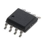
| 描述 | IC EEPROM 4KBIT 20MHZ 8SOIC电可擦除可编程只读存储器 4K (512 X 8) SPI, 1.8V |
| 产品分类 | |
| 品牌 | Atmel |
| 产品手册 | |
| 产品图片 |
|
| rohs | 符合RoHS无铅 / 符合限制有害物质指令(RoHS)规范要求 |
| 产品系列 | 内存,电可擦除可编程只读存储器,Atmel AT25040B-SSHL-T- |
| 数据手册 | |
| 产品型号 | AT25040B-SSHL-T |
| 产品种类 | 电可擦除可编程只读存储器 |
| 供应商器件封装 | 8-SOIC |
| 其它名称 | AT25040B-SSHL-TCT |
| 包装 | 剪切带 (CT) |
| 商标 | Atmel |
| 存储器类型 | EEPROM |
| 存储容量 | 4K (512 x 8) |
| 安装风格 | SMD/SMT |
| 封装 | Reel |
| 封装/外壳 | 8-SOIC(0.154",3.90mm 宽) |
| 封装/箱体 | SOIC-8 |
| 工作温度 | -40°C ~ 85°C |
| 工作电流 | 8.5 mA |
| 工作电源电压 | 1.8 V to 5.5 V |
| 工厂包装数量 | 4000 |
| 接口 | SPI 串行 |
| 接口类型 | SPI |
| 数据保留 | 100 yr |
| 最大工作温度 | + 85 C |
| 最大工作电流 | 10 mA |
| 最大时钟频率 | 20 MHz |
| 最小工作温度 | - 40 C |
| 标准包装 | 1 |
| 格式-存储器 | EEPROMs - 串行 |
| 电压-电源 | 1.8 V ~ 5.5 V |
| 电源电压-最大 | 5.5 V |
| 电源电压-最小 | 1.8 V |
| 组织 | 512 x 8 |
| 速度 | 20MHz |


_renders/IS66WVE4M16EBLL-70BLI.jpg)


- 商务部:美国ITC正式对集成电路等产品启动337调查
- 曝三星4nm工艺存在良率问题 高通将骁龙8 Gen1或转产台积电
- 太阳诱电将投资9.5亿元在常州建新厂生产MLCC 预计2023年完工
- 英特尔发布欧洲新工厂建设计划 深化IDM 2.0 战略
- 台积电先进制程称霸业界 有大客户加持明年业绩稳了
- 达到5530亿美元!SIA预计今年全球半导体销售额将创下新高
- 英特尔拟将自动驾驶子公司Mobileye上市 估值或超500亿美元
- 三星加码芯片和SET,合并消费电子和移动部门,撤换高东真等 CEO
- 三星电子宣布重大人事变动 还合并消费电子和移动部门
- 海关总署:前11个月进口集成电路产品价值2.52万亿元 增长14.8%


PDF Datasheet 数据手册内容提取
AT25010B, AT25020B, AT25040B SPI Serial EEPROM 1K (128x8), 2K (256x8), 4K (512x8) DATASHEET Features Serial Peripheral Interface (SPI) Compatible Supports SPI Modes 0 (0,0) and 3 (1,1) ̶ Data Sheet Describes Mode 0 Operation Low-voltage and Standard-voltage Operation ̶ V = 1.8V to 5.5V CC 20MHz Clock Rate (5V) 8-byte Page Mode Block Write Protection ̶ Protect 1/4, 1/2, or Entire Array Write Protect (WP) Pin and Write Disable Instructions for Both Hardware and Software Data Protection Self-timed Write Cycle (5ms max) High Reliability ̶ Endurance: 1,000,000 Write Cycles ̶ Data Retention: 100 Years Green (Pb/Halogen-free/RoHS Compliant) Packaging Options Die Sales: Wafer Form, Waffle Pack, and Bumped Wafers Description The Atmel® AT25010B/020B/040B provides 1,024/2,048/4,096 bits of Serial Electrically Erasable Programmable Read-Only Memory (EEPROM) organized as 128/256/512 words of 8 bits each. The device is optimized for use in many industrial and commercial applications where low-power and low-voltage operation are essential. The AT25010B/020B/040B is available in space saving, JEDEC SOIC, UDFN, TSSOP, XDFN, and VFBGA packages. The AT25010B/020B/040B is enabled through the Chip Select pin (CS) and accessed via a 3-Wire interface consisting of Serial Data Input (SI), Serial Data Output (SO), and Serial Clock (SCK). All programming cycles are completely self-timed, and no separate erase cycle is required before write. Block Write protection is enabled by programming the status register with one of four blocks of Write Protection. Separate Program Enable and Program Disable instructions are provided for additional data protection. Hardware Data Protection is provided via the WP pin to protect against inadvertent write attempts. The HOLD pin may be used to suspend any serial communication without resetting the serial sequence. Atmel-8707F-SEEPROM-AT25010B-020B-040B-Datasheet_012015
1. Pin Configurations Table 1-1. Pin Configurations 8-lead SOIC 8-lead TSSOP Pin Name Function CS Chip Select CS 1 8 VCC CS 1 8 V CC SO 2 7 HOLD SO 2 7 HOLD SCK Serial Data Clock WP 3 6 SCK WP 3 6 SCK GND 4 5 SI SI Serial Data Input GND 4 5 SI Top View SO Serial Data Output Top View GND Ground V Power Supply CC 8-pad UDFN/XDFN 8-ball VFBGA WP Write Protect V 8 1 CS V 8 1 CS HOLD Suspends Serial Input CC CC HOLD 7 2 SO HOLD 7 2 SO SCK 6 3 WP SCK 6 3 WP SI 5 4 GND SI 5 4 GND Bottom View Bottom View Note: Drawings are not to scale. 2. Absolute Maximum Ratings* Operating Temperature . . . . . . . . . . -40C to + 125C *Notice: Stresses beyond those listed under “Absolute Maximum Ratings” may cause permanent Storage Temperature. . . . . . . . . . . . -65C to + 150C damage to the device. This is a stress rating only and functional operation of the device at Voltage on any pin these or any other conditions beyond those with respect to ground . . . . . . . . . . . . . . . .-1V to + 7V indicated in the operational sections of this specification is not implied. Exposure to Maximum Operating Voltage . . . . . . . . . . . . . . . 6.25V absolute maximum rating conditions for DC Output Current. . . . . . . . . . . . . . . . . . . . . . . . 5mA extended periods may affect device reliability. 2 AT25010B/020B/040B [DATASHEET] Atmel-8707F-SEEPROM-AT25010B-020B-040B-Datasheet_012015
3. Block Diagram Figure 3-1. Block Diagram V CC Status Memory Array Address Register 128/256/512 x 8 Decoder Data Register Output Buffer Mode Decode Logic Clock Generator AT25010B/020B/040B [DATASHEET] 3 Atmel-8707F-SEEPROM-AT25010B-020B-040B-Datasheet_012015
4. Electrical Characteristics 4.1 Pin Capacitance Table 4-1. Pin Capacitance(1) Applicable over recommended operating range from T = 25°C, f = 1MHz, V = +5V (unless otherwise noted). A CC Symbol Test Conditions Max Units Conditions C Output Capacitance (SO) 8 pF V = 0V OUT OUT C Input Capacitance (CS, SCK, SI, WP, HOLD) 6 pF V = 0V IN IN Note: 1. This parameter is characterized and is not 100% tested. 4.2 DC Characteristics Table 4-2. DC Characteristics Applicable over recommended operating range from: T = -40C to +85C, V = +1.8V to +5.5V, (unless otherwise noted). AI CC Symbol Parameter Test Condition Min Typ Max Units V Supply Voltage 1.8 5.5 V CC1 V Supply Voltage 2.5 5.5 V CC2 V Supply Voltage 4.5 5.5 V CC3 V = 5V at 20MHz I Supply Current CC 8.5 10 mA CC1 SO = Open, Read V = 5V at 10MHz I Supply Current CC 4.5 5 mA CC2 SO = Open, Read, Write V = 5V at 1MHz I Supply Current CC 2 3 mA CC3 SO = Open, Read, Write I Standby Current V = 1.8V, CS = V 0.1 0.5 μA SB1 CC CC I Standby Current V = 2.5V, CS = V 0.2 1 μA SB2 CC CC I Standby Current V = 5V, CS = V 2 3.5 μA SB3 CC CC I Input Leakage V = 0V to V 3 μA IL IN CC V = 0V to V I Output Leakage IN CC 3 3 μA OL T = 0°C to 70°C AC V (1) Input Low-voltage 0.6 V x 0.3 V IL CC V (1) Input High-voltage V x 0.7 V + 0.5 V IH CC CC V Output Low-voltage 3.6V V 5.5V I = 3mA 0.4 V OL1 CC OL V Output High-voltage 3.6V V 5.5V I = 1.60mA V 0.8 V OH1 CC OH CC V Output Low-voltage 1.8V V 3.6V I = 0.15mA 0.2 V OL2 CC OL V Output High-voltage 1.8V V 3.6V I = 100μA V 0.2 V OH2 CC OH CC Note: 1. V min and V max are reference only and are not tested. IL IH 4 AT25010B/020B/040B [DATASHEET] Atmel-8707F-SEEPROM-AT25010B-020B-040B-Datasheet_012015
4.3 AC Characteristics Table 4-3. AC Characteristics Applicable over recommended operating range from T = -40 to +85°C, V = As Specified, CL = 1 TTL Gate and 30pF AI CC (unless otherwise noted). Symbol Parameter Voltage Min Max Units 4.5 5.5 0 20 f SCK Clock Frequency 2.5 5.5 0 10 MHz SCK 1.8 5.5 0 5 4.5 5.5 2 t Input Rise Time 2.5 5.5 2 μs RI 1.8 5.5 2 4.5 5.5 2 t Input Fall Time 2.5 5.5 2 μs FI 1.8 5.5 2 4.5 5.5 20 t SCK High Time 2.5 5.5 40 ns WH 1.8 5.5 80 4.5 5.5 20 t SCK Low Time 2.5 5.5 40 ns WL 1.8 5.5 80 4.5 5.5 100 t CS High Time 2.5 5.5 100 ns CS 1.8 5.5 200 4.5 5.5 100 t CS Setup Time 2.5 5.5 100 ns CSS 1.8 5.5 200 4.5 5.5 100 t CS Hold Time 2.5 5.5 100 ns CSH 1.8 5.5 200 4.5 5.5 20 t Data In Setup Time 2.5 5.5 40 ns SU 1.85.5 80 4.5 5.5 20 t Data In Hold Time 2.5 - 5.5 40 ns H 1.8 - 5.5 80 4.5 5.5 20 t Hold Setup Time 2.5 5.5 40 ns HD 1.8 5.5 80 4.5 5.5 20 t Hold Hold Time 2.5 5.5 40 ns CD 1.8 5.5 80 4.5 5.5 0 20 t Output Valid 2.5 5.5 0 40 ns V 1.8 5.5 0 80 4.5 5.5 0 t Output Hold Time 2.5 5.5 0 ns HO 1.8 5.5 0 AT25010B/020B/040B [DATASHEET] 5 Atmel-8707F-SEEPROM-AT25010B-020B-040B-Datasheet_012015
Table 4-3. AC Characteristics (Continued) Applicable over recommended operating range from T = -40 to +85°C, V = As Specified, CL = 1 TTL Gate and 30pF AI CC (unless otherwise noted). Symbol Parameter Voltage Min Max Units 4.5 5.5 0 25 t Hold to Output Low Z 2.5 5.5 0 50 ns LZ 1.8 5.5 0 100 4.5 5.5 25 t Hold to Output High Z 2.5 5.5 50 ns HZ 1.8 5.5 100 4.5 5.5 25 t Output Disable Time 2.5 5.5 50 ns DIS 1.8 5.5 100 4.5 5.5 5 t Write Cycle Time 2.5 5.5 5 ms WC 1.8 5.5 5 Endurance(1) 5V, 25C, Page Mode 1,000,000 Write Cycles Note: 1. This parameter is characterized and is not 100% tested. 5. Serial Interface Description Master: The device that generates the serial clock. Slave: Because the Serial Clock pin (SCK) is always an input, the AT25010B/020B/040B always operates as a slave. Transmitter/Receiver: The AT25010B/020B/040B has separate pins designated for data transmission (SO) and reception (SI). MSB: The Most Significant Bit (MSB) is the first bit transmitted and received. Serial Opcode: After the device is selected with CS going low, the first byte will be received. This byte contains the opcode which defines the operations to be performed. The opcode also contains address bit A8 in both the read and write instructions for the AT25040B. Invalid Opcode: If an invalid opcode is received, no data will be shifted into the AT25010B/020B/040B, and the serial output pin (SO) will remain in a high-impedance state until the falling edge of CS is detected again. This will reinitialize the serial communication. Chip Select: The AT25010B/020B/040B is selected when the CS pin is low. When the device is not selected, data will not be accepted via the SI pin, and the SO pin will remain in a high impedance state. Hold: The HOLD pin is used in conjunction with the CS pin to select the AT25010B/020B/040B. When the device is selected and a serial sequence is underway, HOLD can be used to pause the serial communication with the master device without resetting the serial sequence. To pause, the HOLD pin must be brought low while the SCK pin is low. To resume serial communication, the HOLD pin is brought high while the SCK pin is low (SCK may still toggle during HOLD). Inputs to the SI pin will be ignored while the SO pin is in the high impedance state. Write Protect: The write protect pin (WP) will allow normal read/write operations when held high. When the WP pin is brought low, all write operations are inhibited. WP going low while CS is still low will interrupt a write to the AT25010B/020B/040B. If the internal write cycle has already been initiated, WP going low will have no effect on any write operation. 6 AT25010B/020B/040B [DATASHEET] Atmel-8707F-SEEPROM-AT25010B-020B-040B-Datasheet_012015
Figure 5-1. SPI Serial Interface Master: Slave: Microcontroller AT25010B/020B/040B Data Out (MOSI) SI Data In (MISO) SO Serial Clock (SPI CK) SCK SS0 CS SS1 SI SS2 SO SS3 SCK CS SI SO SCK CS SI SO SCK CS AT25010B/020B/040B [DATASHEET] 7 Atmel-8707F-SEEPROM-AT25010B-020B-040B-Datasheet_012015
6. Functional Description The AT25010B/020B/040B is designed to interface directly with the synchronous Serial Peripheral Interface (SPI) of the 6805 and 68HC11 series of microcontrollers. The AT25010B/020B/040B utilizes an 8-bit instruction register. The list of instructions and their operation codes are contained in Figure 6-1. All instructions, addresses, and data are transferred with the MSB first and start with a high-to-low CS transition. Table 6-1. Instruction Set for the AT25010B/020B/040B Instruction Name Instruction Format Operation WREN 0000 X110 Set Write Enable Latch WRDI 0000 X100 Reset Write Enable Latch RDSR 0000 X101 Read Status Register WRSR 0000 X001 Write Status Register READ 0000 A011 Read Data from Memory Array WRITE 0000 A010 Write Data to Memory Array Note: 1. “A” represents MSB address bit A8 for the AT25040B. Write Enable (WREN): The device will power-up in the Write Disable state when V is applied. All CC programming instructions must therefore be preceded by a Write Enable instruction. The WP pin must be held high during a WREN instruction. Write Disable (WRDI): To protect the device against inadvertent writes, the Write Disable instruction disables all programming modes. The WRDI instruction is independent of the status of the WP pin. Read Status Register (RDSR): The Read Status Register instruction provides access to the status register. The Read/Busy and Write Enable status of the device can be determined by the RDSR instruction. Similarly, the Block Write Protection bits indicate the extent of protection employed. These bits are set by using the WRSR instruction. Table 6-2. Status Register Format Bit 7 Bit 6 Bit 5 Bit 4 Bit 3 Bit 2 Bit 1 Bit 0 X X X X BP1 BP0 WEN RDY Table 6-3. Read Status Register Bit Definition Bit Definition Bit 0 = 0 (RDY) indicates the device is ready. Bit 0 (RDY) Bit 0 = 1 indicates the write cycle is in progress. Bit 1 = 0 indicates the device is not write enabled. Bit 1 (WEN) Bit 1 = 1 indicates the device is write enabled. Bit 2 (BP0) See Table 6-4. Bit 3 (BP1) See Table 6-4. Bits 4 – 7 are zeros when device is not in an internal write cycle. Bits 0 – 7 are ones during an internal write cycle. 8 AT25010B/020B/040B [DATASHEET] Atmel-8707F-SEEPROM-AT25010B-020B-040B-Datasheet_012015
Write Status Register (WRSR): The WRSR instruction allows the user to select one of four levels of protection. The AT25010B/020B/040B is divided into four array segments. None, one-quarter (¼), one-half (½), or all of the memory segments can be protected. Any of the data within any selected segment will therefore be read-only. The block write protection levels and corresponding status register control bits are shown in Table 6-4. Bits BP1 and BP0 are nonvolatile cells that have the same properties and functions as the regular memory cells (e.g., WREN, t , RDSR). WC Table 6-4. Block Write Protect Bits Status Register Bits Array Addresses Protected Level BP1 BP0 AT25010B AT25020B AT25040B 0 0 0 None None None 1 (¼) 0 1 607F C0 FF 180 FF 2 (½) 1 0 40 7F 80 FF 100 1FF 3 (All) 1 1 00 7F 00 FF 000 1FF Read Sequence (READ): Reading the AT25010B/020B/040B via the SO pin requires the following sequence. After the CS line is pulled low to select a device, the Read opcode (including A8 for the AT25040B) is transmitted via the SI line followed by the byte address to be read (A7 A0). Upon completion, any data on the SI line will be ignored. The data (D7 D0) at the specified address is then shifted out onto the SO line. If only one byte is to be read, the CS line should be driven high after the data comes out. The Read Sequence can be continued since the byte address is automatically incremented and data will continue to be shifted out. When the highest address is reached, the address counter will roll-over to the lowest address allowing the entire memory to be read in one continuous read cycle. Write Sequence (WRITE): In order to program the AT25010B/020B/040B, the Write Protect pin (WP) must be held high and two separate instructions must be executed. First, the device must be write enabled via the WREN instruction. Then a Write (WRITE) instruction may be executed. Also, the address of the memory location(s) to be programmed must be outside the protected address field location selected by the Block Write Protection level. During an internal write cycle, all commands will be ignored except the RDSR instruction. A Write instruction requires the following sequence. After the CS line is pulled low to select the device, the Write opcode (including A8 for the AT25040B) is transmitted via the SI line followed by the byte address (A7 A0) and the data (D7 D0) to be programmed. Programming will start after the CS pin is brought high. The low-to-high transition of the CS pin must occur during the SCK low time immediately after clocking in the D0 (LSB) data bit. The Ready/Busy status of the device can be determined by initiating a Read Status Register (RDSR) instruction. If Bit 0 = 1, the write cycle is still in progress. If Bit 0 = 0, the write cycle has ended. Only the RDSR instruction is enabled during the write programming cycle. The AT25010B/020B/040B is capable of an 8-byte Page Write operation. After each byte of data is received, the three low-order address bits are internally incremented by one; the six high-order bits of the address will remain constant. If more than eight bytes of data are transmitted, the address counter will roll-over and the previously written data will be overwritten. The AT25010B/020B/040B is automatically returned to the Write Disable state at the completion of a write cycle. Note: If the WP pin is brought low or if the device is not Write Enabled (WREN), the device will ignore the Write instruction and will return to the standby state, when CS is brought high. A new CS falling edge is required to reinitiate the serial communication. AT25010B/020B/040B [DATASHEET] 9 Atmel-8707F-SEEPROM-AT25010B-020B-040B-Datasheet_012015
7. Timing Diagrams Figure 7-1. Synchronous Data Timing (for Mode 0) t V CS IH CS V IL tCSS tCSH V IH SCK t t WH WL V IL t t SU H V IH SI Valid In V IL tV tHO tDIS V OH HI-Z HI-Z SO V OL Figure 7-2. WREN Timing CS SCK SI WREN Opcode HI-Z SO Figure 7-3. WRDI Timing CS SCK SI WRDI Opcode HI-Z SO 10 AT25010B/020B/040B [DATASHEET] Atmel-8707F-SEEPROM-AT25010B-020B-040B-Datasheet_012015
Figure 7-4. RDSR Timing CS 0 1 2 3 4 5 6 7 8 9 10 11 12 13 14 15 SCK SI Instruction Data Out High-impedance SO 7 6 5 4 3 2 1 0 MSB Figure 7-5. WRSR Timing CS 0 1 2 3 4 5 6 7 8 9 10 11 12 13 14 15 SCK Data In SI Instruction 7 6 5 4 3 2 1 0 High-impedance SO Figure 7-6. READ Timing CS 0 1 2 3 4 5 6 7 8 9 10 11 12 13 14 15 16 17 18 19 20 21 22 23 SCK Instruction Byte Address SI 8 7 6 5 4 3 2 1 0 9th bit of Address Data Out SO High-impedance 7 6 5 4 3 2 1 0 MSB AT25010B/020B/040B [DATASHEET] 11 Atmel-8707F-SEEPROM-AT25010B-020B-040B-Datasheet_012015
Figure 7-7. WRITE Timing CS 0 1 2 3 4 5 6 7 8 9 10 11 12 13 14 15 16 17 18 19 20 21 22 23 SCK Instruction Byte Address Data In SI 8 7 6 5 4 3 2 1 0 7 6 5 4 3 2 1 0 9th bit of Address SO High-impedance Figure 7-8. HOLD Timing CS t t CD CD SCK t HD HOLD t HD t HZ SO t LZ 12 AT25010B/020B/040B [DATASHEET] Atmel-8707F-SEEPROM-AT25010B-020B-040B-Datasheet_012015
8. Ordering Code Detail A T 2 5 0 1 0 B - S S H L - B Atmel Designator Shipping Carrier Option B = Bulk (Tubes) T = Tape and Reel, Standard Quantity Option E = Tape and Reel, Expanded Quantity Option Product Family 25 = Standard SPI Serial EPPROM Operating Voltage M = 1.8V to 5.5V Device Density Package Device Grade or 010 = 1k 020 = 2k Wafer/Die Thickness 040 = 4k H = Green, NiPdAu Lead Finish, Industrial Temperature Range (-40˚C to +85˚C) Device Revision U = Green, Matte Sn Lead Finish, Industrial Temperature Range (-40˚C to +85˚C) 11 = 11mil Wafer Thickness Package Option SS = JEDEC SOIC X = TSSOP MA = UDFN ME = XDFN C = VFBGA WWU = Wafer unsawn WDT = Die in Tape and Reel AT25010B/020B/040B [DATASHEET] 13 Atmel-8707F-SEEPROM-AT25010B-020B-040B-Datasheet_012015
9. Part Markings AT25010B, AT25020B and AT25040B: Package Marking Information 8-lead SOIC 8-lead TSSOP 8-pad UDFN 2.0 x 3.0 mm Body ATHYWW ### ATMLHYWW ###% @ ###% @ H%@ AAAAAAAA AAAAAAA YXX 8-ball VFBGA 8-pad XDFN 1.5 x 2.0 mm Body 1.8 x 2.2 mm Body ###U ### YMXX YXX PIN 1 Note 1: designates pin 1 Note 2: Package drawings are not to scale Catalog Number Truncation AT25010B Truncation Code ###: 51B AT25020B Truncation Code ###: 52B AT25040B Truncation Code ###: 54B Date Codes Voltages Y = Year M = Month WW = Work Week of Assembly % = Minimum Voltage 4: 2014 8: 2018 A: January 02: Week 2 L: 1.8V min 5: 2015 9: 2019 B: February 04: Week 4 6: 2016 0: 2020 ... ... 7: 2017 1: 2021 L: December 52: Week 52 Country of Assembly L ot Number Grade/Lead Finish Material @ = Country of Assembly AAA...A = Atmel Wafer Lot Number H: Industrial/NiPdAu U: Industrial/Matte Tin/SnAgCu Trace Code Atmel Truncation XX = Trace Code (Atmel Lot Numbers Correspond to Code) AT: Atmel Example: AA, AB.... YZ, ZZ ATM: Atmel ATML: Atmel 1/15/14 TITLE DRAWING NO. REV. Package Mark Contact: 25010-02-04BSM, AT25010B, AT25020B and AT25040B 25010-02-04BSM B DL-CSO-Assy_eng@atmel.com Package Marking Information 14 AT25010B/020B/040B [DATASHEET] Atmel-8707F-SEEPROM-AT25010B-020B-040B-Datasheet_012015
10. Ordering Information Delivery Information Operation Atmel Ordering Code Lead Finish Package Form Quantity Range AT25010B-SSHL-B Bulk (Tubes) 100 per Tube 8S1 AT25010B-SSHL-T Tape and Reel 4,000 per Reel AT25010B-XHL-B Bulk (Tubes) 100 per Tube 8X NiPdAu AT25010B-XHL-T Tape and Reel 5,000 per Reel (Lead-free/Halogen-free) Industrial AT25010B-MAHL-T Tape and Reel 5,000 per Reel Temperature 8MA2 AT25010B-MAHL-E Tape and Reel 15,000 per Reel (-40 to 85C) AT25010B-MEHL-T 8ME1 Tape and Reel 5,000 per Reel SnAgCu AT25010B-CUL-T 8U3-1 Tape and Reel 5,000 per Reel (Lead-free/Halogen-free) AT25010B-WWU11L (1) N/A Wafer Note 1 AT25020B-SSHL-B Bulk (Tubes) 100 per Tube 8S1 AT25020B-SSHL-T Tape and Reel 4,000 per Reel AT25020B-XHL-B Bulk (Tubes) 100 per Tube 8X NiPdAu AT25020B-XHL-T Tape and Reel 5,000 per Reel (Lead-free/Halogen-free) Industrial AT25020B-MAHL-T Tape and Reel 5,000 per Reel Temperature 8MA2 AT25020B-MAHL-E Tape and Reel 15,000 per Reel (-40 to 85C) AT25020B-MEHL-T 8ME1 Tape and Reel 5,000 per Reel SnAgCu AT25020B-CUL-T 8U3-1 Tape and Reel 5,000 per Reel (Lead-free/Halogen-free) AT25020B-WWU11L (1) N/A Wafer Note 1 AT25040B-SSHL-B Bulk (Tubes) 100 per Tube 8S1 AT25040B-SSHL-T Tape and Reel 4,000 per Reel AT25040B-XHL-B Bulk (Tubes) 100 per Tube 8X NiPdAu AT25040B-XHL-T Tape and Reel 5,000 per Reel (Lead-free/Halogen-free) Industrial AT25040B-MAHL-T Tape and Reel 5,000 per Reel Temperature 8MA2 AT25040B-MAHL-E Tape and Reel 15,000 per Reel (-40 to 85C) AT25040B-MEHL-T 8ME1 Tape and Reel 5,000 per Reel SnAgCu AT25040B-CUL-T 8U3-1 Tape and Reel 5,000 per Reel (Lead-free/Halogen-free) AT25040B-WWU11L (1) N/A Wafer Note 1 Note: 1. Contact Atmel Sales for Wafer sales. AT25010B/020B/040B [DATASHEET] 15 Atmel-8707F-SEEPROM-AT25010B-020B-040B-Datasheet_012015
Package Type 8S1 8-lead, 0.15" wide, Plastic Gull Wing Small Outline (JEDEC SOIC) 8X 8-lead, 4.40mm body, Plastic Thin Shrink Small Outline Package (TSSOP) 8MA2 8-pad, 2.00mm x 3.00mm body, 0.50mm pitch, Plastic Ultra Thin Dual Flat No Lead (UDFN) 8ME1 8-pad, 1.80mm x 2.20mm body, 0.40mm pitch, Extra Thin Dual Flat No Lead (XDFN) 8U3-1 8-ball, 1.50mm x 2.00mm body, 0.50mm pitch, Die Ball Grid Array (VFBGA) 16 AT25010B/020B/040B [DATASHEET] Atmel-8707F-SEEPROM-AT25010B-020B-040B-Datasheet_012015
11. Packaging Information 11.1 8S1 — 8-lead JEDEC SOIC C 1 E E1 L N Ø TOP VIEW END VIEW e b A COMMON DIMENSIONS (Unit of Measure = mm) SYMBOL MIN NOM MAX NOTE A1 A 1.35 – 1.75 A1 0.10 – 0.25 b 0.31 – 0.51 C 0.17 – 0.25 D 4.80 – 5.05 D E1 3.81 – 3.99 E 5.79 – 6.20 SIDE VIEW e 1.27 BSC Notes: This drawing is for general information only. L 0.40 – 1.27 Refer to JEDEC Drawing MS-012, Variation AA ØØ 0° – 8° for proper dimensions, tolerances, datums, etc. 6/22/11 TITLE GPC DRAWING NO. REV. 8S1, 8-lead (0.150” Wide Body), Plastic Gull Wing SWB 8S1 G Package Drawing Contact: Small Outline (JEDEC SOIC) packagedrawings@atmel.com AT25010B/020B/040B [DATASHEET] 17 Atmel-8707F-SEEPROM-AT25010B-020B-040B-Datasheet_012015
11.2 8X — 8-lead TSSOP C 1 Pin 1 indicator this corner E1 E L1 N L Top View End View A b A1 COMMON DIMENSIONS e A2 (Unit of Measure = mm) D SYMBOL MIN NOM MAX NOTE Side View A - - 1.20 A1 0.05 - 0.15 Notes: 1. This drawing is for general information only. A2 0.80 1.00 1.05 Refer to JEDEC Drawing MO-153, Variation AA, for proper dimensions, tolerances, datums, etc. D 2.90 3.00 3.10 2, 5 2. Dimension D does not include mold Flash, protrusions or gate E 6.40 BSC burrs. Mold Flash, protrusions and gate burrs shall not exceed 0.15mm (0.006in) per side. E1 4.30 4.40 4.50 3, 5 3. Dimension E1 does not include inter-lead Flash or protrusions. Inter-lead Flash and protrusions shall not exceed 0.25mm b 0.19 0.25 0.30 4 (0.010in) per side. e 0.65 BSC 4. Dimension b does not include Dambar protrusion. Allowable Dambar protrusion shall be 0.08mm total in excess L 0.45 0.60 0.75 of the b dimension at maximum material condition. Dambar L1 1.00 REF cannot be located on the lower radius of the foot. Minimum space between protrusion and adjacent lead is 0.07mm. C 0.09 - 0.20 5. Dimension D and E1 to be determined at Datum Plane H. 2/27/14 TITLE GPC DRAWING NO. REV. 8X, 8-lead 4.4mm Body, Plastic Thin Package Drawing Contact: Shrink Small Outline Package (TSSOP) TNR 8X E packagedrawings@atmel.com 18 AT25010B/020B/040B [DATASHEET] Atmel-8707F-SEEPROM-AT25010B-020B-040B-Datasheet_012015
11.3 8MA2 — 8-pad UDFN E 1 8 Pin 1 ID 2 7 D 3 6 4 5 TOP VIEW C SIDE VIEW A2 A A1 E2 b (8x) 8 1 COMMON DIMENSIONS 7 2 Pin#1 ID (Unit of Measure = mm) D2 6 3 SYMBOL MIN NOM MAX NOTE A 0.50 0.55 0.60 5 4 A1 0.0 0.02 0.05 e (6x) A2 - - 0.55 L (8x) K D 1.90 2.00 2.10 BOTTOM VIEW D2 1.40 1.50 1.60 Notes: 1. This drawing is for general information only. Refer to E 2.90 3.00 3.10 Drawing MO-229, for proper dimensions, tolerances, E2 1.20 1.30 1.40 datums, etc. 2. The Pin #1 ID is a laser-marked feature on Top View. b 0.18 0.25 0.30 3 3. Dimensions b applies to metallized terminal and is C 1.52 REF measured between 0.15 mm and 0.30 mm from the terminal tip. If the terminal has the optional radius on L 0.30 0.35 0.40 the other end of the terminal, the dimension should e 0.50 BSC not be measured in that radius area. 4. The Pin #1 ID on the Bottom View is an orientation K 0.20 - - feature on the thermal pad. 11/26/14 TITLE GPC DRAWING NO. REV. 8MA2, 8-pad 2 x 3 x 0.6mm Body, Thermally Package Drawing Contact: Enhanced Plastic Ultra Thin Dual Flat No-Lead YNZ 8MA2 G packagedrawings@atmel.com Package (UDFN) AT25010B/020B/040B [DATASHEET] 19 Atmel-8707F-SEEPROM-AT25010B-020B-040B-Datasheet_012015
11.4 8ME1 — 8-pad XDFN D 8 7 6 5 PIN #1 ID E 1 2 3 4 A1 Top View A Side View e1 b L COMMON DIMENSIONS (Unit of Measure = mm) SYMBOL MIN NOM MAX NOTE 0.10 A – – 0.40 PIN #1 ID A1 0.00 – 0.05 D 1.70 1.80 1.90 0.15 E 2.10 2.20 2.30 b 0.15 0.20 0.25 b e 0.40 TYP e e1 1.20 REF L 0.26 0.30 0.35 End View 9/10/2012 TITLE GPC DRAWING NO. REV. 8ME1, 8-pad (1.80mm x 2.20mm body) Extra Thin DFN DTP 8ME1 B Package Drawing Contact: (XDFN) packagedrawings@atmel.com 20 AT25010B/020B/040B [DATASHEET] Atmel-8707F-SEEPROM-AT25010B-020B-040B-Datasheet_012015
11.5 8U3-1 — 8-ball VFBGA E D 2. b PIN 1 BALL PAD CORNER A1 A2 TOP VIEW A SIDE VIEW PIN 1 BALL PAD CORNER 1 2 3 4 d (d1) 8 7 6 5 e COMMON DIMENSIONS (Unit of Measure - mm) (e1) SYMBOL MIN NOM MAX NOTE BOTTOM VIEW A 0.73 0.79 0.85 8 SOLDER BALLS A1 0.09 0.14 0.19 A2 0.40 0.45 0.50 Notes: b 0.20 0.25 0.30 2 1. This drawing is for general information only. D 1.50 BSC E 2.0 BSC 2. Dimension ‘b’ is measured at maximum solder ball diameter. e 0.50 BSC 3. Solder ball composition shall be 95.5Sn-4.0Ag-.5Cu. e1 0.25 REF d 1.00 BSC d1 0.25 REF 6/11/13 TITLE GPC DRAWING NO. REV. 8U3-1, 8-ball, 1.50mm x 2.00mm body, 0.50mm pitch, Package Drawing Contact: Very Thin, Fine-Pitch Ball Grid Array Package (VFBGA) GXU 8U3-1 F packagedrawings@atmel.com AT25010B/020B/040B [DATASHEET] 21 Atmel-8707F-SEEPROM-AT25010B-020B-040B-Datasheet_012015
12. Revision History Doc. Rev. Date Comments Add the UDFN Expanded Quantity Option. 8707F 01/2015 Update the 8MA2 package outline drawing and the ordering information section. Update part markings, package drawings, package 8A2 to 8X, template, logos, and 8707E 05/2014 disclaimer page. No change to functional specification. Correct WRSR waveform figure 4-5, bit 7 is not writable. 8707D 04/2013 Update Atmel logos and disclaimer page. Correct AT25040B-SSHL marking detail. 8707C 06/2011 Replace 8A2 package drawing with version E. 8707B 10/2010 Remove Preliminary. 8707B 03/2010 Replace 8Y6 with 8MA2. 8707A 02/2010 Initial document release. 22 AT25010B/020B/040B [DATASHEET] Atmel-8707F-SEEPROM-AT25010B-020B-040B-Datasheet_012015
X X X X X X Atmel Corporation 1600 Technology Drive, San Jose, CA 95110 USA T: (+1)(408) 441.0311 F: (+1)(408) 436.4200 | www.atmel.com © 2015 Atmel Corporation. / Rev.: Atmel-8707F-SEEPROM-AT25010B-020B-040B-Datasheet_012015. Atmel®, Atmel logo and combinations thereof, Enabling Unlimited Possibilities®, and others are registered trademarks or trademarks of Atmel Corporation in U.S. and other countries. Other terms and product names may be trademarks of others. DISCLAIMER: The information in this document is provided in connection with Atmel products. No license, express or implied, by estoppel or otherwise, to any intellectual property right is granted by this document or in connection with the sale of Atmel products. EXCEPT AS SET FORTH IN THE ATMEL TERMS AND CONDITIONS OF SALES LOCATED ON THE ATMEL WEBSITE, ATMEL ASSUMES NO LIABILITY WHATSOEVER AND DISCLAIMS ANY EXPRESS, IMPLIED OR STATUTORY WARRANTY RELATING TO ITS PRODUCTS INCLUDING, BUT NOT LIMITED TO, THE IMPLIED WARRANTY OF MERCHANTABILITY, FITNESS FOR A PARTICULAR PURPOSE, OR NON-INFRINGEMENT. IN NO EVENT SHALL ATMEL BE LIABLE FOR ANY DIRECT, INDIRECT, CONSEQUENTIAL, PUNITIVE, SPECIAL OR INCIDENTAL DAMAGES (INCLUDING, WITHOUT LIMITATION, DAMAGES FOR LOSS AND PROFITS, BUSINESS INTERRUPTION, OR LOSS OF INFORMATION) ARISING OUT OF THE USE OR INABILITY TO USE THIS DOCUMENT, EVEN IF ATMEL HAS BEEN ADVISED OF THE POSSIBILITY OF SUCH DAMAGES. Atmel makes no representations or warranties with respect to the accuracy or completeness of the contents of this document and reserves the right to make changes to specifications and products descriptions at any time without notice. Atmel does not make any commitment to update the information contained herein. Unless specifically provided otherwise, Atmel products are not suitable for, and shall not be used in, automotive applications. Atmel products are not intended, authorized, or warranted for use as components in applications intended to support or sustain life. SAFETY-CRITICAL, MILITARY, AND AUTOMOTIVE APPLICATIONS DISCLAIMER: Atmel products are not designed for and will not be used in connection with any applications where the failure of such products would reasonably be expected to result in significant personal injury or death (“Safety-Critical Applications”) without an Atmel officer's specific written consent. Safety-Critical Applications include, without limitation, life support devices and systems, equipment or systems for the operation of nuclear facilities and weapons systems. Atmel products are not designed nor intended for use in military or aerospace applications or environments unless specifically designated by Atmel as military-grade. Atmel products are not designed nor intended for use in automotive applications unless specifically designated by Atmel as automotive-grade.
Mouser Electronics Authorized Distributor Click to View Pricing, Inventory, Delivery & Lifecycle Information: M icrochip: AT25010B-MAHL-T AT25010B-SSHL-B AT25010B-SSHL-T AT25010B-XHL-B AT25010B-XHL-T AT25020B- MAHL-T AT25020B-SSHL-B AT25020B-SSHL-T AT25020B-XHL-B AT25020B-XHL-T AT25040B-MAHL-T AT25040B-SSHL-B AT25040B-SSHL-T AT25040B-XHL-B AT25040B-XHL-T AT25040B-MAHL-E AT25010B-MAHL- E AT25020B-MAHL-E