
 Datasheet下载
- 型号: 25AA320A-I/SN
- 制造商: Microchip
- 库位|库存: xxxx|xxxx
- 要求:
| 数量阶梯 | 香港交货 | 国内含税 |
| +xxxx | $xxxx | ¥xxxx |
查看当月历史价格
查看今年历史价格
25AA320A-I/SN产品简介:
ICGOO电子元器件商城为您提供25AA320A-I/SN由Microchip设计生产,在icgoo商城现货销售,并且可以通过原厂、代理商等渠道进行代购。 25AA320A-I/SN价格参考。Microchip25AA320A-I/SN封装/规格:存储器, EEPROM 存储器 IC 32Kb (4K x 8) SPI 10MHz 8-SOIC。您可以下载25AA320A-I/SN参考资料、Datasheet数据手册功能说明书,资料中有25AA320A-I/SN 详细功能的应用电路图电压和使用方法及教程。
Microchip Technology的25AA320A-I/SN是一款32K位的串行EEPROM存储器,采用SPI接口,具有低功耗、高可靠性的特点,广泛应用于以下场景:

1. 工业控制设备:用于存储配置参数、校准数据或运行记录,如PLC、传感器和测量仪器中。
2. 消费电子产品:如智能家电、穿戴设备,用于保存用户设置或设备状态信息。
3. 通信设备:在路由器、交换机等网络设备中存储配置文件和固件参数。
4. 汽车电子:用于车载系统中保存关键数据,如ECU参数或诊断信息。
5. 医疗设备:存储设备校准数据、使用记录等,确保数据断电不丢失。

其工业级温度范围(-40°C至+85°C)和高耐用性(擦写次数达100万次)使其适应复杂环境。
| 参数 | 数值 |
| 产品目录 | 集成电路 (IC)半导体 |
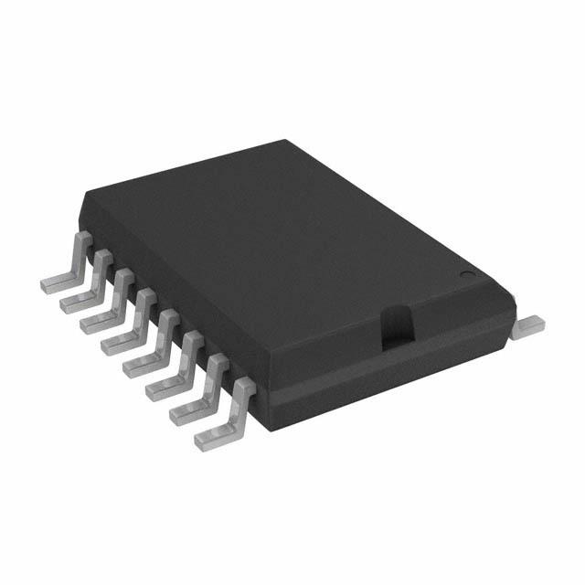
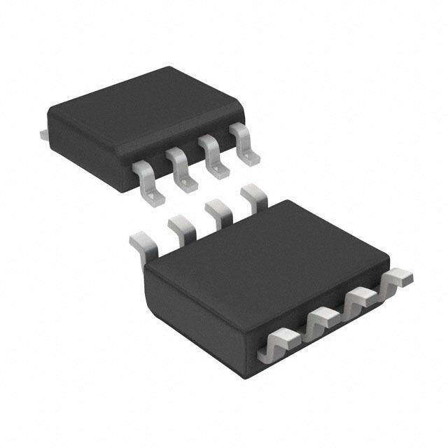
| 描述 | IC EEPROM 32KBIT 10MHZ 8SOIC电可擦除可编程只读存储器 32K 4KX8 1.8V SER EE IND |
| 产品分类 | |
| 品牌 | Microchip Technology |
| 产品手册 | |
| 产品图片 |
|
| rohs | 符合RoHS无铅 / 符合限制有害物质指令(RoHS)规范要求 |
| 产品系列 | 内存,电可擦除可编程只读存储器,Microchip Technology 25AA320A-I/SN- |
| 数据手册 | http://www.microchip.com/mymicrochip/filehandler.aspx?ddocname=en028458 |
| 产品型号 | 25AA320A-I/SN |
| PCN设计/规格 | http://www.microchip.com/mymicrochip/NotificationDetails.aspx?pcn=JAON-29UDMC755&print=view |
| 产品目录页面 | |
| 产品种类 | 电可擦除可编程只读存储器 |
| 供应商器件封装 | 8-SOIC N |
| 其它名称 | 25AA320AISN |
| 包装 | 管件 |
| 商标 | Microchip Technology |
| 存储器类型 | EEPROM |
| 存储容量 | 32K (4K x 8) |
| 安装风格 | SMD/SMT |
| 封装 | Tube |
| 封装/外壳 | 8-SOIC(0.154",3.90mm 宽) |
| 封装/箱体 | SOIC-8 |
| 工作温度 | -40°C ~ 85°C |
| 工作电流 | 5 mA |
| 工作电源电压 | 2.5 V, 3.3 V, 5 V |
| 工厂包装数量 | 100 |
| 接口 | SPI 串行 |
| 接口类型 | SPI |
| 数据保留 | 200 yr |
| 最大工作温度 | + 85 C |
| 最大工作电流 | 5 mA |
| 最大时钟频率 | 10 MHz |
| 最小工作温度 | - 40 C |
| 标准包装 | 100 |
| 格式-存储器 | EEPROMs - 串行 |
| 电压-电源 | 1.8 V ~ 5.5 V |
| 电源电压-最大 | 5.5 V |
| 电源电压-最小 | 1.8 V |
| 组织 | 4 k x 8 |
| 访问时间 | 50 ns |
| 速度 | 10MHz |


- 商务部:美国ITC正式对集成电路等产品启动337调查
- 曝三星4nm工艺存在良率问题 高通将骁龙8 Gen1或转产台积电
- 太阳诱电将投资9.5亿元在常州建新厂生产MLCC 预计2023年完工
- 英特尔发布欧洲新工厂建设计划 深化IDM 2.0 战略
- 台积电先进制程称霸业界 有大客户加持明年业绩稳了
- 达到5530亿美元!SIA预计今年全球半导体销售额将创下新高
- 英特尔拟将自动驾驶子公司Mobileye上市 估值或超500亿美元
- 三星加码芯片和SET,合并消费电子和移动部门,撤换高东真等 CEO
- 三星电子宣布重大人事变动 还合并消费电子和移动部门
- 海关总署:前11个月进口集成电路产品价值2.52万亿元 增长14.8%


PDF Datasheet 数据手册内容提取
25AA320A/25LC320A 32K SPI Bus Serial EEPROM Device Selection Table Part Number VCC Range Page Size Temp. Ranges Packages 25LC320A 2.5-5.5V 32 Byte I,E P, SN, ST, MS, MNY 25AA320A 1.8-5.5V 32 Byte I P, SN, ST, MS, MNY Features Description • Max. Clock 10 MHz The Microchip Technology Inc. 25AA320A/25LC320A • Low-Power CMOS Technology: (25XX320A*) are 32 kbit Serial Electrically Erasable PROMs. The memory is accessed via a simple Serial - Max. Write Current: 5 mA at 5.5V, 10 MHz Peripheral Interface (SPI) compatible serial bus. The - Read Current: 5 mA at 5.5V, 10 MHz bus signals required are a clock input (SCK) plus sep- - Standby Current: 5 A at 5.5V arate data in (SI) and data out (SO) lines. Access to the • 4096 x 8-bit Organization device is controlled through a Chip Select (CS) input. • 32-Byte Page Communication to the device can be paused via the • Self-Timed Erase and Write Cycles (5 ms max.) hold pin (HOLD). While the device is paused, transi- • Block Write Protection: tions on its inputs will be ignored, with the exception of - Protect none, 1/4, 1/2 or all of array Chip Select, allowing the host to service higher priority interrupts. • Built-in Write Protection: - Power-on/off data protection circuitry The 25XX320A is available in standard packages including 8-lead PDIP and SOIC, and advanced - Write enable latch packaging including 8-lead MSOP, TSSOP and 2x3 - Write-protect pin TDFN. • Sequential Read • High Reliability: Package Types (not to scale) - Endurance: >1M erase/write cycles TSSOP/MSOP PDIP/SOIC - Data retention: > 200 years (ST, MS) (P, SN) - ESD protection: > 4000V • Temperature Ranges Supported: CS 1 8 VCC CS 1 8 VCC - Industrial (I): -40C to +85C SO 2 7 HOLD SO 2 7 HOLD - Extended (E): -40°C to +125°C VWSPS 34 65 SSCIK WP 3 6 SCK • Pb-Free and RoHS Compliant VSS 4 5 SI • Automotive AECQ-100 Qualified X-Rotated TSSOP TDFN (X/ST) (MNY) HOLD 1 8 SCK CS 1 8 VCC VCC 2 7 SI SO 2 7 HOLD CS 3 6 VSS WP 3 6 SCK SO 4 5 WP VSS 4 5 SI *25XX320A is used in this document as a generic part number for the 25AA320A, 25LC320A devices. 2007-2018 Microchip Technology Inc. DS20001828G-page 1
25AA320A/25LC320A 1.0 ELECTRICAL CHARACTERISTICS Absolute Maximum Ratings(†) VCC.............................................................................................................................................................................6.5V All inputs and outputs w.r.t. VSS.........................................................................................................-0.6V to VCC +1.0V Storage temperature.................................................................................................................................-65°C to 150°C Ambient temperature under bias...............................................................................................................-65°C to 125°C ESD protection on all pins..........................................................................................................................................4 kV † NOTICE: Stresses above those listed under “Absolute Maximum Ratings” may cause permanent damage to the device. This is a stress rating only and functional operation of the device at those or any other conditions above those indicated in the operational listings of this specification is not implied. Exposure to maximum rating conditions for an extended period of time may affect device reliability. TABLE 1-1: DC CHARACTERISTICS Industrial (I): TA = -40°C to +85°C VCC = 1.8V to 5.5V DC CHARACTERISTICS Automotive (E): TA = -40°C to +125°C VCC = 2.5V to 5.5V Param. Sym. Characteristic Min. Max. Units Test Conditions No. D001 VIH1 High-level input .7 VCC VCC+1 V voltage D002 VIL1 Low-level input -0.3 0.3VCC V VCC2.7V D003 VIL2 voltage -0.3 0.2VCC V VCC < 2.7V D004 VOL Low-level output — 0.4 V IOL = 2.1 mA D005 VOL voltage — 0.2 V IOL = 1.0 mA, VCC < 2.5V D006 VOH High-level output VCC -0.5 — V IOH = -400 A voltage D007 ILI Input leakage current — ±1 A CS = VCC, VIN = VSS TO VCC D008 ILO Output leakage — ±1 A CS = VCC, VOUT = VSS TO VCC current D009 CINT Internal Capacitance — 7 pF TA = 25°C, CLK = 1.0 MHz, (all inputs and VCC = 5.0V (Note) outputs) D010 ICC Read — 5 mA VCC = 5.5V; FCLK = 10.0 MHz; — SO = Open Operating Current 2.5 mA VCC = 2.5V; FCLK = 5.0 MHz; SO = Open D011 ICC Write — 5 mA VCC = 5.5V — 3 mA VCC = 2.5V D012 ICCS — 5 A CS = VCC = 5.5V, Inputs tied to VCC or Standby Current — VSS, 125°C 1 A CS = VCC = 5.5V, Inputs tied to VCC or VSS, 85°C Note: This parameter is periodically sampled and not 100% tested. 2007-2018 Microchip Technology Inc. DS20001828G-page 2
25AA320A/25LC320A TABLE 1-2: AC CHARACTERISTICS Industrial (I): TA = -40°C to +85°C VCC = 1.8V to 5.5V AC CHARACTERISTICS Automotive (E): TA = -40°C to +125°C VCC = 2.5V to 5.5V Param. Sym. Characteristic Min. Max. Units Test Conditions No. 1 FCLK Clock frequency — 10 MHz 4.5V Vcc 5.5V — 5 MHz 2.5V Vcc 4.5V — 3 MHz 1.8V Vcc 2.5V 2 TCSS CS setup time 50 — ns 4.5V Vcc 5.5V 100 — ns 2.5V Vcc 4.5V 150 — ns 1.8V Vcc 2.5V 3 TCSH CS hold time 100 — ns 4.5V Vcc 5.5V 200 — ns 2.5V Vcc 4.5V 250 — ns 1.8V Vcc 2.5V 4 TCSD CS disable time 50 — ns — 5 Tsu Data setup time 10 — ns 4.5V Vcc 5.5V 20 — ns 2.5V Vcc 4.5V 30 — ns 1.8V Vcc 2.5V 6 THD Data hold time 20 — ns 4.5V Vcc 5.5V 40 — ns 2.5V Vcc 4.5V 50 — ns 1.8V Vcc 2.5V 7 TR CLK rise time — 2 s (Note 1) 8 TF CLK fall time — 2 s (Note 1) 9 THI Clock high time 50 — ns 4.5V Vcc 5.5V 100 — ns 2.5V Vcc 4.5V 150 — ns 1.8V Vcc 2.5V 10 TLO Clock low time 50 — ns 4.5V Vcc 5.5V 100 — ns 2.5V Vcc 4.5V 150 — ns 1.8V Vcc 2.5V 11 TCLD Clock delay time 50 — ns — 12 TCLE Clock enable time 50 — ns — 13 TV Output valid from clock — 50 ns 4.5V Vcc 5.5V low — 100 ns 2.5V Vcc 4.5V — 160 ns 1.8V Vcc 2.5V 14 THO Output hold time 0 — ns (Note 1) 15 TDIS Output disable time — 40 ns 4.5V Vcc 5.5V(Note 1) — 80 ns 2.5V Vcc 4.5V(Note 1) — 160 ns 1.8V Vcc 2.5V(Note 1) 16 THS HOLD setup time 20 — ns 4.5V Vcc 5.5V 40 — ns 2.5V Vcc 4.5V 80 — ns 1.8V Vcc 2.5V Note1: This parameter is periodically sampled and not 100% tested. 2: TWC begins on the rising edge of CS after a valid write sequence and ends when the internal write cycle is complete. 3: This parameter is not tested but ensured by characterization. For endurance estimates in a specific application, consult the Total Endurance™ Model which can be obtained from Microchip’s website at www.microchip.com. 2007-2018 Microchip Technology Inc. DS20001828G-page 3
25AA320A/25LC320A TABLE 1-2: AC CHARACTERISTICS (CONTINUED) Industrial (I): TA = -40°C to +85°C VCC = 1.8V to 5.5V AC CHARACTERISTICS Automotive (E): TA = -40°C to +125°C VCC = 2.5V to 5.5V Param. Sym. Characteristic Min. Max. Units Test Conditions No. 17 THH HOLD hold time 20 — ns 4.5V Vcc 5.5V 40 — ns 2.5V Vcc 4.5V 80 — ns 1.8V Vcc 2.5V 18 THZ HOLD low to output 30 — ns 4.5V Vcc 5.5V(Note 1) High-Z 60 — ns 2.5V Vcc 4.5V(Note 1) 160 — ns 1.8V Vcc 2.5V(Note 1) 19 THV HOLD high to output valid 30 — ns 4.5V Vcc 5.5V 60 — ns 2.5V Vcc 4.5V 160 — ns 1.8V Vcc 2.5V 20 TWC Internal write cycle time — 5 ms (Note 2) 21 — Endurance 1,000,000 — E/W Page Mode, 25°C, VCC = 5.5V (Note 3) Cycles Note1: This parameter is periodically sampled and not 100% tested. 2: TWC begins on the rising edge of CS after a valid write sequence and ends when the internal write cycle is complete. 3: This parameter is not tested but ensured by characterization. For endurance estimates in a specific application, consult the Total Endurance™ Model which can be obtained from Microchip’s website at www.microchip.com. TABLE 1-3: AC TEST CONDITIONS AC Waveform: VLO = 0.2V — VH I = VCC - 0.2V (Note 1) VH I = 4.0V (Note 2) CL = 50 pF — Timing Measurement Reference Level Input 0.5 VCC Output 0.5 VCC Note1: For VCC 4.0V 2: For VCC > 4.0V 2007-2018 Microchip Technology Inc. DS20001828G-page 4
25AA320A/25LC320A FIGURE 1-1: HOLD TIMING CS 17 17 16 16 SCK 18 19 High-Impedance SO n + 2 n + 1 n n n - 1 Don’t Care 5 SI n + 2 n + 1 n n n - 1 HOLD FIGURE 1-2: SERIAL INPUT TIMING 4 CS 12 2 11 7 Mode 1,1 8 3 SCK Mode 0,0 5 6 SI MSB in LSB in High-Impedance SO FIGURE 1-3: SERIAL OUTPUT TIMING CS 9 10 3 Mode 1,1 SCK Mode 0,0 13 15 14 SO MSB out ISB out Don’t Care SI 2007-2018 Microchip Technology Inc. DS20001828G-page 5
25AA320A/25LC320A 2.0 FUNCTIONAL DESCRIPTION 2.1 Principles of Operation Once the write enable latch is set, the user may proceed by setting the CS low, issuing a WRITE instruc- The 25XX320A is a 4096 byte Serial EEPROM tion, followed by the 16-bit address, with the four MSBs designed to interface directly with the Serial Peripheral of the address being “don’t care” bits, and then the data Interface (SPI) port of many of today’s popular to be written. Up to 32 bytes of data can be sent to the microcontroller families, including Microchip’s PIC® device before a write cycle is necessary. The only microcontrollers. It may also interface with microcon- restriction is that all of the bytes must reside in the trollers that do not have a built-in SPI port by using same page. discrete I/O lines programmed properly in firmware to match the SPI protocol. Note: Page write operations are limited to writing bytes within a single physical page, The 25XX320A contains an 8-bit instruction register. regardless of the number of bytes The device is accessed via the SI pin, with data being actually being written. Physical page clocked in on the rising edge of SCK. The CS pin must boundaries start at addresses that are be low and the HOLD pin must be high for the entire integer multiples of the page buffer size operation. (or ‘page size’) and, end at addresses that Table 2-1 contains a list of the possible instruction are integer multiples of page size – 1. If a bytes and format for device operation. All instructions, Page Write command attempts to write addresses and data are transferred MSB first, LSB last. across a physical page boundary, the result is that the data wraps around to the Data (SI) is sampled on the first rising edge of SCK beginning of the current page (overwriting after CS goes low. If the clock line is shared with other data previously stored there), instead of peripheral devices on the SPI bus, the user can assert being written to the next page as might be the HOLD input and place the 25XX320A in ‘HOLD’ expected. It is therefore necessary for the mode. After releasing the HOLD pin, operation will application software to prevent page write resume from the point when the HOLD was asserted. operations that would attempt to cross a page boundary. 2.2 Read Sequence For the data to be actually written to the array, the CS The device is selected by pulling CS low. The 8-bit must be brought high after the Least Significant bit (D0) READ instruction is transmitted to the 25XX320A fol- of the nth data byte has been clocked in. If CS is lowed by the 16-bit address, with the four MSBs of the brought high at any other time, the write operation will address being “don’t care” bits. After the correct READ not be completed. Refer to Figure 2-2 and Figure 2-3 instruction and address are sent, the data stored in the for more detailed illustrations on the byte write memory at the selected address is shifted out on the sequence and the page write sequence, respectively. SO pin. The data stored in the memory at the next While the write is in progress, the STATUS register may address can be read sequentially by continuing to pro- be read to check the status of the WPEN, WIP, WEL, vide clock pulses. The internal Address Pointer is auto- BP1 and BP0 bits (Figure 2-6). A read attempt of a matically incremented to the next higher address after memory array location will not be possible during a each byte of data is shifted out. When the highest write cycle. When the write cycle is completed, the address is reached (0FFFh), the address counter rolls write enable latch is reset. over to address 0000h allowing the read cycle to be continued indefinitely. The read operation is terminated by raising the CS pin (Figure 2-1). 2.3 Write Sequence Prior to any attempt to write data to the 25XX320A, the write enable latch must be set by issuing the WREN instruction (Figure 2-4). This is done by setting CS low and then clocking out the proper instruction into the 25XX320A. After all eight bits of the instruction are transmitted, the CS must be brought high to set the write enable latch. If the write operation is initiated immediately after the WREN instruction without CS being brought high, the data will not be written to the array because the write enable latch will not have been properly set. 2007-2018 Microchip Technology Inc. DS20001828G-page 6
25AA320A/25LC320A BLOCK DIAGRAM STATUS HV Generator Register EEPROM I/O Control Memory X Array Control Logic Logic Dec Page Latches SI SO Y Decoder CS SCK Sense Amp. HOLD R/W Control WP VCC VSS TABLE 2-1: INSTRUCTION SET Instruction Name Instruction Format Description READ 0000 0011 Read data from memory array beginning at selected address WRITE 0000 0010 Write data to memory array beginning at selected address WRDI 0000 0100 Reset the write enable latch (disable write operations) WREN 0000 0110 Set the write enable latch (enable write operations) RDSR 0000 0101 Read STATUS register WRSR 0000 0001 Write STATUS register FIGURE 2-1: READ SEQUENCE CS 0 1 2 3 4 5 6 7 8 9 10 11 21 22 23 24 25 26 27 28 29 30 31 SCK Instruction 16-bit Address SI 0 0 0 0 0 0 1 1 15 14 13 12 2 1 0 Data Out High-Impedance SO 7 6 5 4 3 2 1 0 2007-2018 Microchip Technology Inc. DS20001828G-page 7
25AA320A/25LC320A FIGURE 2-2: BYTE WRITE SEQUENCE CS Twc 0 1 2 3 4 5 6 7 8 9 10 11 21 22 23 24 25 26 27 28 29 30 31 SCK Instruction 16-bit Address Data Byte SI 0 0 0 0 0 0 1 0 15 14 13 12 2 1 0 7 6 5 4 3 2 1 0 High-Impedance SO FIGURE 2-3: PAGE WRITE SEQUENCE CS 0 1 2 3 4 5 6 7 8 9 10 11 21 22 23 24 25 26 27 28 29 30 31 SCK Instruction 16-bit Address Data Byte 1 SI 0 0 0 0 0 0 1 0 15 14 13 12 2 1 0 7 6 5 4 3 2 1 0 CS 32 33 34 35 36 37 38 39 40 41 42 43 44 45 46 47 SCK Data Byte 2 Data Byte 3 Data Byte n (32 max) SI 7 6 5 4 3 2 1 0 7 6 5 4 3 2 1 0 7 6 5 4 3 2 1 0 2007-2018 Microchip Technology Inc. DS20001828G-page 8
25AA320A/25LC320A 2.4 Write Enable (WREN) and Write The following is a list of conditions under which the Disable (WRDI) write enable latch will be reset: • Power-up The 25XX320A contains a write enable latch. See • WRDI instruction successfully executed Table 2-4 for the write-protect functionality matrix. This latch must be set before any write operation will be • WRSR instruction successfully executed completed internally. The WREN instruction will set the • WRITE instruction successfully executed latch, and the WRDI will reset the latch. FIGURE 2-4: WRITE ENABLE SEQUENCE (WREN) CS 0 1 2 3 4 5 6 7 SCK SI 0 0 0 0 0 1 1 0 High-Impedance SO FIGURE 2-5: WRITE DISABLE SEQUENCE (WRDI) CS 0 1 2 3 4 5 6 7 SCK SI 0 0 0 0 0 1 10 0 High-Impedance SO 2007-2018 Microchip Technology Inc. DS20001828G-page 9
25AA320A/25LC320A 2.5 Read Status Register Instruction The Write Enable Latch (WEL) bit indicates the status (RDSR) of the write enable latch and is read-only. When set to a ‘1’, the latch allows writes to the array, when set to a The Read Status Register instruction (RDSR) provides ‘0’, the latch prohibits writes to the array. The state of access to the STATUS register. The STATUS register this bit can always be updated via the WREN or WRDI may be read at any time, even during a write cycle. The commands regardless of the state of write protection STATUS register is formatted as follows: on the STATUS register. These commands are shown in Figure 2-4 and Figure 2-5. TABLE 2-2: STATUS REGISTER The Block Protection (BP0 and BP1) bits indicate which blocks are currently write-protected. These bits 7 6 5 4 3 2 1 0 are set by the user issuing the WRSR instruction. These W/R – – – W/R W/R R R bits are nonvolatile, and are shown in Table 2-3. WPEN X X X BP1 BP0 WEL WIP See Figure 2-6 for the RDSR timing sequence. W/R = writable/readable. R = read-only. The Write-In-Process (WIP) bit indicates whether the 25XX320A is busy with a write operation. When set to a ‘1’, a write is in progress, when set to a ‘0’, no write is in progress. This bit is read-only. FIGURE 2-6: READ STATUS REGISTER TIMING SEQUENCE (RDSR) CS 0 1 2 3 4 5 6 7 8 9 10 11 12 13 14 15 SCK Instruction SI 0 0 0 0 0 1 0 1 Data from STATUS Register High-Impedance SO 7 6 5 4 3 2 1 0 2007-2018 Microchip Technology Inc. DS20001828G-page 10
25AA320A/25LC320A 2.6 Write Status Register Instruction See Figure 2-7 for the WRSR timing sequence. (WRSR) TABLE 2-3: ARRAY PROTECTION The Write Status Register instruction (WRSR) allows the user to write to the nonvolatile bits in the STATUS Array Addresses BP1 BP0 register as shown in Table 2-2. The user is able to Write-Protected select one of four levels of protection for the array by 0 0 none writing to the appropriate bits in the STATUS register. The array is divided up into four segments. The user 0 1 upper 1/4 has the ability to write-protect none, one, two or all four (0C00h-0FFFh) of the segments of the array. The partitioning is 1 0 upper 1/2 controlled as shown in Table 2-3. (0800h-0FFFh) The Write-Protect Enable (WPEN) bit is a nonvolatile 1 1 all bit that is available as an enable bit for the WP pin. The (0000h-0FFFh) Write-Protect (WP) pin and the Write-Protect Enable (WPEN) bit in the STATUS register control the programmable hardware write-protect feature. Hard- ware write protection is enabled when WP pin is low and the WPEN bit is high. Hardware write protection is disabled when either the WP pin is high or the WPEN bit is low. When the chip is hardware write-protected, only writes to nonvolatile bits in the STATUS register are disabled. See Table 2-4 for a matrix of functionality on the WPEN bit. FIGURE 2-7: WRITE STATUS REGISTER TIMING SEQUENCE (WRSR) CS 0 1 2 3 4 5 6 7 8 9 10 11 12 13 14 15 SCK Instruction Data to STATUS Register SI 0 0 0 0 0 0 0 1 7 6 5 4 3 2 1 0 High-Impedance SO Note: An internal write cycle (TWC) is initiated on the rising edge of CS after a valid write STATUS register sequence. 2007-2018 Microchip Technology Inc. DS20001828G-page 11
25AA320A/25LC320A 2.7 Data Protection 2.8 Power-On State The following protection has been implemented to The 25XX320A powers on in the following state: prevent inadvertent writes to the array: • The device is in low-power Standby mode • The write enable latch is reset on power-up (CS = 1) • A write enable instruction must be issued to set • The write enable latch is reset the write enable latch • SO is in high-impedance state • After a byte write, page write or STATUS register • A high-to-low-level transition on CS is required to write, the write enable latch is reset enter active state • CS must be set high after the proper number of clock cycles to start an internal write cycle • Access to the array during an internal write cycle is ignored and programming is continued TABLE 2-4: WRITE-PROTECT FUNCTIONALITY MATRIX WEL WPEN WP Protected Blocks Unprotected Blocks STATUS Register (SR bit 1) (SR bit 7) (pin 3) 0 x x Protected Protected Protected 1 0 x Protected Writable Writable 1 1 0 (low) Protected Writable Protected 1 1 1 (high) Protected Writable Writable x = don’t care 2007-2018 Microchip Technology Inc. DS20001828G-page 12
25AA320A/25LC320A 3.0 PIN DESCRIPTIONS The descriptions of the pins are listed in Table 3-1. The WP pin function is blocked when the WPEN bit in the STATUS register is low. This allows the user to TABLE 3-1: PIN FUNCTION TABLE install the 25XX320A in a system with WP pin grounded and still be able to write to the STATUS Name Pin X-Rotated Function register. The WP pin functions will be enabled when the Number Pin WPEN bit is set high. Number 3.4 Serial Input (SI) CS 1 3 Chip Select Input The SI pin is used to transfer data into the device. It SO 2 4 Serial Data Output receives instructions, addresses and data. Data is WP 3 5 Write-Protect Pin latched on the rising edge of the serial clock. VSS 4 6 Ground 3.5 Serial Clock (SCK) SI 5 7 Serial Data Input SCK 6 8 Serial Clock Input The SCK is used to synchronize the communication between a master and the 25XX320A. Instructions, HOLD 7 1 Hold Input addresses or data present on the SI pin are latched on VCC 8 2 Supply Voltage the rising edge of the clock input, while data on the SO Note: The exposed pad on the TDFN package pin is updated after the falling edge of the clock input. can be connected to VSS or left floating. 3.6 Hold (HOLD) 3.1 Chip Select (CS) The HOLD pin is used to suspend transmission to the A low level on this pin selects the device. A high level 25XX320A while in the middle of a serial sequence deselects the device and forces it into Standby mode. without having to retransmit the entire sequence again. However, a programming cycle which is already It must be held high any time this function is not being initiated or in progress will be completed, regardless of used. Once the device is selected and a serial the CS input signal. If CS is brought high during a sequence is underway, the HOLD pin may be pulled program cycle, the device will go into Standby mode as low to pause further serial communication without soon as the programming cycle is complete. When the resetting the serial sequence. The HOLD pin must be device is deselected, SO goes to the high-impedance brought low while SCK is low, otherwise the HOLD state, allowing multiple parts to share the same SPI function will not be invoked until the next SCK high-to- bus. A low-to-high transition on CS after a valid write low transition. The 25XX320A must remain selected sequence initiates an internal write cycle. After power- during this sequence. The SI, SCK and SO pins are in up, a low level on CS is required prior to any sequence a high-impedance state during the time the device is being initiated. paused and transitions on these pins will be ignored. To resume serial communication, HOLD must be 3.2 Serial Output (SO) brought high while the SCK pin is low, otherwise serial communication will not resume. Lowering the HOLD The SO pin is used to transfer data out of the line at any time will tri-state the SO line. 25XX320A. During a read cycle, data is shifted out on this pin after the falling edge of the serial clock. 3.3 Write-Protect (WP) This pin is used in conjunction with the WPEN bit in the STATUS register to prohibit writes to the nonvolatile bits in the STATUS register. When WP is low and WPEN is high, writing to the nonvolatile bits in the STATUS register is disabled. All other operations func- tion normally. When WP is high, all functions, including writes to the nonvolatile bits in the STATUS register operate normally. If the WPEN bit is set, WP low during a STATUS register write sequence will disable writing to the STATUS register. If an internal write cycle has already begun, WP going low will have no effect on the write. 2007-2018 Microchip Technology Inc. DS20001828G-page 13
25AA320A/25LC320A 4.0 PACKAGING INFORMATION 4.1 Package Marking Information 8-Lead MSOP (150 mil) Example: XXXXXT 5LBAI YWWNNN 3281L7 8-Lead PDIP Example: XXXXXXXX 25LC320A T/XXXNNN I/P e 3 1L7 YYWW 0328 8-Lead SOIC Example: XXXXXXXT 25LC32AI XXXXYYWW SN e 3 0728 NNN 1L7 8-Lead TSSOP Example: XXXX 5LBA TYWW I328 NNN 1L7 8-Lead 2x3 TDFN Example: XXX C71 YWW 828 NN 17 1st Line Marking Codes Part Number TDFN MSOP TSSOP I Temp. E Temp. 25AA320A 5ABAT 5ABA C71 — 25AA320AX — ABAX — — 25LC320A 5LBAT 5LBA C74 C75 25LC320AX — LBAX — — Note: T = Temperature grade (I, E) 2007-2018 Microchip Technology Inc. DS20001828G-page 14
25AA320A/25LC320A Legend: XX...X Customer-specific information Y Year code (last digit of calendar year) YY Year code (last 2 digits of calendar year) WW Week code (week of January 1 is week ‘01’) NNN Alphanumeric traceability code e3 Pb-free JEDEC designator for Matte Tin (Sn) * This package is Pb-free. The Pb-free JEDEC designator ( e 3 ) can be found on the outer packaging for this package. Note: In the event the full Microchip part number cannot be marked on one line, it will be carried over to the next line, thus limiting the number of available characters for customer-specific information. Note: Custom marking available. 2007-2018 Microchip Technology Inc. DS20001828G-page 15
25AA320A/25LC320A Note: For the mostcurrent package drawings,please seetheMicrochip Packaging Specification located at http://www.microchip.com/packaging 2007-2018 Microchip Technology Inc. DS20001828G-page 16
25AA320A/25LC320A Note: For the mostcurrent package drawings,please seetheMicrochip Packaging Specification located at http://www.microchip.com/packaging 2007-2018 Microchip Technology Inc. DS20001828G-page 17
25AA320A/25LC320A Note: For the most current package drawings, please see the Microchip Packaging Specification located at http://www.microchip.com/packaging 2007-2018 Microchip Technology Inc. DS20001828G-page 18
25AA320A/25LC320A 8-Lead Plastic Dual In-Line (P) - 300 mil Body [PDIP] Note: For the most current package drawings, please see the Microchip Packaging Specification located at http://www.microchip.com/packaging D A N B E1 NOTE 1 1 2 TOP VIEW E C A A2 PLANE L c A1 e eB 8X b1 8X b .010 C SIDE VIEW END VIEW Microchip Technology Drawing No. C04-018D Sheet 1 of 2 2007-2018 Microchip Technology Inc. DS20001828G-page 19
25AA320A/25LC320A 8-Lead Plastic Dual In-Line (P) - 300 mil Body [PDIP] Note: For the most current package drawings, please see the Microchip Packaging Specification located at http://www.microchip.com/packaging ALTERNATE LEAD DESIGN (VENDOR DEPENDENT) DATUM A DATUM A b b e e 2 2 e e Units INCHES Dimension Limits MIN NOM MAX Number of Pins N 8 Pitch e .100 BSC Top to Seating Plane A - - .210 Molded Package Thickness A2 .115 .130 .195 Base to Seating Plane A1 .015 - - Shoulder to Shoulder Width E .290 .310 .325 Molded Package Width E1 .240 .250 .280 Overall Length D .348 .365 .400 Tip to Seating Plane L .115 .130 .150 Lead Thickness c .008 .010 .015 Upper Lead Width b1 .040 .060 .070 Lower Lead Width b .014 .018 .022 Overall Row Spacing § eB - - .430 Notes: 1. Pin 1 visual index feature may vary, but must be located within the hatched area. 2. § Significant Characteristic 3. Dimensions D and E1 do not include mold flash or protrusions. Mold flash or protrusions shall not exceed .010" per side. 4. Dimensioning and tolerancing per ASME Y14.5M BSC: Basic Dimension. Theoretically exact value shown without tolerances. Microchip Technology Drawing No. C04-018D Sheet 2 of 2 2007-2018 Microchip Technology Inc. DS20001828G-page 20
25AA320A/25LC320A 8-Lead Plastic Small Outline (SN) - Narrow, 3.90 mm (.150 In.) Body [SOIC] Note: For the most current package drawings, please see the Microchip Packaging Specification located at http://www.microchip.com/packaging 2X 0.10 C A–B D A D NOTE 5 N E 2 E1 2 E1 E NOTE 1 1 2 e NX b B 0.25 C A–B D NOTE 5 TOP VIEW 0.10 C C A A2 SEATING PLANE 8X 0.10 C A1 SIDE VIEW h R0.13 h R0.13 H 0.23 L SEE VIEW C (L1) VIEW A–A VIEW C Microchip Technology Drawing No. C04-057-SN Rev D Sheet 1 of 2 2007-2018 Microchip Technology Inc. DS20001828G-page 21
25AA320A/25LC320A 8-Lead Plastic Small Outline (SN) - Narrow, 3.90 mm (.150 In.) Body [SOIC] Note: For the most current package drawings, please see the Microchip Packaging Specification located at http://www.microchip.com/packaging Units MILLIMETERS Dimension Limits MIN NOM MAX Number of Pins N 8 Pitch e 1.27 BSC Overall Height A - - 1.75 Molded Package Thickness A2 1.25 - - Standoff § A1 0.10 - 0.25 Overall Width E 6.00 BSC Molded Package Width E1 3.90 BSC Overall Length D 4.90 BSC Chamfer (Optional) h 0.25 - 0.50 Foot Length L 0.40 - 1.27 Footprint L1 1.04 REF Foot Angle 0° - 8° Lead Thickness c 0.17 - 0.25 Lead Width b 0.31 - 0.51 Mold Draft Angle Top 5° - 15° Mold Draft Angle Bottom 5° - 15° Notes: 1. Pin 1 visual index feature may vary, but must be located within the hatched area. 2. § Significant Characteristic 3. Dimensions D and E1 do not include mold flash or protrusions. Mold flash or protrusions shall not exceed 0.15mm per side. 4. Dimensioning and tolerancing per ASME Y14.5M BSC: Basic Dimension. Theoretically exact value shown without tolerances. REF: Reference Dimension, usually without tolerance, for information purposes only. 5. Datums A & B to be determined at Datum H. Microchip Technology Drawing No. C04-057-SN Rev D Sheet 2 of 2 2007-2018 Microchip Technology Inc. DS20001828G-page 22
25AA320A/25LC320A 8-Lead Plastic Small Outline (SN) - Narrow, 3.90 mm Body [SOIC] Note: For the most current package drawings, please see the Microchip Packaging Specification located at http://www.microchip.com/packaging SILK SCREEN C Y1 X1 E RECOMMENDED LAND PATTERN Units MILLIMETERS Dimension Limits MIN NOM MAX Contact Pitch E 1.27 BSC Contact Pad Spacing C 5.40 Contact Pad Width (X8) X1 0.60 Contact Pad Length (X8) Y1 1.55 Notes: 1. Dimensioning and tolerancing per ASME Y14.5M BSC: Basic Dimension. Theoretically exact value shown without tolerances. Microchip Technology Drawing C04-2057-SN Rev B 2007-2018 Microchip Technology Inc. DS20001828G-page 23
25AA320A/25LC320A (cid:2)(cid:3)(cid:4)(cid:5)(cid:6)(cid:7)(cid:8)(cid:9)(cid:10)(cid:6)(cid:11)(cid:12)(cid:13)(cid:14)(cid:8)(cid:15)(cid:16)(cid:13)(cid:17)(cid:8)(cid:18)(cid:16)(cid:19)(cid:13)(cid:17)(cid:20)(cid:8)(cid:18)(cid:21)(cid:6)(cid:10)(cid:10)(cid:8)(cid:22)(cid:23)(cid:12)(cid:10)(cid:13)(cid:17)(cid:5)(cid:8)(cid:24)(cid:18)(cid:15)(cid:25)(cid:8)(cid:26)(cid:8)(cid:27)(cid:28)(cid:27)(cid:8)(cid:21)(cid:21)(cid:8)(cid:29)(cid:30)(cid:7)(cid:31)(cid:8) (cid:15)(cid:18)(cid:18)(cid:22)(cid:9)! "(cid:30)(cid:12)(cid:5)# 1(cid:10)(cid:9)(cid:2)%(cid:11)(cid:14)(cid:2)&(cid:10) %(cid:2)(cid:8)!(cid:9)(cid:9)(cid:14)(cid:15)%(cid:2)(cid:12)(cid:28)(cid:8)2(cid:28)(cid:17)(cid:14)(cid:2)"(cid:9)(cid:28))(cid:7)(cid:15)(cid:17) ’(cid:2)(cid:12)(cid:16)(cid:14)(cid:28) (cid:14)(cid:2) (cid:14)(cid:14)(cid:2)%(cid:11)(cid:14)(cid:2)(cid:6)(cid:7)(cid:8)(cid:9)(cid:10)(cid:8)(cid:11)(cid:7)(cid:12)(cid:2)(cid:30)(cid:28)(cid:8)2(cid:28)(cid:17)(cid:7)(cid:15)(cid:17)(cid:2)(cid:22)(cid:12)(cid:14)(cid:8)(cid:7)$(cid:7)(cid:8)(cid:28)%(cid:7)(cid:10)(cid:15)(cid:2)(cid:16)(cid:10)(cid:8)(cid:28)%(cid:14)"(cid:2)(cid:28)%(cid:2) (cid:11)%%(cid:12)033)))(cid:20)&(cid:7)(cid:8)(cid:9)(cid:10)(cid:8)(cid:11)(cid:7)(cid:12)(cid:20)(cid:8)(cid:10)&3(cid:12)(cid:28)(cid:8)2(cid:28)(cid:17)(cid:7)(cid:15)(cid:17) D N E E1 NOTE1 1 2 b e c φ A A2 A1 L1 L 4(cid:15)(cid:7)% (cid:6)(cid:19)55(cid:19)(cid:6)*(cid:13)*(cid:26)(cid:22) (cid:21)(cid:7)&(cid:14)(cid:15) (cid:7)(cid:10)(cid:15)(cid:2)5(cid:7)&(cid:7)% (cid:6)(cid:19)6 67(cid:6) (cid:6)(cid:25)8 6!&((cid:14)(cid:9)(cid:2)(cid:10)$(cid:2)(cid:30)(cid:7)(cid:15) 6 9 (cid:30)(cid:7)%(cid:8)(cid:11) (cid:14) (cid:4)(cid:20):+(cid:2).(cid:22)/ 7(cid:31)(cid:14)(cid:9)(cid:28)(cid:16)(cid:16)(cid:2);(cid:14)(cid:7)(cid:17)(cid:11)% (cid:25) < < (cid:29)(cid:20)(cid:3)(cid:4) (cid:6)(cid:10)(cid:16)"(cid:14)"(cid:2)(cid:30)(cid:28)(cid:8)2(cid:28)(cid:17)(cid:14)(cid:2)(cid:13)(cid:11)(cid:7)(cid:8)2(cid:15)(cid:14) (cid:25)(cid:3) (cid:4)(cid:20)9(cid:4) (cid:29)(cid:20)(cid:4)(cid:4) (cid:29)(cid:20)(cid:4)+ (cid:22)%(cid:28)(cid:15)"(cid:10)$$(cid:2) (cid:25)(cid:29) (cid:4)(cid:20)(cid:4)+ < (cid:4)(cid:20)(cid:29)+ 7(cid:31)(cid:14)(cid:9)(cid:28)(cid:16)(cid:16)(cid:2)=(cid:7)"%(cid:11) * :(cid:20)(cid:23)(cid:4)(cid:2).(cid:22)/ (cid:6)(cid:10)(cid:16)"(cid:14)"(cid:2)(cid:30)(cid:28)(cid:8)2(cid:28)(cid:17)(cid:14)(cid:2)=(cid:7)"%(cid:11) *(cid:29) (cid:23)(cid:20),(cid:4) (cid:23)(cid:20)(cid:23)(cid:4) (cid:23)(cid:20)+(cid:4) (cid:6)(cid:10)(cid:16)"(cid:14)"(cid:2)(cid:30)(cid:28)(cid:8)2(cid:28)(cid:17)(cid:14)(cid:2)5(cid:14)(cid:15)(cid:17)%(cid:11) (cid:21) (cid:3)(cid:20)(cid:24)(cid:4) ,(cid:20)(cid:4)(cid:4) ,(cid:20)(cid:29)(cid:4) 1(cid:10)(cid:10)%(cid:2)5(cid:14)(cid:15)(cid:17)%(cid:11) 5 (cid:4)(cid:20)(cid:23)+ (cid:4)(cid:20):(cid:4) (cid:4)(cid:20)(cid:5)+ 1(cid:10)(cid:10)%(cid:12)(cid:9)(cid:7)(cid:15)% 5(cid:29) (cid:29)(cid:20)(cid:4)(cid:4)(cid:2)(cid:26)*1 1(cid:10)(cid:10)%(cid:2)(cid:25)(cid:15)(cid:17)(cid:16)(cid:14) (cid:3) (cid:4)> < 9> 5(cid:14)(cid:28)"(cid:2)(cid:13)(cid:11)(cid:7)(cid:8)2(cid:15)(cid:14) (cid:8) (cid:4)(cid:20)(cid:4)(cid:24) < (cid:4)(cid:20)(cid:3)(cid:4) 5(cid:14)(cid:28)"(cid:2)=(cid:7)"%(cid:11) ( (cid:4)(cid:20)(cid:29)(cid:24) < (cid:4)(cid:20),(cid:4) "(cid:30)(cid:12)(cid:5)(cid:11)# (cid:29)(cid:20) (cid:30)(cid:7)(cid:15)(cid:2)(cid:29)(cid:2)(cid:31)(cid:7) !(cid:28)(cid:16)(cid:2)(cid:7)(cid:15)"(cid:14)#(cid:2)$(cid:14)(cid:28)%!(cid:9)(cid:14)(cid:2)&(cid:28)(cid:18)(cid:2)(cid:31)(cid:28)(cid:9)(cid:18)’(cid:2)(!%(cid:2)&! %(cid:2)((cid:14)(cid:2)(cid:16)(cid:10)(cid:8)(cid:28)%(cid:14)"(cid:2))(cid:7)%(cid:11)(cid:7)(cid:15)(cid:2)%(cid:11)(cid:14)(cid:2)(cid:11)(cid:28)%(cid:8)(cid:11)(cid:14)"(cid:2)(cid:28)(cid:9)(cid:14)(cid:28)(cid:20) (cid:3)(cid:20) (cid:21)(cid:7)&(cid:14)(cid:15) (cid:7)(cid:10)(cid:15) (cid:2)(cid:21)(cid:2)(cid:28)(cid:15)"(cid:2)*(cid:29)(cid:2)"(cid:10)(cid:2)(cid:15)(cid:10)%(cid:2)(cid:7)(cid:15)(cid:8)(cid:16)!"(cid:14)(cid:2)&(cid:10)(cid:16)"(cid:2)$(cid:16)(cid:28) (cid:11)(cid:2)(cid:10)(cid:9)(cid:2)(cid:12)(cid:9)(cid:10)%(cid:9)! (cid:7)(cid:10)(cid:15) (cid:20)(cid:2)(cid:6)(cid:10)(cid:16)"(cid:2)$(cid:16)(cid:28) (cid:11)(cid:2)(cid:10)(cid:9)(cid:2)(cid:12)(cid:9)(cid:10)%(cid:9)! (cid:7)(cid:10)(cid:15) (cid:2) (cid:11)(cid:28)(cid:16)(cid:16)(cid:2)(cid:15)(cid:10)%(cid:2)(cid:14)#(cid:8)(cid:14)(cid:14)"(cid:2)(cid:4)(cid:20)(cid:29)+(cid:2)&&(cid:2)(cid:12)(cid:14)(cid:9)(cid:2) (cid:7)"(cid:14)(cid:20) ,(cid:20) (cid:21)(cid:7)&(cid:14)(cid:15) (cid:7)(cid:10)(cid:15)(cid:7)(cid:15)(cid:17)(cid:2)(cid:28)(cid:15)"(cid:2)%(cid:10)(cid:16)(cid:14)(cid:9)(cid:28)(cid:15)(cid:8)(cid:7)(cid:15)(cid:17)(cid:2)(cid:12)(cid:14)(cid:9)(cid:2)(cid:25)(cid:22)(cid:6)*(cid:2)-(cid:29)(cid:23)(cid:20)+(cid:6)(cid:20) .(cid:22)/0 .(cid:28) (cid:7)(cid:8)(cid:2)(cid:21)(cid:7)&(cid:14)(cid:15) (cid:7)(cid:10)(cid:15)(cid:20)(cid:2)(cid:13)(cid:11)(cid:14)(cid:10)(cid:9)(cid:14)%(cid:7)(cid:8)(cid:28)(cid:16)(cid:16)(cid:18)(cid:2)(cid:14)#(cid:28)(cid:8)%(cid:2)(cid:31)(cid:28)(cid:16)!(cid:14)(cid:2) (cid:11)(cid:10))(cid:15)(cid:2))(cid:7)%(cid:11)(cid:10)!%(cid:2)%(cid:10)(cid:16)(cid:14)(cid:9)(cid:28)(cid:15)(cid:8)(cid:14) (cid:20) (cid:26)*10 (cid:26)(cid:14)$(cid:14)(cid:9)(cid:14)(cid:15)(cid:8)(cid:14)(cid:2)(cid:21)(cid:7)&(cid:14)(cid:15) (cid:7)(cid:10)(cid:15)’(cid:2)! !(cid:28)(cid:16)(cid:16)(cid:18)(cid:2))(cid:7)%(cid:11)(cid:10)!%(cid:2)%(cid:10)(cid:16)(cid:14)(cid:9)(cid:28)(cid:15)(cid:8)(cid:14)’(cid:2)$(cid:10)(cid:9)(cid:2)(cid:7)(cid:15)$(cid:10)(cid:9)&(cid:28)%(cid:7)(cid:10)(cid:15)(cid:2)(cid:12)!(cid:9)(cid:12)(cid:10) (cid:14) (cid:2)(cid:10)(cid:15)(cid:16)(cid:18)(cid:20) (cid:6)(cid:7)(cid:8)(cid:9)(cid:10)(cid:8)(cid:11)(cid:7)(cid:12)(cid:13)(cid:14)(cid:8)(cid:11)(cid:15)(cid:10)(cid:16)(cid:10)(cid:17)(cid:18)(cid:21)(cid:9)(cid:28))(cid:7)(cid:15)(cid:17)/(cid:4)(cid:23)(cid:27)(cid:4)9:. 2007-2018 Microchip Technology Inc. DS20001828G-page 24
25AA320A/25LC320A Note: For the most current package drawings, please see the Microchip Packaging Specification located at http://www.microchip.com/packaging 2007-2018 Microchip Technology Inc. DS20001828G-page 25
25AA320A/25LC320A 8-Lead Plastic Dual Flat, No Lead Package (MNY) – 2x3x0.8 mm Body [TDFN] With 1.4x1.3 mm Exposed Pad (JEDEC Package type WDFN) Note: For the most current package drawings, please see the Microchip Packaging Specification located at http://www.microchip.com/packaging D A B N (DATUM A) (DATUM B) E NOTE 1 2X 0.15 C 1 2 2X 0.15 C TOP VIEW 0.10 C (A3) C A SEATING PLANE 8X A1 0.08 C SIDE VIEW 0.10 C A B D2 L 1 2 0.10 C A B NOTE 1 E2 K N 8X b e 0.10 C A B 0.05 C BOTTOM VIEW Microchip Technology Drawing No. C04-129-MNY Rev E Sheet 1 of 2 2007-2018 Microchip Technology Inc. DS20001828G-page 26
25AA320A/25LC320A 8-Lead Plastic Dual Flat, No Lead Package (MNY) – 2x3x0.8 mm Body [TDFN] With 1.4x1.3 mm Exposed Pad (JEDEC Package type WDFN) Note: For the most current package drawings, please see the Microchip Packaging Specification located at http://www.microchip.com/packaging Units MILLIMETERS Dimension Limits MIN NOM MAX Number of Pins N 8 Pitch e 0.50 BSC Overall Height A 0.70 0.75 0.80 Standoff A1 0.00 0.02 0.05 Contact Thickness A3 0.20 REF Overall Length D 2.00 BSC Overall Width E 3.00 BSC Exposed Pad Length D2 1.35 1.40 1.45 Exposed Pad Width E2 1.25 1.30 1.35 Contact Width b 0.20 0.25 0.30 Contact Length L 0.25 0.30 0.45 Contact-to-Exposed Pad K 0.20 - - Notes: 1. Pin 1 visual index feature may vary, but must be located within the hatched area. 2. Package may have one or more exposed tie bars at ends. 3. Package is saw singulated 4. Dimensioning and tolerancing per ASME Y14.5M BSC: Basic Dimension. Theoretically exact value shown without tolerances. REF: Reference Dimension, usually without tolerance, for information purposes only. Microchip Technology Drawing No. C04-129-MNY Rev E Sheet 2 of 2 2007-2018 Microchip Technology Inc. DS20001828G-page 27
25AA320A/25LC320A 8-Lead Plastic Dual Flat, No Lead Package (MNY) – 2x3x0.8 mm Body [TDFN] With 1.4x1.3 mm Exposed Pad (JEDEC Package type WDFN) Note: For the most current package drawings, please see the Microchip Packaging Specification located at http://www.microchip.com/packaging X2 EV 8 ØV C Y2 EV Y1 1 2 SILK SCREEN X1 E RECOMMENDED LAND PATTERN Units MILLIMETERS Dimension Limits MIN NOM MAX Contact Pitch E 0.50 BSC Optional Center Pad Width X2 1.60 Optional Center Pad Length Y2 1.50 Contact Pad Spacing C 2.90 Contact Pad Width (X8) X1 0.25 Contact Pad Length (X8) Y1 0.85 Thermal Via Diameter V 0.30 Thermal Via Pitch EV 1.00 Notes: 1. Dimensioning and tolerancing per ASME Y14.5M BSC: Basic Dimension. Theoretically exact value shown without tolerances. 2. For best soldering results, thermal vias, if used, should be filled or tented to avoid solder loss during reflow process Microchip Technology Drawing No. C04-129-MNY Rev. B 2007-2018 Microchip Technology Inc. DS20001828G-page 28
25AA320A/25LC320A APPENDIX A: REVISION HISTORY Revision B Corrections to Section 1.0, Electrical Characteristics. Revision C (02/07) Deleted X-Rotated TSSOP; Revised Table 1-3; Revised Packaging Information; Replaced Package Drawings; Revised Product ID System. Revision D (03/07) Replaced Package Drawings (Rev. AM). Revision E (10/08) Added TDFN Package; Revised Table 3-1, Pin Function Table; Updated Package Drawings. Revision F (06/09) Added X-Rotated TSSOP to package types; Revised Table 1-2, Param. 21; Revised Table 3-1; Revised TSSOP Line Marking table; Revised Product ID section. Revision G (08/18) Consolidated marking codes into a single Line Marking table. 2007-2018 Microchip Technology Inc. DS20001828G-page 29
25AA320A/25LC320A THE MICROCHIP WEBSITE CUSTOMER SUPPORT Microchip provides online support via our WWW site at Users of Microchip products can receive assistance www.microchip.com. This website is used as a means through several channels: to make files and information easily available to • Distributor or Representative customers. Accessible by using your favorite Internet • Local Sales Office browser, the website contains the following information: • Field Application Engineer (FAE) • Technical Support • Product Support – Data sheets and errata, application notes and sample programs, design Customers should contact their distributor, resources, user’s guides and hardware support representative or Field Application Engineer (FAE) for documents, latest software releases and archived support. Local sales offices are also available to help software customers. A listing of sales offices and locations is • General Technical Support – Frequently Asked included in the back of this document. Questions (FAQ), technical support requests, Technical support is available through the website online discussion groups, Microchip consultant at: http://microchip.com/support program member listing • Business of Microchip – Product selector and ordering guides, latest Microchip press releases, listing of seminars and events, listings of Microchip sales offices, distributors and factory representatives CUSTOMER CHANGE NOTIFICATION SERVICE Microchip’s customer notification service helps keep customers current on Microchip products. Subscribers will receive e-mail notification whenever there are changes, updates, revisions or errata related to a specified product family or development tool of interest. To register, access the Microchip website at www.microchip.com. Under “Support”, click on “Customer Change Notification” and follow the registration instructions. 2007-2018 Microchip Technology Inc. DS20001828G-page 30
25XX320A PRODUCT IDENTIFICATION SYSTEM To order or obtain information, e.g., on pricing or delivery, refer to the factory or the listed sales office. PART NO. X – X /XX Examples: Device Tape & Reel Temp Range Package a) 25AA320A-I/MS = 32k-bit, 1.8V Serial EEPROM, Industrial temp., MSOP package b) 25AA320AT-I/SN = 32k-bit, 1.8V Serial EEPROM, Industrial temp., Tape & Reel, SOIC Device: 25AA320A = 32k-bit, 1.8V, SPI Serial EEPROM package 25LC320A = 32k-bit, 2.5V, SPI Serial EEPROM c) 25LC320AT-E/SN = 32k-bit, 2.5V Serial 25AA320AX = 32k-bit, 1.8V, SPI Serial EEPROM in rotated EEPROM, Extended temp., Tape & Reel, SOIC pinout (TSSOP only) package 25LC320AX = 32k-bit, 2.5V, SPI Serial EEPROM in rotated d) 25LC320AT-I/ST = 32k-bit, 2.5V Serial pinout (TSSOP only) EEPROM, Industrial temp., Tape & Reel, Tape & Reel: Blank = Standard packaging TSSOP package T = Tape & Reel e) 25LC320AXT-I/ST = 32k-bit, 2.5V Serial EEPROM, Industrial temp., Tape & Reel, Temperature I = -40C to+85C Rotated pinout, TSSOP package Range: E = -40C to+125C Package: MS = Plastic MSOP (Micro Small Outline), 8-lead P = Plastic DIP (300 mil body), 8-lead SN = Plastic SOIC (3.90 mm body), 8-lead ST = TSSOP, 8-lead MNY(1)= TDFN, 8-lead 2x3 mm Note 1: “Y” indicates a Nickel Palladium Gold (NiPdAu) finish. 2: Contact Microchip for automotive grade ordering codes. 2007-2018 Microchip Technology Inc. DS20001828G-page 31
Note the following details of the code protection feature on Microchip devices: • Microchip products meet the specification contained in their particular Microchip Data Sheet. • Microchip believes that its family of products is one of the most secure families of its kind on the market today, when used in the intended manner and under normal conditions. • There are dishonest and possibly illegal methods used to breach the code protection feature. All of these methods, to our knowledge, require using the Microchip products in a manner outside the operating specifications contained in Microchip’s Data Sheets. Most likely, the person doing so is engaged in theft of intellectual property. • Microchip is willing to work with the customer who is concerned about the integrity of their code. • Neither Microchip nor any other semiconductor manufacturer can guarantee the security of their code. Code protection does not mean that we are guaranteeing the product as “unbreakable.” Code protection is constantly evolving. We at Microchip are committed to continuously improving the code protection features of our products. Attempts to break Microchip’s code protection feature may be a violation of the Digital Millennium Copyright Act. If such acts allow unauthorized access to your software or other copyrighted work, you may have a right to sue for relief under that Act. Information contained in this publication regarding device Trademarks applications and the like is provided only for your convenience The Microchip name and logo, the Microchip logo, AnyRate, AVR, and may be superseded by updates. It is your responsibility to AVR logo, AVR Freaks, BitCloud, chipKIT, chipKIT logo, ensure that your application meets with your specifications. CryptoMemory, CryptoRF, dsPIC, FlashFlex, flexPWR, Heldo, MICROCHIP MAKES NO REPRESENTATIONS OR JukeBlox, KeeLoq, Kleer, LANCheck, LINK MD, maXStylus, WARRANTIES OF ANY KIND WHETHER EXPRESS OR maXTouch, MediaLB, megaAVR, MOST, MOST logo, MPLAB, IMPLIED, WRITTEN OR ORAL, STATUTORY OR OptoLyzer, PIC, picoPower, PICSTART, PIC32 logo, Prochip OTHERWISE, RELATED TO THE INFORMATION, Designer, QTouch, SAM-BA, SpyNIC, SST, SST Logo, INCLUDING BUT NOT LIMITED TO ITS CONDITION, SuperFlash, tinyAVR, UNI/O, and XMEGA are registered QUALITY, PERFORMANCE, MERCHANTABILITY OR trademarks of Microchip Technology Incorporated in the U.S.A. FITNESS FOR PURPOSE. Microchip disclaims all liability and other countries. arising from this information and its use. Use of Microchip ClockWorks, The Embedded Control Solutions Company, devices in life support and/or safety applications is entirely at EtherSynch, Hyper Speed Control, HyperLight Load, IntelliMOS, the buyer’s risk, and the buyer agrees to defend, indemnify and mTouch, Precision Edge, and Quiet-Wire are registered hold harmless Microchip from any and all damages, claims, trademarks of Microchip Technology Incorporated in the U.S.A. suits, or expenses resulting from such use. No licenses are Adjacent Key Suppression, AKS, Analog-for-the-Digital Age, Any conveyed, implicitly or otherwise, under any Microchip Capacitor, AnyIn, AnyOut, BodyCom, CodeGuard, intellectual property rights unless otherwise stated. CryptoAuthentication, CryptoAutomotive, CryptoCompanion, CryptoController, dsPICDEM, dsPICDEM.net, Dynamic Average Matching, DAM, ECAN, EtherGREEN, In-Circuit Serial Programming, ICSP, INICnet, Inter-Chip Connectivity, JitterBlocker, KleerNet, KleerNet logo, memBrain, Mindi, MiWi, motorBench, MPASM, MPF, MPLAB Certified logo, MPLIB, MPLINK, MultiTRAK, NetDetach, Omniscient Code Generation, PICDEM, PICDEM.net, PICkit, PICtail, PowerSmart, PureSilicon, QMatrix, REAL ICE, Ripple Blocker, SAM-ICE, Serial Quad I/O, SMART-I.S., SQI, SuperSwitcher, SuperSwitcher II, Total Endurance, TSHARC, USBCheck, VariSense, ViewSpan, WiperLock, Wireless DNA, and ZENA are trademarks of Microchip Technology Incorporated in the U.S.A. and other countries. Microchip received ISO/TS-16949:2009 certification for its worldwide SQTP is a service mark of Microchip Technology Incorporated in headquarters, design and wafer fabrication facilities in Chandler and the U.S.A. Tempe, Arizona; Gresham, Oregon and design centers in California and India. The Company’s quality system processes and procedures Silicon Storage Technology is a registered trademark of are for its PIC® MCUs and dsPIC® DSCs, KEELOQ® code hopping Microchip Technology Inc. in other countries. devices, Serial EEPROMs, microperipherals, nonvolatile memory and GestIC is a registered trademark of Microchip Technology analog products. In addition, Microchip’s quality system for the design and manufacture of development systems is ISO 9001:2000 certified. Germany II GmbH & Co. KG, a subsidiary of Microchip Technology Inc., in other countries. All other trademarks mentioned herein are property of their respective companies. © 2018, Microchip Technology Incorporated, All Rights Reserved. ISBN: 978-1-5224-3424-5 2007-2018 Microchip Technology Inc. DS20001828G-page 32
Worldwide Sales and Service AMERICAS ASIA/PACIFIC ASIA/PACIFIC EUROPE Corporate Office Australia - Sydney India - Bangalore Austria - Wels 2355 West Chandler Blvd. Tel: 61-2-9868-6733 Tel: 91-80-3090-4444 Tel: 43-7242-2244-39 Chandler, AZ 85224-6199 China - Beijing India - New Delhi Fax: 43-7242-2244-393 Tel: 480-792-7200 Tel: 86-10-8569-7000 Tel: 91-11-4160-8631 Denmark - Copenhagen Fax: 480-792-7277 China - Chengdu India - Pune Tel: 45-4450-2828 Technical Support: Tel: 86-28-8665-5511 Tel: 91-20-4121-0141 Fax: 45-4485-2829 http://www.microchip.com/ support China - Chongqing Japan - Osaka Finland - Espoo Tel: 86-23-8980-9588 Tel: 81-6-6152-7160 Tel: 358-9-4520-820 Web Address: www.microchip.com China - Dongguan Japan - Tokyo France - Paris Tel: 86-769-8702-9880 Tel: 81-3-6880- 3770 Tel: 33-1-69-53-63-20 Atlanta Fax: 33-1-69-30-90-79 Duluth, GA China - Guangzhou Korea - Daegu Tel: 678-957-9614 Tel: 86-20-8755-8029 Tel: 82-53-744-4301 Germany - Garching Tel: 49-8931-9700 Fax: 678-957-1455 China - Hangzhou Korea - Seoul Austin, TX Tel: 86-571-8792-8115 Tel: 82-2-554-7200 Germany - Haan Tel: 49-2129-3766400 Tel: 512-257-3370 China - Hong Kong SAR Malaysia - Kuala Lumpur Boston Tel: 852-2943-5100 Tel: 60-3-7651-7906 Germany - Heilbronn Tel: 49-7131-67-3636 Westborough, MA China - Nanjing Malaysia - Penang Tel: 774-760-0087 Tel: 86-25-8473-2460 Tel: 60-4-227-8870 Germany - Karlsruhe Fax: 774-760-0088 China - Qingdao Philippines - Manila Tel: 49-721-625370 Chicago Tel: 86-532-8502-7355 Tel: 63-2-634-9065 Germany - Munich Itasca, IL China - Shanghai Singapore Tel: 49-89-627-144-0 Tel: 630-285-0071 Tel: 86-21-3326-8000 Tel: 65-6334-8870 Fax: 49-89-627-144-44 Fax: 630-285-0075 Germany - Rosenheim China - Shenyang Taiwan - Hsin Chu Dallas Tel: 86-24-2334-2829 Tel: 886-3-577-8366 Tel: 49-8031-354-560 Addison, TX Israel - Ra’anana China - Shenzhen Taiwan - Kaohsiung Tel: 972-818-7423 Tel: 972-9-744-7705 Tel: 86-755-8864-2200 Tel: 886-7-213-7830 Fax: 972-818-2924 Italy - Milan China - Suzhou Taiwan - Taipei Detroit Tel: 86-186-6233-1526 Tel: 886-2-2508-8600 Tel: 39-0331-742611 Novi, MI Fax: 39-0331-466781 Tel: 248-848-4000 TCehl:i n8a6 --2 W7-u5h9a8n0-5300 TTehla: i6la6n-2d- 6-9 B4a-1n3g5k1ok Italy - Padova Houston, TX Tel: 39-049-7625286 Tel: 281-894-5983 TCehl:i n8a6 --2 X9i-a8n833-7252 TVeiel:t 8n4a-m28 -- 5H4o4 C8-h2i1 M00inh Netherlands - Drunen Indianapolis Tel: 31-416-690399 Noblesville, IN China - Xiamen Fax: 31-416-690340 Tel: 86-592-2388138 Tel: 317-773-8323 Norway - Trondheim Fax: 317-773-5453 China - Zhuhai Tel: 47-7288-4388 Tel: 317-536-2380 Tel: 86-756-3210040 Poland - Warsaw Los Angeles Tel: 48-22-3325737 Mission Viejo, CA Romania - Bucharest Tel: 949-462-9523 Tel: 40-21-407-87-50 Fax: 949-462-9608 Tel: 951-273-7800 Spain - Madrid Tel: 34-91-708-08-90 Raleigh, NC Fax: 34-91-708-08-91 Tel: 919-844-7510 Sweden - Gothenberg New York, NY Tel: 46-31-704-60-40 Tel: 631-435-6000 Sweden - Stockholm San Jose, CA Tel: 46-8-5090-4654 Tel: 408-735-9110 Tel: 408-436-4270 UK - Wokingham Tel: 44-118-921-5800 Canada - Toronto Fax: 44-118-921-5820 Tel: 905-695-1980 Fax: 905-695-2078 2007-2018 Microchip Technology Inc. DS20001828G-page 33 08/15/18