 Datasheet下载
- 型号: M24256-BRDW6TP
- 制造商: STMicroelectronics
- 库位|库存: xxxx|xxxx
- 要求:
| 数量阶梯 | 香港交货 | 国内含税 |
| +xxxx | $xxxx | ¥xxxx |
查看当月历史价格
查看今年历史价格
M24256-BRDW6TP产品简介:
ICGOO电子元器件商城为您提供M24256-BRDW6TP由STMicroelectronics设计生产,在icgoo商城现货销售,并且可以通过原厂、代理商等渠道进行代购。 M24256-BRDW6TP价格参考。STMicroelectronicsM24256-BRDW6TP封装/规格:存储器, EEPROM Memory IC 256Kb (32K x 8) I²C 1MHz 450ns 8-TSSOP。您可以下载M24256-BRDW6TP参考资料、Datasheet数据手册功能说明书,资料中有M24256-BRDW6TP 详细功能的应用电路图电压和使用方法及教程。
STMicroelectronics的M24256-BRDW6TP是一款256 Kbit(32 K × 8)串行I²C总线EEPROM存储器,采用小型DFN8封装,具有低功耗、高可靠性和宽工作电压(1.7V至5.5V)的特点。该器件广泛应用于需要非易失性数据存储的嵌入式系统和消费类电子产品中。

典型应用场景包括:工业控制设备中的参数保存与配置信息存储;通信模块中用于存储设备地址、校准数据或运行日志;家用电器(如智能电表、洗衣机、空调等)中保存用户设置和运行状态;医疗设备中记录设备校准信息和使用历史;以及汽车电子系统中用于存储传感器配置或故障码信息。此外,由于其支持I²C接口且通信协议成熟,也常用于各类传感器模块和智能卡读写设备中,实现快速集成与稳定通信。

M24256-BRDW6TP具备百万次擦写寿命和长达40年的数据保持能力,适合长期运行、需频繁更新数据的环境。其紧凑的封装形式特别适用于空间受限的便携式设备和高密度PCB设计。整体而言,该芯片在可靠性、兼容性和能效方面表现优异,是多种中低密度存储需求的理想选择。
| 参数 | 数值 |
| 产品目录 | 集成电路 (IC)半导体 |
| 描述 | IC EEPROM 256KBIT 1MHZ 8TSSOP电可擦除可编程只读存储器 512Kb and 256Kb Ser |
| 产品分类 | |
| 品牌 | STMicroelectronics |
| 产品手册 | |
| 产品图片 |
|
| rohs | 符合RoHS无铅 / 符合限制有害物质指令(RoHS)规范要求 |
| 产品系列 | 内存,电可擦除可编程只读存储器,STMicroelectronics M24256-BRDW6TP- |
| 数据手册 | |
| 产品型号 | M24256-BRDW6TP |
| 产品培训模块 | http://www.digikey.cn/PTM/IndividualPTM.page?site=cn&lang=zhs&ptm=30015 |
| 产品目录页面 | |
| 产品种类 | 电可擦除可编程只读存储器 |
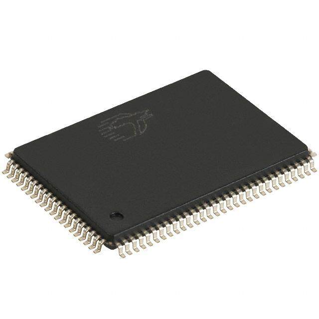
| 供应商器件封装 | 8-TSSOP |
| 其它名称 | 497-6347-6 |
| 其它有关文件 | http://www.st.com/web/catalog/mmc/FM76/CL1276/SC112/PF136741?referrer=70071840 |
| 包装 | Digi-Reel® |
| 商标 | STMicroelectronics |
| 存储器类型 | EEPROM |
| 存储容量 | 256 kbit |
| 安装风格 | SMD/SMT |
| 封装 | Reel |
| 封装/外壳 | 8-TSSOP(0.173",4.40mm 宽) |
| 封装/箱体 | TSSOP-8 |
| 工作温度 | -40°C ~ 85°C |
| 工作电流 | 2.5 mA |
| 工作电源电压 | 2.5 V, 3.3 V, 5 V |
| 工厂包装数量 | 4000 |
| 接口 | I²C,2 线串口 |
| 接口类型 | I2C |
| 数据保留 | 40 yr |
| 最大工作温度 | + 85 C |
| 最大工作电流 | 0.5 mA |
| 最大时钟频率 | 0.4 MHz |
| 最小工作温度 | - 40 C |
| 标准包装 | 1 |
| 格式-存储器 | EEPROMs - 串行 |
| 电压-电源 | 1.8 V ~ 5.5 V |
| 电源电压-最大 | 5.5 V |
| 电源电压-最小 | 1.8 V |
| 系列 | M24256-BR |
| 组织 | 32 k x 8 |
| 访问时间 | 900 ns |
| 速度 | 1MHz |


- 商务部:美国ITC正式对集成电路等产品启动337调查
- 曝三星4nm工艺存在良率问题 高通将骁龙8 Gen1或转产台积电
- 太阳诱电将投资9.5亿元在常州建新厂生产MLCC 预计2023年完工
- 英特尔发布欧洲新工厂建设计划 深化IDM 2.0 战略
- 台积电先进制程称霸业界 有大客户加持明年业绩稳了
- 达到5530亿美元!SIA预计今年全球半导体销售额将创下新高
- 英特尔拟将自动驾驶子公司Mobileye上市 估值或超500亿美元
- 三星加码芯片和SET,合并消费电子和移动部门,撤换高东真等 CEO
- 三星电子宣布重大人事变动 还合并消费电子和移动部门
- 海关总署:前11个月进口集成电路产品价值2.52万亿元 增长14.8%


_renders/IS42S32800D-6BLI.jpg)
PDF Datasheet 数据手册内容提取
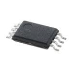
M24256-BW M24256-BR M24256-BF M24256-DR M24256-DF 256-Kbit serial I²C bus EEPROM Datasheet - production data Features • Compatible with all I2C bus modes: – 1 MHz – 400 kHz – 100 kHz • Memory array: TSSOP8 (DW) SO8 (MN) 169 mil width 150 mil width – 256 Kbit (32 Kbyte) of EEPROM – Page size: 64 byte – Additional Write lockable page (M24256-D order codes) • Single supply voltage and high speed: – 1 MHz clock from 1.7 V to 5.5 V UFDFPN8 (MC) • Write: DFN8 - 2x3 mm – Byte Write within 5 ms – Page Write within 5 ms • Operating temperature range: – from -40 °C up to +85 °C • Random and sequential Read modes • Write protect of the whole memory array WLCSP (CS) • Enhanced ESD/Latch-Up protection • More than 4 million Write cycles • More than 200-years data retention Packages • SO8 ECOPACK2® WLCSP (CU) • TSSOP8 ECOPACK2® • UFDFPN8 ECOPACK2® • WLCSP ECOPACK2® • Unsawn wafer (each die is tested) Unsawn wafer March 2018 DS1766 Rev 34 1/47 This is information on a product in full production. www.st.com
Contents M24256-BW M24256-BR M24256-BF M24256-DR M24256-DF Contents 1 Description . . . . . . . . . . . . . . . . . . . . . . . . . . . . . . . . . . . . . . . . . . . . . . . . . 6 2 Signal description . . . . . . . . . . . . . . . . . . . . . . . . . . . . . . . . . . . . . . . . . . . 8 2.1 Serial Clock (SCL) . . . . . . . . . . . . . . . . . . . . . . . . . . . . . . . . . . . . . . . . . . . 8 2.2 Serial Data (SDA) . . . . . . . . . . . . . . . . . . . . . . . . . . . . . . . . . . . . . . . . . . . . 8 2.3 Chip Enable (E2, E1, E0) . . . . . . . . . . . . . . . . . . . . . . . . . . . . . . . . . . . . . . 8 2.4 Write Control (WC) . . . . . . . . . . . . . . . . . . . . . . . . . . . . . . . . . . . . . . . . . . . 8 2.5 V (ground) . . . . . . . . . . . . . . . . . . . . . . . . . . . . . . . . . . . . . . . . . . . . . . . 8 SS 2.6 Supply voltage (V ) . . . . . . . . . . . . . . . . . . . . . . . . . . . . . . . . . . . . . . . . . 9 CC 2.6.1 Operating supply voltage (V ) . . . . . . . . . . . . . . . . . . . . . . . . . . . . . . . . 9 CC 2.6.2 Power-up conditions . . . . . . . . . . . . . . . . . . . . . . . . . . . . . . . . . . . . . . . . 9 2.6.3 Device reset . . . . . . . . . . . . . . . . . . . . . . . . . . . . . . . . . . . . . . . . . . . . . . . 9 2.6.4 Power-down conditions . . . . . . . . . . . . . . . . . . . . . . . . . . . . . . . . . . . . . . 9 3 Memory organization . . . . . . . . . . . . . . . . . . . . . . . . . . . . . . . . . . . . . . . 10 4 Device operation . . . . . . . . . . . . . . . . . . . . . . . . . . . . . . . . . . . . . . . . . . . 11 4.1 Start condition . . . . . . . . . . . . . . . . . . . . . . . . . . . . . . . . . . . . . . . . . . . . . . 12 4.2 Stop condition . . . . . . . . . . . . . . . . . . . . . . . . . . . . . . . . . . . . . . . . . . . . . . 12 4.3 Data input . . . . . . . . . . . . . . . . . . . . . . . . . . . . . . . . . . . . . . . . . . . . . . . . . 12 4.4 Acknowledge bit (ACK) . . . . . . . . . . . . . . . . . . . . . . . . . . . . . . . . . . . . . . 12 4.5 Device addressing . . . . . . . . . . . . . . . . . . . . . . . . . . . . . . . . . . . . . . . . . . 13 5 Instructions . . . . . . . . . . . . . . . . . . . . . . . . . . . . . . . . . . . . . . . . . . . . . . . 14 5.1 Write operations . . . . . . . . . . . . . . . . . . . . . . . . . . . . . . . . . . . . . . . . . . . . 14 5.1.1 Byte Write . . . . . . . . . . . . . . . . . . . . . . . . . . . . . . . . . . . . . . . . . . . . . . . 15 5.1.2 Page Write . . . . . . . . . . . . . . . . . . . . . . . . . . . . . . . . . . . . . . . . . . . . . . . 16 5.1.3 Write Identification Page (M24256-D only) . . . . . . . . . . . . . . . . . . . . . . 17 5.1.4 Lock Identification Page (M24256-D only) . . . . . . . . . . . . . . . . . . . . . . . 17 5.1.5 ECC (Error Correction Code) and Write cycling . . . . . . . . . . . . . . . . . . 17 5.1.6 Minimizing Write delays by polling on ACK . . . . . . . . . . . . . . . . . . . . . . 18 5.2 Read operations . . . . . . . . . . . . . . . . . . . . . . . . . . . . . . . . . . . . . . . . . . . . 19 5.2.1 Random Address Read . . . . . . . . . . . . . . . . . . . . . . . . . . . . . . . . . . . . . 20 2/47 DS1766 Rev 34
M24256-BW M24256-BR M24256-BF M24256-DR M24256-DF Contents 5.2.2 Current Address Read . . . . . . . . . . . . . . . . . . . . . . . . . . . . . . . . . . . . . . 20 5.2.3 Sequential Read . . . . . . . . . . . . . . . . . . . . . . . . . . . . . . . . . . . . . . . . . . 20 5.3 Read Identification Page (M24256-D only) . . . . . . . . . . . . . . . . . . . . . . . 20 5.4 Read the lock status (M24256-D only) . . . . . . . . . . . . . . . . . . . . . . . . . . . 21 6 Initial delivery state . . . . . . . . . . . . . . . . . . . . . . . . . . . . . . . . . . . . . . . . . 22 7 Maximum rating . . . . . . . . . . . . . . . . . . . . . . . . . . . . . . . . . . . . . . . . . . . . 23 8 DC and AC parameters . . . . . . . . . . . . . . . . . . . . . . . . . . . . . . . . . . . . . . 24 9 Package information . . . . . . . . . . . . . . . . . . . . . . . . . . . . . . . . . . . . . . . . 33 9.1 UFDFPN8 (DFN8) package information . . . . . . . . . . . . . . . . . . . . . . . . . . 33 9.2 TSSOP8 package information . . . . . . . . . . . . . . . . . . . . . . . . . . . . . . . . . 34 9.3 SO8N package information . . . . . . . . . . . . . . . . . . . . . . . . . . . . . . . . . . . 36 9.4 WLCSP8 (CS) package information . . . . . . . . . . . . . . . . . . . . . . . . . . . . . 38 9.5 WLCSP8 (CU) package information . . . . . . . . . . . . . . . . . . . . . . . . . . . . . 40 10 Ordering information . . . . . . . . . . . . . . . . . . . . . . . . . . . . . . . . . . . . . . . 42 11 Revision history . . . . . . . . . . . . . . . . . . . . . . . . . . . . . . . . . . . . . . . . . . . 45 DS1766 Rev 34 3/47 3
List of tables M24256-BW M24256-BR M24256-BF M24256-DR M24256-DF List of tables Table 1. Signal names . . . . . . . . . . . . . . . . . . . . . . . . . . . . . . . . . . . . . . . . . . . . . . . . . . . . . . . . . . . . 6 Table 2. Signals vs. bump position. . . . . . . . . . . . . . . . . . . . . . . . . . . . . . . . . . . . . . . . . . . . . . . . . . . 7 Table 3. Device select code . . . . . . . . . . . . . . . . . . . . . . . . . . . . . . . . . . . . . . . . . . . . . . . . . . . . . . . 13 Table 4. Most significant address byte. . . . . . . . . . . . . . . . . . . . . . . . . . . . . . . . . . . . . . . . . . . . . . . 14 Table 5. Least significant address byte . . . . . . . . . . . . . . . . . . . . . . . . . . . . . . . . . . . . . . . . . . . . . . 14 Table 6. Absolute maximum ratings. . . . . . . . . . . . . . . . . . . . . . . . . . . . . . . . . . . . . . . . . . . . . . . . . 23 Table 7. Operating conditions (voltage range W). . . . . . . . . . . . . . . . . . . . . . . . . . . . . . . . . . . . . . . 24 Table 8. Operating conditions (voltage range R) . . . . . . . . . . . . . . . . . . . . . . . . . . . . . . . . . . . . . . . 24 Table 9. Operating conditions (voltage range F) . . . . . . . . . . . . . . . . . . . . . . . . . . . . . . . . . . . . . . . 24 Table 10. AC measurement conditions. . . . . . . . . . . . . . . . . . . . . . . . . . . . . . . . . . . . . . . . . . . . . . . . 24 Table 11. Input parameters. . . . . . . . . . . . . . . . . . . . . . . . . . . . . . . . . . . . . . . . . . . . . . . . . . . . . . . . . 25 Table 12. Cycling performance by groups of four bytes. . . . . . . . . . . . . . . . . . . . . . . . . . . . . . . . . . . 25 Table 13. Memory cell data retention. . . . . . . . . . . . . . . . . . . . . . . . . . . . . . . . . . . . . . . . . . . . . . . . . 25 Table 14. DC characteristics (M24256-BW, device grade 6) . . . . . . . . . . . . . . . . . . . . . . . . . . . . . . . 26 Table 15. DC characteristics (M24256-BR, M24256-DR device grade 6) . . . . . . . . . . . . . . . . . . . . . 27 Table 16. DC characteristics (M24256-BF, M24256-DF, device grade 6) . . . . . . . . . . . . . . . . . . . . . 28 Table 17. 400 kHz AC characteristics. . . . . . . . . . . . . . . . . . . . . . . . . . . . . . . . . . . . . . . . . . . . . . . . . 29 Table 18. 1 MHz AC characteristics. . . . . . . . . . . . . . . . . . . . . . . . . . . . . . . . . . . . . . . . . . . . . . . . . . 30 Table 19. UFDFPN8 – 2x3 mm, 0.55 thickness, ultra thin fine pitch dual flat package, no lead - package mechanical data. . . . . . . . . . . . . . . . . . . . . . . . . . . . . . . . . . . . . . . . . . 33 Table 20. TSSOP8 – 3 x 4.4 mm, 0.65 mm pitch, 8-lead thin shrink small outline, package mechanical data. . . . . . . . . . . . . . . . . . . . . . . . . . . . . . . . . . . . . . . . . . . . . . . . . . 34 Table 21. SO8N – 3.9x4.9 mm, 8-lead plastic small outline, 150 mils body width, package mechanical data. . . . . . . . . . . . . . . . . . . . . . . . . . . . . . . . . . . . . . . . . . . . . . . . . . 36 Table 22. WLCSP (CS)- 8-bump, 1.289 x 1.376 mm, 0.4 mm pitch wafer level chip scale package mechanical data. . . . . . . . . . . . . . . . . . . . . . . . . . . . . . . . . . . . . . . . . . . . . . . . . . 38 Table 23. WLCSP (CU)- 8 balls, 1.289x1.1.309 mm, 0.4 mm pitch, with BSC, wafer level chip scale mechanical data . . . . . . . . . . . . . . . . . . . . . . . . . . . . . . . . . . . . . . . . . . . . . . . . 40 Table 24. Ordering information scheme. . . . . . . . . . . . . . . . . . . . . . . . . . . . . . . . . . . . . . . . . . . . . . . 42 Table 25. Ordering information scheme (unsawn wafer) . . . . . . . . . . . . . . . . . . . . . . . . . . . . . . . . . . 43 Table 26. Document revision history . . . . . . . . . . . . . . . . . . . . . . . . . . . . . . . . . . . . . . . . . . . . . . . . . 45 4/47 DS1766 Rev 34
M24256-BW M24256-BR M24256-BF M24256-DR M24256-DF List of figures List of figures Figure 1. Logic diagram. . . . . . . . . . . . . . . . . . . . . . . . . . . . . . . . . . . . . . . . . . . . . . . . . . . . . . . . . . . . 6 Figure 2. 8-pin package connections, top view . . . . . . . . . . . . . . . . . . . . . . . . . . . . . . . . . . . . . . . . . . 6 Figure 3. WLCSP connections. . . . . . . . . . . . . . . . . . . . . . . . . . . . . . . . . . . . . . . . . . . . . . . . . . . . . . . 7 Figure 4. Chip enable inputs connection . . . . . . . . . . . . . . . . . . . . . . . . . . . . . . . . . . . . . . . . . . . . . . . 8 Figure 5. Block diagram. . . . . . . . . . . . . . . . . . . . . . . . . . . . . . . . . . . . . . . . . . . . . . . . . . . . . . . . . . . 10 Figure 6. I2C bus protocol . . . . . . . . . . . . . . . . . . . . . . . . . . . . . . . . . . . . . . . . . . . . . . . . . . . . . . . . . 11 Figure 7. Write mode sequences with WC = 0 (data write enabled) . . . . . . . . . . . . . . . . . . . . . . . . . 15 Figure 8. Write mode sequences with WC = 1 (data write inhibited). . . . . . . . . . . . . . . . . . . . . . . . . 16 Figure 9. Write cycle polling flowchart using ACK. . . . . . . . . . . . . . . . . . . . . . . . . . . . . . . . . . . . . . . 18 Figure 10. Read mode sequences. . . . . . . . . . . . . . . . . . . . . . . . . . . . . . . . . . . . . . . . . . . . . . . . . . . . 19 Figure 11. AC measurement I/O waveform. . . . . . . . . . . . . . . . . . . . . . . . . . . . . . . . . . . . . . . . . . . . . 24 Figure 12. Maximum Rbus value versus bus parasitic capacitance (Cbus) for an I2C bus at maximum frequency fC = 400 kHz. . . . . . . . . . . . . . . . . . . . . . . . . . . . . . . . . . . . 31 Figure 13. Maximum R value versus bus parasitic capacitance C ) for bus bus an I2C bus at maximum frequency f = 1MHz . . . . . . . . . . . . . . . . . . . . . . . . . . . . . . . . . . 31 C Figure 14. AC waveforms . . . . . . . . . . . . . . . . . . . . . . . . . . . . . . . . . . . . . . . . . . . . . . . . . . . . . . . . . . 32 Figure 15. UFDFPN8 – 2x3 mm, 0.55 thickness, ultra thin fine pitch dual flat package, no lead - package outline . . . . . . . . . . . . . . . . . . . . . . . . . . . . . . . . . . . 33 Figure 16. TSSOP8 – 3x4.4 mm, 0.65 mm pitch, 8-lead thin shrink small outline, package outline. . . . . . . . . . . . . . . . . . . . . . . . . . . . . . . . . . . . . . . . . . . . . . . . . . . . . . . . . . 34 Figure 17. SO8N – 3.9x4.9 mm, 8-lead plastic small outline, 150 mils body width, package outline . 36 Figure 18. SO8N – 3.9x4.9 mm, 8-lead plastic small outline, 150 mils body width, package recommended footprint . . . . . . . . . . . . . . . . . . . . . . . . . . . . . . . . . . . . . . . . . . . . 37 Figure 19. WLCSP (CS) - 8-bump, 1.289 x 1.376 mm, 0.4 mm pitch wafer level chip scale package outline . . . . . . . . . . . . . . . . . . . . . . . . . . . . . . . . . . . . . . . . . . . . . . . . . . . . 38 Figure 20. WLCSP (CS) - 8-bump, 1.289 x 1.376 mm, 0.4 mm pitch wafer level chip scale package recommended footprint . . . . . . . . . . . . . . . . . . . . . . . . . . . . . . . . . . . . . . . 39 Figure 21. WLCSP (CU)- 8 balls, 1.289x1.1.309 mm, 0.4 mm pitch, with BSC, wafer level chip scale package outline . . . . . . . . . . . . . . . . . . . . . . . . . . . . . . . . . . . . . . . . . . . . 40 Figure 22. WLCSP (CU)- 8 balls, 1.289x1.1.309 mm, 0.4 mm pitch, with BSC, wafer level chip scale recommended footprint . . . . . . . . . . . . . . . . . . . . . . . . . . . . . . . . . . . . . . 41 DS1766 Rev 34 5/47 5
Description M24256-BW M24256-BR M24256-BF M24256-DR M24256-DF 1 Description The M24256 is a 256-Kbit I2C-compatible EEPROM (Electrically Erasable PROgrammable Memory) organized as 32 K × 8 bits. The M24256-BW can operate with a supply voltage from 2.5 V to 5.5 V, the M24256-BR and M24256-DR can operate with a supply voltage from 1.8 V to 5.5 V, and the M24256-BF and M24256-DF can operate with a supply voltage from 1.7 V to 5.5 V. All these devices operate with a clock frequency of 1 MHz (or less), over an ambient temperature range of –40 °C / +85 °C. The M24256-D offers an additional page, named the Identification Page (64 byte). The Identification Page can be used to store sensitive application parameters which can be (later) permanently locked in Read-only mode. Figure 1. Logic diagram (cid:57)(cid:38)(cid:38) (cid:22) (cid:40)(cid:19)(cid:16)(cid:40)(cid:21) (cid:54)(cid:39)(cid:36) (cid:48)(cid:21)(cid:23)(cid:91)(cid:91)(cid:91) (cid:54)(cid:38)(cid:47) (cid:58)(cid:38) (cid:57)(cid:54)(cid:54) (cid:36)(cid:44)(cid:19)(cid:20)(cid:27)(cid:23)(cid:23)(cid:73) Table 1. Signal names Signal name Function Direction E2, E1, E0 Chip Enable Input SDA Serial Data I/O SCL Serial Clock Input WC Write Control Input V Supply voltage - CC V Ground - SS Figure 2. 8-pin package connections, top view (cid:40)(cid:19) (cid:20) (cid:27) (cid:57)(cid:38)(cid:38) (cid:40)(cid:20) (cid:21) (cid:26) (cid:58)(cid:38) (cid:40)(cid:21) (cid:22) (cid:25) (cid:54)(cid:38)(cid:47) (cid:57)(cid:54)(cid:54) (cid:23) (cid:24) (cid:54)(cid:39)(cid:36) (cid:36)(cid:44)(cid:19)(cid:20)(cid:27)(cid:23)(cid:24)(cid:73) 1. See Section 9: Package information for package dimensions, and how to identify pin 1 6/47 DS1766 Rev 34
M24256-BW M24256-BR M24256-BF M24256-DR M24256-DF Description Figure 3. WLCSP connections (cid:20) (cid:21) (cid:22) (cid:22) (cid:21) (cid:20) (cid:36) (cid:116)(cid:18) (cid:28)(cid:1005) (cid:28)(cid:1005) (cid:116)(cid:18) (cid:36) (cid:37) (cid:28)(cid:1004) (cid:28)(cid:1004) (cid:37) (cid:38) (cid:115)(cid:18)(cid:18) (cid:115)(cid:94)(cid:94) (cid:115)(cid:94)(cid:94) (cid:115)(cid:18)(cid:18) (cid:38) (cid:39) (cid:94)(cid:24)(cid:4) (cid:94)(cid:24)(cid:4) (cid:39) (cid:40) (cid:94)(cid:18)(cid:62) (cid:28)(cid:1006) (cid:28)(cid:1006) (cid:94)(cid:18)(cid:62) (cid:40) (cid:48)(cid:68)(cid:85)(cid:78)(cid:76)(cid:81)(cid:74)(cid:3)(cid:86)(cid:76)(cid:71)(cid:72) (cid:37)(cid:88)(cid:80)(cid:83)(cid:3)(cid:86)(cid:76)(cid:71)(cid:72) (cid:11)(cid:87)(cid:82)(cid:83)(cid:3)(cid:89)(cid:76)(cid:72)(cid:90)(cid:12) (cid:11)(cid:69)(cid:82)(cid:87)(cid:87)(cid:82)(cid:80)(cid:3)(cid:89)(cid:76)(cid:72)(cid:90)(cid:12) (cid:48)(cid:54)(cid:22)(cid:19)(cid:28)(cid:20)(cid:28)(cid:57)(cid:23) Table 2. Signals vs. bump position Position A B C D E 1 WC - V - SCL CC 2 - E0 - SDA - 3 E1 - V - E2 SS DS1766 Rev 34 7/47 46
Signal description M24256-BW M24256-BR M24256-BF M24256-DR M24256-DF 2 Signal description 2.1 Serial Clock (SCL) The signal applied on the SCL input is used to strobe the data available on SDA(in) and to output the data on SDA(out). 2.2 Serial Data (SDA) SDA is an input/output used to transfer data in or data out of the device. SDA(out) is an open drain output that may be wire-OR’ed with other open drain or open collector signals on the bus. A pull-up resistor must be connected from Serial Data (SDA) to V (Figure 12 CC indicates how to calculate the value of the pull-up resistor). 2.3 Chip Enable (E2, E1, E0) (E2,E1,E0) input signals are used to set the value that is to be looked for on the three least significant bits (b3, b2, b1) of the 7-bit device select code (see Table 3). These inputs must be tied to V or V , as shown in Figure 4. When not connected (left floating), these inputs CC SS are read as low (0). Figure 4. Chip enable inputs connection (cid:57)(cid:38)(cid:38) (cid:57)(cid:38)(cid:38) (cid:48)(cid:21)(cid:23)(cid:91)(cid:91)(cid:91) (cid:48)(cid:21)(cid:23)(cid:91)(cid:91)(cid:91) (cid:40)(cid:76) (cid:40)(cid:76) (cid:57)(cid:54)(cid:54) (cid:57)(cid:54)(cid:54) (cid:36)(cid:76)(cid:20)(cid:21)(cid:27)(cid:19)(cid:25) 2.4 Write Control (WC) This input signal is useful for protecting the entire contents of the memory from inadvertent write operations. Write operations are disabled to the entire memory array when Write Control (WC) is driven high. Write operations are enabled when Write Control (WC) is either driven low or left floating. When Write Control (WC) is driven high, device select and address bytes are acknowledged, Data bytes are not acknowledged. 2.5 V (ground) SS V is the reference for the V supply voltage. SS CC 8/47 DS1766 Rev 34
M24256-BW M24256-BR M24256-BF M24256-DR M24256-DF Signal description 2.6 Supply voltage (V ) CC 2.6.1 Operating supply voltage (V ) CC Prior to selecting the memory and issuing instructions to it, a valid and stable V voltage CC within the specified [V (min), V (max)] range must be applied (see Operating conditions CC CC in Section 8: DC and AC parameters). In order to secure a stable DC supply voltage, it is recommended to decouple the V line with a suitable capacitor (usually of the order of CC 10 nF to 100 nF) close to the V /V package pins. CC SS This voltage must remain stable and valid until the end of the transmission of the instruction and, for a write instruction, until the completion of the internal write cycle (t ). W 2.6.2 Power-up conditions The V voltage has to rise continuously from 0 V up to the minimum V operating voltage CC CC (see Operating conditions in Section 8: DC and AC parameters). 2.6.3 Device reset In order to prevent inadvertent write operations during power-up, a power-on-reset (POR) circuit is included. At power-up, the device does not respond to any instruction until V has reached the CC internal reset threshold voltage. This threshold is lower than the minimum V operating CC voltage (see Operating conditions in Section 8: DC and AC parameters). When V passes CC over the POR threshold, the device is reset and enters the Standby Power mode; however, the device must not be accessed until V reaches a valid and stable DC voltage within the CC specified [V (min), V (max)] range (see Operating conditions in Section 8: DC and AC CC CC parameters). In a similar way, during power-down (continuous decrease in V ), the device must not be CC accessed when V drops below V (min). When V drops below the power-on-reset CC CC CC threshold voltage, the device stops responding to any instruction sent to it. 2.6.4 Power-down conditions During power-down (continuous decrease in V ), the device must be in the Standby Power CC mode (mode reached after decoding a Stop condition, assuming that there is no internal write cycle in progress). DS1766 Rev 34 9/47 46
Memory organization M24256-BW M24256-BR M24256-BF M24256-DR M24256-DF 3 Memory organization The memory is organized as shown below. Figure 5. Block diagram (cid:58)(cid:38) (cid:40)(cid:19) (cid:43)(cid:76)(cid:74)(cid:75)(cid:3)(cid:89)(cid:82)(cid:79)(cid:87)(cid:68)(cid:74)(cid:72) (cid:40)(cid:20) (cid:38)(cid:82)(cid:81)(cid:87)(cid:85)(cid:82)(cid:79)(cid:3)(cid:79)(cid:82)(cid:74)(cid:76)(cid:70) (cid:74)(cid:72)(cid:81)(cid:72)(cid:85)(cid:68)(cid:87)(cid:82)(cid:85) (cid:40)(cid:21) (cid:54)(cid:38)(cid:47) (cid:54)(cid:39)(cid:36) (cid:44)(cid:18)(cid:50)(cid:3)(cid:86)(cid:75)(cid:76)(cid:73)(cid:87)(cid:3)(cid:85)(cid:72)(cid:74)(cid:76)(cid:86)(cid:87)(cid:72)(cid:85) (cid:36)(cid:71)(cid:71)(cid:85)(cid:72)(cid:86)(cid:86)(cid:3)(cid:85)(cid:72)(cid:74)(cid:76)(cid:86)(cid:87)(cid:72)(cid:85) (cid:39)(cid:68)(cid:87)(cid:68) (cid:68)(cid:81)(cid:71)(cid:3)(cid:70)(cid:82)(cid:88)(cid:81)(cid:87)(cid:72)(cid:85) (cid:85)(cid:72)(cid:74)(cid:76)(cid:86)(cid:87)(cid:72)(cid:85) (cid:72)(cid:85) (cid:71) (cid:82) (cid:70) (cid:72) (cid:71) (cid:60)(cid:3) (cid:20)(cid:3)(cid:83)(cid:68)(cid:74)(cid:72) (cid:44)(cid:71)(cid:72)(cid:81)(cid:87)(cid:76)(cid:73)(cid:76)(cid:70)(cid:68)(cid:87)(cid:76)(cid:82)(cid:81)(cid:3)(cid:83)(cid:68)(cid:74)(cid:72) (cid:59)(cid:3)(cid:71)(cid:72)(cid:70)(cid:82)(cid:71)(cid:72)(cid:85) (cid:48)(cid:54)(cid:22)(cid:19)(cid:28)(cid:20)(cid:21)(cid:57)(cid:20) 10/47 DS1766 Rev 34
M24256-BW M24256-BR M24256-BF M24256-DR M24256-DF Device operation 4 Device operation The device supports the I2C protocol. This is summarized in Figure 6. Any device that sends data on to the bus is defined to be a transmitter, and any device that reads the data to be a receiver. The device that controls the data transfer is known as the bus master, and the other as the slave device. A data transfer can only be initiated by the bus master, which will also provide the serial clock for synchronization. The device is always a slave in all communications. Figure 6. I2C bus protocol (cid:54)(cid:38)(cid:47) (cid:54)(cid:39)(cid:36) (cid:54)(cid:39)(cid:36) (cid:54)(cid:39)(cid:36) (cid:54)(cid:55)(cid:36)(cid:53)(cid:55) (cid:44)(cid:81)(cid:83)(cid:88)(cid:87) (cid:38)(cid:75)(cid:68)(cid:81)(cid:74)(cid:72) (cid:54)(cid:55)(cid:50)(cid:51)(cid:3) (cid:38)(cid:82)(cid:81)(cid:71)(cid:76)(cid:87)(cid:76)(cid:82)(cid:81) (cid:38)(cid:82)(cid:81)(cid:71)(cid:76)(cid:87)(cid:76)(cid:82)(cid:81) (cid:54)(cid:38)(cid:47) (cid:20) (cid:21) (cid:22) (cid:26) (cid:27) (cid:28) (cid:54)(cid:39)(cid:36) (cid:48)(cid:54)(cid:37) (cid:36)(cid:38)(cid:46) (cid:54)(cid:55)(cid:36)(cid:53)(cid:55) (cid:38)(cid:82)(cid:81)(cid:71)(cid:76)(cid:87)(cid:76)(cid:82)(cid:81) (cid:54)(cid:38)(cid:47) (cid:20) (cid:21) (cid:22) (cid:26) (cid:27) (cid:28) (cid:54)(cid:39)(cid:36) (cid:48)(cid:54)(cid:37) (cid:36)(cid:38)(cid:46) (cid:94)(cid:100)(cid:75)(cid:87) (cid:3)(cid:18)(cid:381)(cid:374)(cid:282)(cid:349)(cid:410)(cid:349)(cid:381)(cid:374) (cid:48)(cid:54)(cid:24)(cid:19)(cid:19)(cid:20)(cid:21)(cid:57)(cid:20) DS1766 Rev 34 11/47 46
Device operation M24256-BW M24256-BR M24256-BF M24256-DR M24256-DF 4.1 Start condition Start is identified by a falling edge of Serial Data (SDA) while Serial Clock (SCL) is stable in the high state. A Start condition must precede any data transfer instruction. The device continuously monitors (except during a Write cycle) Serial Data (SDA) and Serial Clock (SCL) for a Start condition. 4.2 Stop condition Stop is identified by a rising edge of Serial Data (SDA) while Serial Clock (SCL) is stable and driven high. A Stop condition terminates communication between the device and the bus master. A Read instruction that is followed by NoAck can be followed by a Stop condition to force the device into the Standby mode. A Stop condition at the end of a Write instruction triggers the internal Write cycle. 4.3 Data input During data input, the device samples Serial Data (SDA) on the rising edge of Serial Clock (SCL). For correct device operation, Serial Data (SDA) must be stable during the rising edge of Serial Clock (SCL), and the Serial Data (SDA) signal must change only when Serial Clock (SCL) is driven low. 4.4 Acknowledge bit (ACK) The acknowledge bit is used to indicate a successful byte transfer. The bus transmitter, whether it be bus master or slave device, releases Serial Data (SDA) after sending eight bits of data. During the 9th clock pulse period, the receiver pulls Serial Data (SDA) low to acknowledge the receipt of the eight data bits. 12/47 DS1766 Rev 34
M24256-BW M24256-BR M24256-BF M24256-DR M24256-DF Device operation 4.5 Device addressing To start communication between the bus master and the slave device, the bus master must initiate a Start condition. Following this, the bus master sends the device select code, shown in Table 3 (most significant bit first). Table 3. Device select code Device type identifier(1) Chip Enable address(2) RW b7 b6 b5 b4 b3 b2 b1 b0 Device select code when addressing the 1 0 1 0 E2 E1 E0 RW memory array Device select code when accessing the 1 0 1 1 E2 E1 E0 RW Identification page 1. The most significant bit, b7, is sent first. 2. E0, E1 and E2 are compared with the value read on input pins E0, E1 and E2. When the device select code is received, the device only responds if the Chip Enable Address is the same as the value on the Chip Enable (E2, E1, E0) inputs. The 8th bit is the Read/Write bit (RW). This bit is set to 1 for Read and 0 for Write operations. If a match occurs on the device select code, the corresponding device gives an acknowledgment on Serial Data (SDA) during the 9th bit time. If the device does not match the device select code, it deselects itself from the bus, and goes into Standby mode. DS1766 Rev 34 13/47 46
Instructions M24256-BW M24256-BR M24256-BF M24256-DR M24256-DF 5 Instructions 5.1 Write operations Following a Start condition the bus master sends a device select code with the R/W bit (RW) reset to 0. The device acknowledges this, as shown in Figure 7, and waits for two address bytes. The device responds to each address byte with an acknowledge bit, and then waits for the data byte. Table 4. Most significant address byte A15 A14 A13 A12 A11 A10 A9 A8 Table 5. Least significant address byte A7 A6 A5 A4 A3 A2 A1 A0 When the bus master generates a Stop condition immediately after a data byte Ack bit (in the “10th bit” time slot), either at the end of a Byte Write or a Page Write, the internal Write cycle t is triggered. A Stop condition at any other time slot does not trigger the internal W Write cycle. After the Stop condition and the successful completion of an internal Write cycle (t ), the W device internal address counter is automatically incremented to point to the next byte after the last modified byte. During the internal Write cycle, Serial Data (SDA) is disabled internally, and the device does not respond to any requests. If the Write Control input (WC) is driven High, the Write instruction is not executed and the accompanying data bytes are not acknowledged, as shown in Figure 8. 14/47 DS1766 Rev 34
M24256-BW M24256-BR M24256-BF M24256-DR M24256-DF Instructions 5.1.1 Byte Write After the device select code and the address bytes, the bus master sends one data byte. If the addressed location is Write-protected, by Write Control (WC) being driven high, the device replies with NoAck, and the location is not modified. If, instead, the addressed location is not Write-protected, the device replies with Ack. The bus master terminates the transfer by generating a Stop condition, as shown in Figure 7. Figure 7. Write mode sequences with WC = 0 (data write enabled) (cid:58)(cid:38) (cid:36)(cid:38)(cid:46) (cid:36)(cid:38)(cid:46) (cid:36)(cid:38)(cid:46) (cid:36)(cid:38)(cid:46) (cid:37)(cid:92)(cid:87)(cid:72)(cid:3)(cid:58)(cid:85)(cid:76)(cid:87)(cid:72) (cid:39)(cid:72)(cid:89)(cid:3)(cid:86)(cid:72)(cid:79) (cid:37)(cid:92)(cid:87)(cid:72)(cid:3)(cid:68)(cid:71)(cid:71)(cid:85) (cid:37)(cid:92)(cid:87)(cid:72)(cid:3)(cid:68)(cid:71)(cid:71)(cid:85) (cid:39)(cid:68)(cid:87)(cid:68)(cid:3)(cid:76)(cid:81) (cid:68)(cid:85)(cid:87) (cid:54)(cid:87) (cid:53)(cid:18)(cid:58) (cid:58)(cid:38) (cid:36)(cid:38)(cid:46) (cid:36)(cid:38)(cid:46) (cid:36)(cid:38)(cid:46) (cid:36)(cid:38)(cid:46) (cid:51)(cid:68)(cid:74)(cid:72)(cid:3)(cid:58)(cid:85)(cid:76)(cid:87)(cid:72) (cid:39)(cid:72)(cid:89)(cid:3)(cid:86)(cid:72)(cid:79) (cid:37)(cid:92)(cid:87)(cid:72)(cid:3)(cid:68)(cid:71)(cid:71)(cid:85) (cid:37)(cid:92)(cid:87)(cid:72)(cid:3)(cid:68)(cid:71)(cid:71)(cid:85) (cid:39)(cid:68)(cid:87)(cid:68)(cid:3)(cid:76)(cid:81)(cid:3)(cid:20) (cid:39)(cid:68)(cid:87)(cid:68)(cid:3)(cid:76)(cid:81)(cid:3)(cid:21) (cid:68)(cid:85)(cid:87) (cid:54)(cid:87) (cid:53)(cid:18)(cid:58) (cid:58)(cid:38)(cid:3)(cid:11)(cid:70)(cid:82)(cid:81)(cid:87)(cid:182)(cid:71)(cid:12) (cid:36)(cid:38)(cid:46) (cid:36)(cid:38)(cid:46) (cid:51)(cid:68)(cid:74)(cid:72)(cid:3)(cid:58)(cid:85)(cid:76)(cid:87)(cid:72)(cid:3)(cid:11)(cid:70)(cid:82)(cid:81)(cid:87)(cid:182)(cid:71)(cid:12) (cid:39)(cid:68)(cid:87)(cid:68)(cid:3)(cid:76)(cid:81)(cid:3)(cid:49) (cid:83) (cid:82) (cid:54)(cid:87) (cid:36)(cid:44)(cid:19)(cid:20)(cid:20)(cid:19)(cid:25)(cid:71) DS1766 Rev 34 15/47 46
Instructions M24256-BW M24256-BR M24256-BF M24256-DR M24256-DF 5.1.2 Page Write The Page Write mode allows up to 64 byte to be written in a single Write cycle, provided that they are all located in the same page in the memory: that is, the most significant memory address bits, A15/A6, are the same. If more bytes are sent than will fit up to the end of the page, a “roll-over” occurs, i.e. the bytes exceeding the page end are written on the same page, from location 0. The bus master sends from 1 to 64 byte of data, each of which is acknowledged by the device if Write Control (WC) is low. If Write Control (WC) is high, the contents of the addressed memory location are not modified, and each data byte is followed by a NoAck, as shown in Figure 8. After each transferred byte, the internal page address counter is incremented. The transfer is terminated by the bus master generating a Stop condition. Figure 8. Write mode sequences with WC = 1 (data write inhibited) 16/47 DS1766 Rev 34
M24256-BW M24256-BR M24256-BF M24256-DR M24256-DF Instructions 5.1.3 Write Identification Page (M24256-D only) The Identification Page (64 byte) is an additional page which can be written and (later) permanently locked in Read-only mode. It is written by issuing the Write Identification Page instruction. This instruction uses the same protocol and format as Page Write (into memory array), except for the following differences: • Device type identifier = 1011b • MSB address bits A15/A6 are don't care except for address bit A10 which must be ‘0’. LSB address bits A5/A0 define the byte address inside the Identification page. If the Identification page is locked, the data bytes transferred during the Write Identification Page instruction are not acknowledged (NoAck). 5.1.4 Lock Identification Page (M24256-D only) The Lock Identification Page instruction (Lock ID) permanently locks the Identification page in Read-only mode. The Lock ID instruction is similar to Byte Write (into memory array) with the following specific conditions: • Device type identifier = 1011b • Address bit A10 must be ‘1’; all other address bits are don't care • The data byte must be equal to the binary value xxxx xx1x, where x is don't care 5.1.5 ECC (Error Correction Code) and Write cycling The Error Correction Code (ECC) is an internal logic function which is transparent for the I2C communication protocol. The ECC logic is implemented on each group of four EEPROM bytes(a). Inside a group, if a single bit out of the four bytes happens to be erroneous during a Read operation, the ECC detects this bit and replaces it with the correct value. The read reliability is therefore much improved. Even if the ECC function is performed on groups of four bytes, a single byte can be written/cycled independently. In this case, the ECC function also writes/cycles the three other bytes located in the same group(a). As a consequence, the maximum cycling budget is defined at group level and the cycling can be distributed over the 4 bytes of the group: the sum of the cycles seen by byte0, byte1, byte2 and byte3 of the same group must remain below the maximum value defined Table 11. a.A group of four bytes is located at addresses [4*N, 4*N+1, 4*N+2, 4*N+3], where N is an integer. DS1766 Rev 34 17/47 46
Instructions M24256-BW M24256-BR M24256-BF M24256-DR M24256-DF 5.1.6 Minimizing Write delays by polling on ACK The maximum Write time (t ) is shown in AC characteristics tables in Section 8: DC and AC w parameters, but the typical time is shorter. To make use of this, a polling sequence can be used by the bus master. The sequence, as shown in Figure 9, is: • Initial condition: a Write cycle is in progress. • Step 1: the bus master issues a Start condition followed by a device select code (the first byte of the new instruction). • Step 2: if the device is busy with the internal Write cycle, no Ack will be returned and the bus master goes back to Step 1. If the device has terminated the internal Write cycle, it responds with an Ack, indicating that the device is ready to receive the second part of the instruction (the first byte of this instruction having been sent during Step 1). Figure 9. Write cycle polling flowchart using ACK (cid:58)(cid:85)(cid:76)(cid:87)(cid:72)(cid:3)(cid:70)(cid:92)(cid:70)(cid:79)(cid:72) (cid:76)(cid:81)(cid:3)(cid:83)(cid:85)(cid:82)(cid:74)(cid:85)(cid:72)(cid:86)(cid:86)(cid:3)(cid:3) (cid:54)(cid:87)(cid:68)(cid:85)(cid:87)(cid:3)(cid:70)(cid:82)(cid:81)(cid:71)(cid:76)(cid:87)(cid:76)(cid:82)(cid:81) (cid:39)(cid:72)(cid:89)(cid:76)(cid:70)(cid:72)(cid:3)(cid:86)(cid:72)(cid:79)(cid:72)(cid:70)(cid:87) (cid:90)(cid:76)(cid:87)(cid:75)(cid:3)(cid:53)(cid:58)(cid:3)(cid:32)(cid:3)(cid:19) (cid:49)(cid:50) (cid:36)(cid:38)(cid:46) (cid:85)(cid:72)(cid:87)(cid:88)(cid:85)(cid:81)(cid:72)(cid:71) (cid:41)(cid:76)(cid:85)(cid:86)(cid:87)(cid:3)(cid:69)(cid:92)(cid:87)(cid:72)(cid:3)(cid:82)(cid:73)(cid:3)(cid:76)(cid:81)(cid:86)(cid:87)(cid:85)(cid:88)(cid:70)(cid:87)(cid:76)(cid:82)(cid:81)(cid:3) (cid:60)(cid:40)(cid:54) (cid:90)(cid:76)(cid:87)(cid:75)(cid:3)(cid:53)(cid:58)(cid:3)(cid:32)(cid:3)(cid:19)(cid:3)(cid:68)(cid:79)(cid:85)(cid:72)(cid:68)(cid:71)(cid:92)(cid:3) (cid:71)(cid:72)(cid:70)(cid:82)(cid:71)(cid:72)(cid:71)(cid:3)(cid:69)(cid:92)(cid:3)(cid:87)(cid:75)(cid:72)(cid:3)(cid:71)(cid:72)(cid:89)(cid:76)(cid:70)(cid:72) (cid:49)(cid:72)(cid:91)(cid:87) (cid:49)(cid:50) (cid:50)(cid:83)(cid:72)(cid:85)(cid:68)(cid:87)(cid:76)(cid:82)(cid:81)(cid:3)(cid:76)(cid:86) (cid:60)(cid:40)(cid:54) (cid:68)(cid:71)(cid:71)(cid:85)(cid:72)(cid:86)(cid:86)(cid:76)(cid:81)(cid:74)(cid:3)(cid:87)(cid:75)(cid:72) (cid:80)(cid:72)(cid:80)(cid:82)(cid:85)(cid:92) (cid:54)(cid:72)(cid:81)(cid:71)(cid:3)(cid:36)(cid:71)(cid:71)(cid:85)(cid:72)(cid:86)(cid:86) (cid:68)(cid:81)(cid:71)(cid:3)(cid:53)(cid:72)(cid:70)(cid:72)(cid:76)(cid:89)(cid:72)(cid:3)(cid:36)(cid:38)(cid:46) (cid:53)(cid:72)(cid:54)(cid:87)(cid:68)(cid:85)(cid:87) (cid:54)(cid:87)(cid:82)(cid:83) (cid:49)(cid:50) (cid:60)(cid:40)(cid:54) (cid:54)(cid:87)(cid:68)(cid:85)(cid:87)(cid:38)(cid:82)(cid:81)(cid:71)(cid:76)(cid:87)(cid:76)(cid:82)(cid:81) (cid:39)(cid:68)(cid:87)(cid:68)(cid:3)(cid:73)(cid:82)(cid:85)(cid:3)(cid:87)(cid:75)(cid:72) (cid:39)(cid:72)(cid:89)(cid:76)(cid:70)(cid:72)(cid:3)(cid:86)(cid:72)(cid:79)(cid:72)(cid:70)(cid:87) (cid:58)(cid:85)(cid:76)(cid:87)(cid:72)(cid:3)(cid:82)(cid:83)(cid:72)(cid:85)(cid:68)(cid:87)(cid:76)(cid:82)(cid:81) (cid:90)(cid:76)(cid:87)(cid:75)(cid:3)(cid:53)(cid:58)(cid:3)(cid:32)(cid:3)(cid:20) (cid:38)(cid:82)(cid:81)(cid:87)(cid:76)(cid:81)(cid:88)(cid:72)(cid:3)(cid:87)(cid:75)(cid:72) (cid:38)(cid:82)(cid:81)(cid:87)(cid:76)(cid:81)(cid:88)(cid:72)(cid:3)(cid:87)(cid:75)(cid:72) (cid:58)(cid:85)(cid:76)(cid:87)(cid:72)(cid:3)(cid:82)(cid:83)(cid:72)(cid:85)(cid:68)(cid:87)(cid:76)(cid:82)(cid:81) (cid:53)(cid:68)(cid:81)(cid:71)(cid:82)(cid:80)(cid:3)(cid:53)(cid:72)(cid:68)(cid:71)(cid:3)(cid:82)(cid:83)(cid:72)(cid:85)(cid:68)(cid:87)(cid:76)(cid:82)(cid:81) (cid:36)(cid:44)(cid:19)(cid:20)(cid:27)(cid:23)(cid:26)(cid:72) 1. The seven most significant bits of the Device Select code of a Random Read (bottom right box in the figure) must be identical to the seven most significant bits of the Device Select code of the Write (polling instruction in the figure). 18/47 DS1766 Rev 34
M24256-BW M24256-BR M24256-BF M24256-DR M24256-DF Instructions 5.2 Read operations Read operations are performed independently of the state of the Write Control (WC) signal. After the successful completion of a Read operation, the device internal address counter is incremented by one, to point to the next byte address. For the Read instructions, after each byte read (data out), the device waits for an acknowledgment (data in) during the 9th bit time. If the bus master does not acknowledge during this 9th time, the device terminates the data transfer and switches to its Standby mode. Figure 10. Read mode sequences (cid:36)(cid:38)(cid:46) (cid:49)(cid:50)(cid:3)(cid:36)(cid:38)(cid:46) (cid:38)(cid:88)(cid:85)(cid:85)(cid:72)(cid:81)(cid:87) (cid:36)(cid:71)(cid:71)(cid:85)(cid:72)(cid:86)(cid:86) (cid:39)(cid:72)(cid:89)(cid:3)(cid:86)(cid:72)(cid:79) (cid:39)(cid:68)(cid:87)(cid:68)(cid:3)(cid:82)(cid:88)(cid:87) (cid:53)(cid:72)(cid:68)(cid:71) (cid:68)(cid:85)(cid:87) (cid:82)(cid:83) (cid:54)(cid:87) (cid:53)(cid:18)(cid:58) (cid:54)(cid:87) (cid:36)(cid:38)(cid:46) (cid:36)(cid:38)(cid:46) (cid:36)(cid:38)(cid:46) (cid:36)(cid:38)(cid:46) (cid:49)(cid:50)(cid:3)(cid:36)(cid:38)(cid:46) (cid:53)(cid:68)(cid:81)(cid:71)(cid:82)(cid:80) (cid:36)(cid:71)(cid:71)(cid:85)(cid:72)(cid:86)(cid:86) (cid:39)(cid:72)(cid:89)(cid:3)(cid:86)(cid:72)(cid:79)(cid:3)(cid:13) (cid:37)(cid:92)(cid:87)(cid:72)(cid:3)(cid:68)(cid:71)(cid:71)(cid:85) (cid:37)(cid:92)(cid:87)(cid:72)(cid:3)(cid:68)(cid:71)(cid:71)(cid:85) (cid:39)(cid:72)(cid:89)(cid:3)(cid:86)(cid:72)(cid:79)(cid:3)(cid:13) (cid:39)(cid:68)(cid:87)(cid:68)(cid:3)(cid:82)(cid:88)(cid:87) (cid:53)(cid:72)(cid:68)(cid:71) (cid:68)(cid:85)(cid:87) (cid:68)(cid:85)(cid:87) (cid:82)(cid:83) (cid:54)(cid:87) (cid:53)(cid:18)(cid:58) (cid:54)(cid:87) (cid:53)(cid:18)(cid:58) (cid:54)(cid:87) (cid:36)(cid:38)(cid:46) (cid:36)(cid:38)(cid:46) (cid:36)(cid:38)(cid:46) (cid:49)(cid:50)(cid:3)(cid:36)(cid:38)(cid:46) (cid:54)(cid:72)(cid:84)(cid:88)(cid:72)(cid:81)(cid:87)(cid:76)(cid:68)(cid:79) (cid:38)(cid:88)(cid:85)(cid:85)(cid:72)(cid:81)(cid:87) (cid:39)(cid:72)(cid:89)(cid:3)(cid:86)(cid:72)(cid:79) (cid:39)(cid:68)(cid:87)(cid:68)(cid:3)(cid:82)(cid:88)(cid:87)(cid:3)(cid:20) (cid:39)(cid:68)(cid:87)(cid:68)(cid:3)(cid:82)(cid:88)(cid:87)(cid:3)(cid:49) (cid:53)(cid:72)(cid:68)(cid:71) (cid:68)(cid:85)(cid:87) (cid:82)(cid:83) (cid:54)(cid:87) (cid:53)(cid:18)(cid:58) (cid:54)(cid:87) (cid:36)(cid:38)(cid:46) (cid:36)(cid:38)(cid:46) (cid:36)(cid:38)(cid:46) (cid:36)(cid:38)(cid:46) (cid:36)(cid:38)(cid:46) (cid:54)(cid:72)(cid:84)(cid:88)(cid:72)(cid:81)(cid:87)(cid:76)(cid:68)(cid:79) (cid:53)(cid:68)(cid:81)(cid:71)(cid:82)(cid:80) (cid:39)(cid:72)(cid:89)(cid:3)(cid:86)(cid:72)(cid:79)(cid:3)(cid:13) (cid:37)(cid:92)(cid:87)(cid:72)(cid:3)(cid:68)(cid:71)(cid:71)(cid:85) (cid:37)(cid:92)(cid:87)(cid:72)(cid:3)(cid:68)(cid:71)(cid:71)(cid:85) (cid:39)(cid:72)(cid:89)(cid:3)(cid:86)(cid:72)(cid:79)(cid:3)(cid:13) (cid:39)(cid:68)(cid:87)(cid:68)(cid:3)(cid:82)(cid:88)(cid:87)(cid:20) (cid:53)(cid:72)(cid:68)(cid:71) (cid:68)(cid:85)(cid:87) (cid:68)(cid:85)(cid:87) (cid:54)(cid:87) (cid:53)(cid:18)(cid:58) (cid:54)(cid:87) (cid:53)(cid:18)(cid:58) (cid:36)(cid:38)(cid:46) (cid:49)(cid:50)(cid:3)(cid:36)(cid:38)(cid:46) (cid:39)(cid:68)(cid:87)(cid:68)(cid:3)(cid:82)(cid:88)(cid:87)(cid:3)(cid:49) (cid:83) (cid:82) (cid:54)(cid:87) (cid:36)(cid:44)(cid:19)(cid:20)(cid:20)(cid:19)(cid:24)(cid:71) DS1766 Rev 34 19/47 46
Instructions M24256-BW M24256-BR M24256-BF M24256-DR M24256-DF 5.2.1 Random Address Read A dummy Write is first performed to load the address into this address counter (as shown in Figure 10) but without sending a Stop condition. Then, the bus master sends another Start condition, and repeats the device select code, with the RW bit set to 1. The device acknowledges this, and outputs the contents of the addressed byte. The bus master must not acknowledge the byte, and terminates the transfer with a Stop condition. 5.2.2 Current Address Read For the Current Address Read operation, following a Start condition, the bus master only sends a device select code with the R/W bit set to 1. The device acknowledges this, and outputs the byte addressed by the internal address counter. The counter is then incremented. The bus master terminates the transfer with a Stop condition, as shown in Figure 10, without acknowledging the byte. Note that the address counter value is defined by instructions accessing either the memory or the Identification page. When accessing the Identification page, the address counter value is loaded with the byte location in the Identification page, therefore the next Current Address Read in the memory uses this new address counter value. When accessing the memory, it is safer to always use the Random Address Read instruction (this instruction loads the address counter with the byte location to read in the memory, see Section 5.2.1) instead of the Current Address Read instruction. 5.2.3 Sequential Read This operation can be used after a Current Address Read or a Random Address Read. The bus master does acknowledge the data byte output, and sends additional clock pulses so that the device continues to output the next byte in sequence. To terminate the stream of bytes, the bus master must not acknowledge the last byte, and must generate a Stop condition, as shown in Figure 10. The output data comes from consecutive addresses, with the internal address counter automatically incremented after each byte output. After the last memory address, the address counter “rolls-over”, and the device continues to output data from memory address 00h. 5.3 Read Identification Page (M24256-D only) The Identification Page (64 bytes) is an additional page which can be written and (later) permanently locked in Read-only mode. The Identification Page can be read by issuing an Read Identification Page instruction. This instruction uses the same protocol and format as the Random Address Read (from memory array) with device type identifier defined as 1011b. The MSB address bits A15/A6 are don't care, the LSB address bits A5/A0 define the byte address inside the Identification Page. The number of bytes to read in the ID page must not exceed the page boundary (e.g.: when reading the Identification Page from location 10d, the number of bytes should be less than or equal to 54, as the ID page boundary is 64 bytes). 20/47 DS1766 Rev 34
M24256-BW M24256-BR M24256-BF M24256-DR M24256-DF Instructions 5.4 Read the lock status (M24256-D only) The locked/unlocked status of the Identification page can be checked by transmitting a specific truncated command [Identification Page Write instruction + one data byte] to the device. The device returns an acknowledge bit if the Identification page is unlocked, otherwise a NoAck bit if the Identification page is locked. Right after this, it is recommended to transmit to the device a Start condition followed by a Stop condition, so that: • Start: the truncated command is not executed because the Start condition resets the device internal logic, • Stop: the device is then set back into Standby mode by the Stop condition. DS1766 Rev 34 21/47 46
Initial delivery state M24256-BW M24256-BR M24256-BF M24256-DR M24256-DF 6 Initial delivery state The device is delivered with all the memory array bits and Identification page bits set to 1 (each byte contains FFh). 22/47 DS1766 Rev 34
M24256-BW M24256-BR M24256-BF M24256-DR M24256-DF Maximum rating 7 Maximum rating Stressing the device outside the ratings listed in Table 6 may cause permanent damage to the device. These are stress ratings only, and operation of the device at these, or any other conditions outside those indicated in the operating sections of this specification, is not implied. Exposure to absolute maximum rating conditions for extended periods may affect device reliability. Table 6. Absolute maximum ratings Symbol Parameter Min. Max. Unit Ambient operating temperature -40 130 °C T Storage temperature –65 150 °C STG T Lead temperature during soldering see note (1) °C LEAD I DC output current (SDA = 0) - 5 mA OL V Input or output range –0.50 6.5 V IO V Supply voltage –0.50 6.5 V CC V Electrostatic pulse (Human Body model)(2) - 4000(3) V ESD 1. Compliant with JEDEC Std J-STD-020D (for small body, Sn-Pb or Pb-free assembly), the ST ECOPACK® 7191395 specification, and the European directive on Restrictions of Hazardous Substances (RoHS directive 2011/65/EU of July 2011). 2. Positive and negative pulses applied on different combinations of pin connections, according to AEC- Q100-002 (compliant with ANSI/ESDA/JEDEC JS-001-2012 standard, C1=100 pF, R1=1500 Ω). 3. 3000 V for previous devices (process letters KA). DS1766 Rev 34 23/47 46
DC and AC parameters M24256-BW M24256-BR M24256-BF M24256-DR M24256-DF 8 DC and AC parameters This section summarizes the operating and measurement conditions, and the DC and AC characteristics of the device. Table 7. Operating conditions (voltage range W) Symbol Parameter Min. Max. Unit V Supply voltage 2.5 5.5 V CC T Ambient operating temperature –40 85 °C A f Operating clock frequency - 1 MHz C Table 8. Operating conditions (voltage range R) Symbol Parameter Min. Max. Unit V Supply voltage 1.8 5.5 V CC T Ambient operating temperature –40 85 °C A f Operating clock frequency - 1 MHz C Table 9. Operating conditions (voltage range F) Symbol Parameter Min. Max. Unit V Supply voltage 1.7 5.5 V CC T Ambient operating temperature –40 85 °C A f Operating clock frequency - 1 MHz C Table 10. AC measurement conditions Symbol Parameter Min. Max. Unit C Load capacitance - 100 pF bus SCL input rise/fall time, SDA input fall time - 50 ns - Input levels 0.2 V to 0.8 V V - CC CC Input and output timing reference levels 0.3 V to 0.7 V V - CC CC Figure 11. AC measurement I/O waveform (cid:41)(cid:78)(cid:80)(cid:85)(cid:84)(cid:0)(cid:86)(cid:79)(cid:76)(cid:84)(cid:65)(cid:71)(cid:69)(cid:0)(cid:76)(cid:69)(cid:86)(cid:69)(cid:76)(cid:83) (cid:41)(cid:78)(cid:80)(cid:85)(cid:84)(cid:0)(cid:65)(cid:78)(cid:68)(cid:0)(cid:79)(cid:85)(cid:84)(cid:80)(cid:85)(cid:84) (cid:52)(cid:73)(cid:77)(cid:73)(cid:78)(cid:71)(cid:0)(cid:82)(cid:69)(cid:70)(cid:69)(cid:82)(cid:69)(cid:78)(cid:67)(cid:69)(cid:0)(cid:76)(cid:69)(cid:86)(cid:69)(cid:76)(cid:83) (cid:16)(cid:14)(cid:24)(cid:54)(cid:35)(cid:35) (cid:16)(cid:14)(cid:23)(cid:54)(cid:35)(cid:35) (cid:16)(cid:14)(cid:19)(cid:54)(cid:35)(cid:35) (cid:16)(cid:14)(cid:18)(cid:54)(cid:35)(cid:35) (cid:45)(cid:51)(cid:17)(cid:25)(cid:23)(cid:23)(cid:20)(cid:54)(cid:17) 24/47 DS1766 Rev 34
M24256-BW M24256-BR M24256-BF M24256-DR M24256-DF DC and AC parameters Table 11. Input parameters Symbol Parameter(1) Test condition Min. Max. Unit C Input capacitance (SDA) - - 8 pF IN C Input capacitance (other pins) - - 6 pF IN Z V < 0.3 V 30 - kΩ L Input impedance (E2, E1, E0, WC)(2) IN CC Z V > 0.7 V 500 - kΩ H IN CC 1. Characterized only, not tested in production. 2. E2, E1, E0 input impedance when the memory is selected (after a Start condition). Table 12. Cycling performance by groups of four bytes Symbol Parameter Test condition(1) Max. Unit Ncycle Write cycle TA ≤ 25 °C, VCC(min) < VCC < VCC(max) 4,000,000 Write cycle(3) endurance(2) T = 85 °C, V (min) < V < V (max) 1,200,000 A CC CC CC 1. Cycling performance for products identified by process letter K, previous devices were specified as 1 Million write cycle at 25°C. 2. The Write cycle endurance is defined for groups of four data bytes located at addresses [4*N, 4*N+1, 4*N+2, 4*N+3] where N is an integer. The Write cycle endurance is defined by characterization and qualification. 3. A Write cycle is executed when either a Page Write, a Byte Write, a Write Identification Page or a Lock Identification Page instruction is decoded. When using the Byte Write, the Page Write or the Write Identification Page, refer also to Section 5.1.5: ECC (Error Correction Code) and Write cycling. Table 13. Memory cell data retention Parameter Test condition Min. Unit Data retention(1) T = 55 °C 200 Year A 1. For products identified by process letter K. The data retention behavior is checked in production, while the 200-year limit is defined from characterization and qualification results. DS1766 Rev 34 25/47 46
DC and AC parameters M24256-BW M24256-BR M24256-BF M24256-DR M24256-DF Table 14. DC characteristics (M24256-BW, device grade 6) Test conditions (in addition to those Symbol Parameter Min. Max. Unit in Table 7) Input leakage current V = V orV , device in Standby I (SCL, SDA, E2, E1, IN SS CC - ± 2 µA LI mode E0) Output leakage SDA in Hi-Z, external voltage applied I - ± 2 µA LO current on SDA: V orV SS CC V = 2.5 V, f = 400 kHz CC c - 1 (rise/fall time < 50 ns) V = 5.5 V, f = 400 kHz I Supply current (Read) CC c - 2 mA CC (rise/fall time < 50 ns) 2.5 V ≤V ≤ 5.5 V, f = 1 MHz(1) CC c - 2.5 (rise/fall time < 50 ns) During t , I Supply current (Write) W - 2(2) mA CC0 2.5 V ≤ V ≤ 5.5 V CC Device not selected(3), - 2 µA Standby supply VIN = VSS or VCC, VCC = 2.5 V I CC1 current Device not selected(3), - 3 µA V = V orV , V = 5.5 V IN SS CC CC Input low voltage VIL (SCL, SDA, WC, E2, - –0.45 0.3 VCC V E1, E0)(4) Input high voltage - 0.7 V 6.5 V (SCL, SDA) CC V IH Input high voltage - 0.7 V V +0.6 V (WC, E2, E1, E0)(5) CC CC I = 2.1 mA, V = 2.5 V or V Output low voltage OL CC - 0.4 V OL I = 3 mA, V = 5.5 V OL CC 1. Only for devices operating at f max = 1 MHz (see Table 18). C 2. Characterized value, not tested in production. 3. The device is not selected after power-up, after a Read instruction (after the Stop condition), or after the completion of the internal write cycle t (t is triggered by the correct decoding of a Write instruction). W W 4. E inputs should be tied to V (see Section 2.3). i ss 5. E inputs should be tied to V (see Section 2.3). i cc 26/47 DS1766 Rev 34
M24256-BW M24256-BR M24256-BF M24256-DR M24256-DF DC and AC parameters Table 15. DC characteristics (M24256-BR, M24256-DR device grade 6) Test conditions(1) (in addition to Symbol Parameter Min. Max. Unit those in Table 8) Input leakage current V = V orV , device in I IN SS CC - ± 2 µA LI (E1, E2, SCL, SDA) Standby mode SDA in Hi-Z, external voltage I Output leakage current - ± 2 µA LO applied on SDA: V orV SS CC V = 1.8 V, f = 400 kHz - 0.8 mA CC c I Supply current (Read) CC f = 1 MHz(2) - 2.5 mA c I Supply current (Write) During tW - 2(3) mA CC0 V = 1.8 V ≤ V ≤ 2.5 V CC CC Device not selected(4), I Standby supply current - 1 µA CC1 V = V orV , V = 1.8 V IN SS CC CC Input low voltage V (SCL, SDA, WC, E2, 1.8 V ≤ V < 2.5 V –0.45 0.25 V V IL CC CC E1,E0)(5) Input high voltage 1.8 V ≤ V < 2.5 V 0.75 V 6.5 V (SCL, SDA) CC CC V IH Input high voltage 1.8 V ≤ V < 2.5 V 0.75 V V + 0.6 V (WC, E2, E1, E0)(6) CC CC CC V Output low voltage I = 1 mA, V = 1.8 V - 0.2 V OL OL CC 1. If the application uses the voltage range R device with 2.5 V < V < 5.5 V and -40 °C < T < +85 °C, cc A please refer to Table 14 instead of this table. 2. Only for devices identified with process letter K 3. Characterized value, not tested in production. 4. The device is not selected after power-up, after a Read instruction (after the Stop condition), or after the completion of the internal write cycle t (t is triggered by the correct decoding of a Write instruction). W W 5. E inputs should be tied to V (see Section 2.3). i ss 6. E inputs should be tied to V (see Section 2.3). i cc DS1766 Rev 34 27/47 46
DC and AC parameters M24256-BW M24256-BR M24256-BF M24256-DR M24256-DF Table 16. DC characteristics (M24256-BF, M24256-DF, device grade 6) Test conditions(1) (in addition to Symbol Parameter those in Table 9) Min. Max. Unit I Input leakage current VIN = VSS or VCC - ± 2 µA LI (E1, E2, SCL, SDA) device in Standby mode SDA in Hi-Z, external voltage applied I Output leakage current - ± 2 µA LO on SDA: V orV SS CC V = 1.7 V, f = 400 kHz - 0.8 CC C I Supply current (Read) mA CC f = 1 MHz(2) - 2.5 C I Supply current (Write) During t 1.7 V < V < 2.5 V - 2(3) mA CC0 W CC Device not selected(4), I Standby supply current - 1 µA CC1 V = V orV , V = 1.7 V IN SS CC CC Input low voltage V 1.7 V ≤ V < 2.5 V –0.45 0.25 V V IL (SCL, SDA, WC, E)(5) CC CC i Input high voltage 1.7 V ≤ V < 2.5 V 0.75 V 6.5 (SCL, SDA) CC CC V V IH Input high voltage 1.7 V ≤ V < 2.5 V 0.75 V V + 0.6 (WC, E2, E1, E0)(6) CC CC CC V Output low voltage I = 1 mA, V = 1.7 V - 0.2 V OL OL CC 1. If the application uses the voltage range F device with 2.5 V < V < 5.5 V and -40 °C < T < +85 °C, CC A please refer to Table 14 instead of this table. 2. Only for devices identified by process letter K (see Table 18). 3. Characterized value, not tested in production. 4. The device is not selected after power-up, after a Read instruction (after the Stop condition), or after the completion of the internal write cycle t (t is triggered by the correct decoding of a Write instruction). W W 5. Ei inputs should be tied to VSS(see Section 2.3). 6. Ei inputs should be tied to VCC (see Section 2.3). 28/47 DS1766 Rev 34
M24256-BW M24256-BR M24256-BF M24256-DR M24256-DF DC and AC parameters Table 17. 400 kHz AC characteristics Symbol Alt. Parameter Min. Max. Unit f f Clock frequency - 400 kHz C SCL t t Clock pulse width high 600 - ns CHCL HIGH t t Clock pulse width low 1300 - ns CLCH LOW t (1) t SDA (out) fall time 20(2) 300 ns QL1QL2 F t t Input signal rise time (3) (3) ns XH1XH2 R t t Input signal fall time (3) (3) ns XL1XL2 F t t Data in set up time 100 - ns DXCH SU:DAT t t Data in hold time 0 - ns CLDX HD:DAT t (4) t Data out hold time 100 - ns CLQX DH t (5) t Clock low to next data valid (access time) - 900 ns CLQV AA t t Start condition setup time 600 - ns CHDL SU:STA t t Start condition hold time 600 - ns DLCL HD:STA t t Stop condition set up time 600 - ns CHDH SU:STO Time between Stop condition and next Start t t 1300 - ns DHDL BUF condition t (6)(1) t WC set up time (before the Start condition) 0 - µs WLDL SU:WC t (7)(1) t WC hold time (after the Stop condition) 1 - µs DHWH HD:WC t t Internal Write cycle duration - 5 ms W WR Pulse width ignored (input filter on SCL and t (1) - - 80 ns NS SDA) - single glitch 1. Characterized only, not tested in production. 2. With C = 10 pF. L 3. There is no min. or max. values for the input signal rise and fall times. It is however recommended by the I²C specification that the input signal rise and fall times be more than 20 ns and less than 300 ns when f < 400 kHz. C 4. To avoid spurious Start and Stop conditions, a minimum delay is placed between SCL=1 and the falling or rising edge of SDA. 5. t is the time (from the falling edge of SCL) required by the SDA bus line to reach either 0.3V or CLQV CC 0.7V , assuming that R × C time constant is within the values specified in Figure 12. CC bus bus 6. WC=0 set up time condition to enable the execution of a WRITE command. 7. WC=0 hold time condition to enable the execution of a WRITE command. DS1766 Rev 34 29/47 46
DC and AC parameters M24256-BW M24256-BR M24256-BF M24256-DR M24256-DF Table 18. 1 MHz AC characteristics Symbol Alt. Parameter(1) Min. Max. Unit f f Clock frequency 0 1 MHz C SCL t t Clock pulse width high 260 - ns CHCL HIGH t t Clock pulse width low 500 - ns CLCH LOW t t Input signal rise time (2) (2) ns XH1XH2 R t t Input signal fall time (2) (2) ns XL1XL2 F t (3) t SDA (out) fall time 20(4) 120 ns QL1QL2 F t t Data in setup time 50 - ns DXCH SU:DAT t t Data in hold time 0 - ns CLDX HD:DAT t (5) t Data out hold time 100 - ns CLQX DH t (6) t Clock low to next data valid (access time) - 450(7) ns CLQV AA t t Start condition setup time 250 - ns CHDL SU:STA t t Start condition hold time 250 - ns DLCL HD:STA t t Stop condition setup time 250 - ns CHDH SU:STO Time between Stop condition and next Start t t 500 - ns DHDL BUF condition t (8)(3) t WC set up time (before the Start condition) 0 - µs WLDL SU:WC t (9)(3) t WC hold time (after the Stop condition) 1 - µs DHWH HD:WC t t Write time - 5 ms W WR Pulse width ignored (input filter on SCL and t (3) - - 50 ns NS SDA) 1. Only for devices identified by the process letter K (devices qualified at 1 MHz). 2. There is no min. or max. values for the input signal rise and fall times. It is however recommended by the I²C specification that the input signal rise and fall times be less than 120 ns when f < 1 MHz. C 3. Characterized only, not tested in production. 4. With C = 10 pF. L 5. To avoid spurious Start and Stop conditions, a minimum delay is placed between SCL=1 and the falling or rising edge of SDA. 6. t is the time (from the falling edge of SCL) required by the SDA bus line to reach either 0.3 V or CLQV CC 0.7 V , assuming that the Rbus × Cbus time constant is within the values specified in Figure 13. CC 7. 500 ns for the previous products. 8. WC=0 set up time condition to enable the execution of a WRITE command. 9. WC=0 hold time condition to enable the execution of a WRITE command. 30/47 DS1766 Rev 34
M24256-BW M24256-BR M24256-BF M24256-DR M24256-DF DC and AC parameters Figure 12. Maximum R value versus bus parasitic capacitance (C ) for bus bus an I2C bus at maximum frequency f = 400 kHz C (cid:79)(cid:82)(cid:0) (cid:17)(cid:16)(cid:16) (cid:83)(cid:84) (cid:83)(cid:73) (cid:34)(cid:85)(cid:83)(cid:0)(cid:76)(cid:73)(cid:78)(cid:69)(cid:0)(cid:80)(cid:85)(cid:76)(cid:76)(cid:13)(cid:85)(cid:80)(cid:0)(cid:82)(cid:69)(cid:8)(cid:75)(cid:9) (cid:17)(cid:20)(cid:0)(cid:75)(cid:16)(cid:189) (cid:40)(cid:69)(cid:82)(cid:69)(cid:0)(cid:50)(cid:66)(cid:85)(cid:83)(cid:0)(cid:167)(cid:0)(cid:35)(cid:66)(cid:85)(cid:83)(cid:0)(cid:29)(cid:0)(cid:17)(cid:18)(cid:16)(cid:50)(cid:0)(cid:66)(cid:78)(cid:85)(cid:83)(cid:83)(cid:0)(cid:167)(cid:0)(cid:35)(cid:66)(cid:85)(cid:83)(cid:0)(cid:29)(cid:0)(cid:20)(cid:16)(cid:16)(cid:0)(cid:78)(cid:83) (cid:52)(cid:77)(cid:84)(cid:79)(cid:73)(cid:77)(cid:78)(cid:72)(cid:85)(cid:0)(cid:69)(cid:69)(cid:83)(cid:84)(cid:72)(cid:0)(cid:84)(cid:0)(cid:50)(cid:0)(cid:67)(cid:69)(cid:66)(cid:79)(cid:0)(cid:0)(cid:66)(cid:69)(cid:0)(cid:76)(cid:78)(cid:0)(cid:69)(cid:85)(cid:0)(cid:0)(cid:83)(cid:83)(cid:66)(cid:0)(cid:70)(cid:0)(cid:84)(cid:84)(cid:69)(cid:88)(cid:14)(cid:65)(cid:0)(cid:76)(cid:78)(cid:79)(cid:35)(cid:84)(cid:87)(cid:0)(cid:66)(cid:0)(cid:0)(cid:76)(cid:85)(cid:0)(cid:0)(cid:73)(cid:78)(cid:84)(cid:0)(cid:83)(cid:72)(cid:0)(cid:0)(cid:69)(cid:84)(cid:69)(cid:73)(cid:77)(cid:0)(cid:82)(cid:0)(cid:20)(cid:69)(cid:69)(cid:0)(cid:16)(cid:80)(cid:0)(cid:67)(cid:16)(cid:82)(cid:69)(cid:79)(cid:0)(cid:78)(cid:83)(cid:78)(cid:83)(cid:69)(cid:83)(cid:78)(cid:84)(cid:65)(cid:84)(cid:69)(cid:78)(cid:68)(cid:84)(cid:41)(cid:163)(cid:35)(cid:0)(cid:66)(cid:85)(cid:83) (cid:51)(cid:35)(cid:44) (cid:54)(cid:35)(cid:35)(cid:50)(cid:66)(cid:85)(cid:83) (cid:45)(cid:18)(cid:20)(cid:88)(cid:88)(cid:88) (cid:77)(cid:65)(cid:83)(cid:84)(cid:69)(cid:82) (cid:17) (cid:51)(cid:36)(cid:33) (cid:19)(cid:16)(cid:0)(cid:80)(cid:38) (cid:17)(cid:16) (cid:17)(cid:16)(cid:16) (cid:17)(cid:16)(cid:16)(cid:16) (cid:35)(cid:66)(cid:85)(cid:83) (cid:34)(cid:85)(cid:83)(cid:0)(cid:76)(cid:73)(cid:78)(cid:69)(cid:0)(cid:67)(cid:65)(cid:80)(cid:65)(cid:67)(cid:73)(cid:84)(cid:79)(cid:82)(cid:0)(cid:8)(cid:80)(cid:38)(cid:9) (cid:65)(cid:73)(cid:17)(cid:20)(cid:23)(cid:25)(cid:22)(cid:66) Figure 13. Maximum R value versus bus parasitic capacitance C ) for bus bus an I2C bus at maximum frequency f = 1MHz C (cid:9)(cid:17)(cid:16)(cid:16) (cid:54)(cid:35)(cid:35) (cid:75) (cid:79)(cid:82)(cid:0)(cid:8) (cid:85)(cid:76)(cid:76)(cid:13)(cid:85)(cid:80)(cid:0)(cid:82)(cid:69)(cid:83)(cid:73)(cid:83)(cid:84) (cid:17)(cid:16) (cid:50)(cid:66)(cid:85)(cid:83)(cid:0)(cid:167)(cid:0)(cid:35)(cid:66)(cid:85)(cid:83)(cid:0)(cid:29)(cid:0)(cid:17)(cid:21)(cid:16)(cid:0)(cid:78)(cid:83) (cid:0) (cid:0) (cid:52)(cid:77)(cid:84)(cid:79)(cid:73)(cid:77)(cid:78)(cid:72)(cid:85)(cid:0)(cid:69)(cid:69)(cid:83)(cid:84)(cid:72)(cid:0)(cid:84)(cid:0)(cid:50)(cid:0)(cid:67)(cid:69)(cid:66)(cid:79)(cid:66)(cid:0)(cid:69)(cid:76)(cid:85)(cid:78)(cid:69)(cid:0)(cid:83)(cid:83)(cid:66)(cid:70)(cid:0)(cid:84)(cid:84)(cid:167)(cid:69)(cid:14)(cid:65)(cid:0)(cid:76)(cid:78)(cid:35)(cid:79)(cid:84)(cid:87)(cid:66)(cid:0)(cid:76)(cid:85)(cid:0)(cid:73)(cid:78)(cid:84)(cid:83)(cid:72)(cid:0)(cid:69)(cid:84)(cid:69)(cid:73)(cid:0)(cid:77)(cid:82)(cid:0)(cid:17)(cid:69)(cid:69)(cid:21)(cid:80)(cid:0)(cid:16)(cid:82)(cid:67)(cid:69)(cid:0)(cid:79)(cid:78)(cid:83)(cid:78)(cid:83)(cid:69)(cid:83)(cid:78)(cid:84)(cid:65)(cid:84)(cid:69)(cid:78)(cid:68)(cid:84) (cid:41)(cid:77)(cid:163)(cid:35)(cid:65)(cid:0)(cid:83)(cid:66)(cid:84)(cid:85)(cid:69)(cid:83)(cid:82) (cid:51)(cid:51)(cid:35)(cid:36)(cid:33)(cid:44) (cid:50)(cid:66)(cid:85)(cid:83) (cid:45)(cid:18)(cid:20)(cid:88)(cid:88)(cid:88) (cid:80) (cid:20) (cid:83)(cid:0)(cid:76)(cid:73)(cid:78)(cid:69)(cid:0) (cid:50)(cid:66)(cid:85)(cid:83)(cid:167)(cid:35)(cid:40)(cid:66)(cid:85)(cid:69)(cid:83)(cid:82)(cid:0)(cid:29)(cid:69)(cid:12)(cid:0)(cid:17)(cid:18)(cid:16)(cid:0)(cid:78)(cid:83) (cid:35)(cid:66)(cid:85)(cid:83) (cid:85) (cid:34) (cid:17) (cid:17)(cid:16) (cid:19)(cid:16) (cid:17)(cid:16)(cid:16) (cid:34)(cid:85)(cid:83)(cid:0)(cid:76)(cid:73)(cid:78)(cid:69)(cid:0)(cid:67)(cid:65)(cid:80)(cid:65)(cid:67)(cid:73)(cid:84)(cid:79)(cid:82)(cid:0)(cid:8)(cid:80)(cid:38)(cid:9) (cid:45)(cid:51)(cid:17)(cid:25)(cid:23)(cid:20)(cid:21)(cid:54)(cid:17) DS1766 Rev 34 31/47 46
DC and AC parameters M24256-BW M24256-BR M24256-BF M24256-DR M24256-DF Figure 14. AC waveforms (cid:94)(cid:410)(cid:258)(cid:396)(cid:410) (cid:94)(cid:410)(cid:381)(cid:393) (cid:94)(cid:410)(cid:258)(cid:396)(cid:410) (cid:272)(cid:381)(cid:374)(cid:282)(cid:349)(cid:410)(cid:349)(cid:381)(cid:374) (cid:272)(cid:381)(cid:374)(cid:282)(cid:349)(cid:410)(cid:349)(cid:381)(cid:374) (cid:272)(cid:381)(cid:374)(cid:282)(cid:349)(cid:410)(cid:349)(cid:381)(cid:374) (cid:410)(cid:121)(cid:62)(cid:1005)(cid:121)(cid:62)(cid:1006) (cid:410)(cid:18)(cid:44)(cid:18)(cid:62) (cid:410)(cid:121)(cid:44)(cid:1005)(cid:121)(cid:44)(cid:1006) (cid:410)(cid:18)(cid:62)(cid:18)(cid:44) (cid:94)(cid:18)(cid:62) (cid:410)(cid:24)(cid:62)(cid:18)(cid:62) (cid:410)(cid:121)(cid:62)(cid:1005)(cid:121)(cid:62)(cid:1006) (cid:94)(cid:24)(cid:4)(cid:3)(cid:47)(cid:374) (cid:94)(cid:24)(cid:4) (cid:410)(cid:18)(cid:44)(cid:24)(cid:62) (cid:410)(cid:121)(cid:44)(cid:1005)(cid:121)(cid:44)(cid:1006) (cid:47)(cid:374)(cid:393)(cid:437)(cid:410) (cid:410)(cid:18)(cid:62)(cid:24)(cid:121) (cid:94)(cid:24)(cid:4) (cid:410)(cid:24)(cid:121)(cid:18)(cid:44) (cid:410)(cid:18)(cid:44)(cid:24)(cid:44) (cid:410)(cid:24)(cid:44)(cid:24)(cid:62) (cid:18)(cid:346)(cid:258)(cid:374)(cid:336)(cid:286) (cid:116)(cid:18) (cid:410)(cid:116)(cid:62)(cid:24)(cid:62) (cid:410)(cid:24)(cid:44)(cid:116)(cid:44) (cid:94)(cid:410)(cid:381)(cid:393) (cid:94)(cid:410)(cid:258)(cid:396)(cid:410) (cid:272)(cid:381)(cid:374)(cid:282)(cid:349)(cid:410)(cid:349)(cid:381)(cid:374) (cid:272)(cid:381)(cid:374)(cid:282)(cid:349)(cid:410)(cid:349)(cid:381)(cid:374) (cid:94)(cid:18)(cid:62) (cid:94)(cid:24)(cid:4)(cid:3)(cid:47)(cid:374) (cid:410)(cid:116) (cid:410)(cid:18)(cid:44)(cid:24)(cid:44) (cid:410)(cid:18)(cid:44)(cid:24)(cid:62) (cid:116)(cid:396)(cid:349)(cid:410)(cid:286)(cid:3)(cid:272)(cid:455)(cid:272)(cid:367)(cid:286) (cid:410)(cid:18)(cid:44)(cid:18)(cid:62) (cid:94)(cid:18)(cid:62) (cid:410)(cid:18)(cid:62)(cid:89)(cid:115) (cid:410)(cid:18)(cid:62)(cid:89)(cid:121) (cid:410)(cid:89)(cid:62)(cid:1005)(cid:89)(cid:62)(cid:1006) (cid:94)(cid:24)(cid:4)(cid:3)(cid:75)(cid:437)(cid:410) (cid:24)(cid:258)(cid:410)(cid:258)(cid:3)(cid:448)(cid:258)(cid:367)(cid:349)(cid:282) (cid:24)(cid:258)(cid:410)(cid:258)(cid:3)(cid:448)(cid:258)(cid:367)(cid:349)(cid:282) (cid:4)(cid:47)(cid:1004)(cid:1004)(cid:1011)(cid:1013)(cid:1009)(cid:349) 32/47 DS1766 Rev 34
M24256-BW M24256-BR M24256-BF M24256-DR M24256-DF Package information 9 Package information In order to meet environmental requirements, ST offers these devices in different grades of ECOPACK® packages, depending on their level of environmental compliance. ECOPACK® specifications, grade definitions and product status are available at: www.st.com. ECOPACK® is an ST trademark. 9.1 UFDFPN8 (DFN8) package information Figure 15. UFDFPN8 – 2x3 mm, 0.55 thickness, ultra thin fine pitch dual flat package, no lead - package outline (cid:24) (cid:51)(cid:76)(cid:81)(cid:3)(cid:6)(cid:20)(cid:3)(cid:44)(cid:39)(cid:3)(cid:80)(cid:68)(cid:85)(cid:78)(cid:76)(cid:81)(cid:74) (cid:286) (cid:271) (cid:62)(cid:1005) (cid:62)(cid:1007) (cid:87)(cid:349)(cid:374)(cid:3)(cid:1005) (cid:28) (cid:28)(cid:1006) (cid:60) (cid:62) (cid:4) (cid:24)(cid:1006) (cid:286)(cid:286)(cid:286) (cid:4)(cid:1005) (cid:61)(cid:58)(cid:66)(cid:48)(cid:40)(cid:72)(cid:57)(cid:23) 1. Drawing is not to scale. 2. The central pad (the area E2 by D2 in the above illustration) must be either connected to V or left floating SS (not connected) in the end application. T able 19. UFDFPN8 – 2x3 mm, 0.55 thickness, ultra thin fine pitch dual flat package, no lead - package mechanical data millimeters inches(1) Symbol Min Typ Max Min Typ Max A 0.450 0.550 0.600 0.0177 0.0217 0.0236 A1 0.000 0.020 0.050 0.0000 0.0008 0.0020 b 0.200 0.250 0.300 0.0079 0.0098 0.0118 D 1.900 2.000 2.100 0.0748 0.0787 0.0827 D2 1.200 - 1.600 0.0472 - 0.0630 E 2.900 3.000 3.100 0.1142 0.1181 0.1220 E2 1.200 - 1.600 0.0472 - 0.0630 e - 0.500 - - 0.0197 - K 0.300 - - 0.0118 - - DS1766 Rev 34 33/47 46
Package information M24256-BW M24256-BR M24256-BF M24256-DR M24256-DF Table 19. UFDFPN8 – 2x3 mm, 0.55 thickness, ultra thin fine pitch dual flat package, no lead - package mechanical data (continued) millimeters inches(1) Symbol Min Typ Max Min Typ Max L 0.300 - 0.500 0.0118 - 0.0197 L1 - - 0.150 - - 0.0059 L3 0.300 - - 0.0118 - - eee(2) 0.080 - - 0.0031 - - 1. Values in inches are converted from mm and rounded to four decimal digits. 2. Applied for exposed die paddle and terminals. Exclude embedding part of exposed die paddle from measuring. 9.2 TSSOP8 package information Figure 16.TSSOP8 – 3x4.4 mm, 0.65 mm pitch, 8-lead thin shrink small outline, package outline (cid:24) (cid:1012) (cid:1009) (cid:272) (cid:28)(cid:1005) (cid:28) (cid:1005) (cid:1008) (cid:626) (cid:4)(cid:1005) (cid:62) (cid:4) (cid:4)(cid:1006) (cid:18)(cid:87) (cid:62)(cid:1005) (cid:271) (cid:286) (cid:55)(cid:54)(cid:54)(cid:50)(cid:51)(cid:27)(cid:36)(cid:48)(cid:66)(cid:57)(cid:21) 1. Drawing is not to scale. Table 20. TSSOP8 – 3 x 4.4 mm, 0.65 mm pitch, 8-lead thin shrink small outline, package mechanical data millimeters inches(1) Symbol Min. Typ. Max. Min. Typ. Max. A - - 1.200 - - 0.0472 A1 0.050 - 0.150 0.0020 - 0.0059 A2 0.800 1.000 1.050 0.0315 0.0394 0.0413 b 0.190 - 0.300 0.0075 - 0.0118 c 0.090 - 0.200 0.0035 - 0.0079 34/47 DS1766 Rev 34
M24256-BW M24256-BR M24256-BF M24256-DR M24256-DF Package information Table 20. TSSOP8 – 3 x 4.4 mm, 0.65 mm pitch, 8-lead thin shrink small outline, package mechanical data (continued) millimeters inches(1) Symbol Min. Typ. Max. Min. Typ. Max. CP - - 0.100 - - 0.0039 D 2.900 3.000 3.100 0.1142 0.1181 0.1220 e - 0.650 - - 0.0256 - E 6.200 6.400 6.600 0.2441 0.2520 0.2598 E1 4.300 4.400 4.500 0.1693 0.1732 0.1772 L 0.450 0.600 0.750 0.0177 0.0236 0.0295 L1 - 1.000 - - 0.0394 - α 0° - 8° 0° - 8° 1. Values in inches are converted from mm and rounded to four decimal digits. DS1766 Rev 34 35/47 46
Package information M24256-BW M24256-BR M24256-BF M24256-DR M24256-DF 9.3 SO8N package information Figure 17. SO8N – 3.9x4.9 mm, 8-lead plastic small outline, 150 mils body width, package outline (cid:72)(cid:0)(cid:88)(cid:0)(cid:20)(cid:21)(cid:131) (cid:33)(cid:18) (cid:33) (cid:67) (cid:67)(cid:67)(cid:67) (cid:66) (cid:69) (cid:19)(cid:17)(cid:21)(cid:24)(cid:3)(cid:80)(cid:80) (cid:36) (cid:42)(cid:36)(cid:56)(cid:42)(cid:40)(cid:3)(cid:51)(cid:47)(cid:36)(cid:49)(cid:40) (cid:75) (cid:24) (cid:37)(cid:17) (cid:37) (cid:17) (cid:33)(cid:17) (cid:44) (cid:44)(cid:17) (cid:54)(cid:50)(cid:16)(cid:36)(cid:66)(cid:57)(cid:21) 1. Drawing is not to scale. Table 21. SO8N – 3.9x4.9 mm, 8-lead plastic small outline, 150 mils body width, package mechanical data millimeters inches(1) Symbol Min. Typ. Max. Min. Typ. Max. A - - 1.750 - - 0.0689 A1 0.100 - 0.250 0.0039 - 0.0098 A2 1.250 - - 0.0492 - - b 0.280 - 0.480 0.0110 - 0.0189 c 0.170 - 0.230 0.0067 - 0.0091 D 4.800 4.900 5.000 0.1890 0.1929 0.1969 E 5.800 6.000 6.200 0.2283 0.2362 0.2441 E1 3.800 3.900 4.000 0.1496 0.1535 0.1575 e - 1.270 - - 0.0500 - h 0.250 - 0.500 0.0098 - 0.0197 k 0° - 8° 0° - 8° L 0.400 - 1.270 0.0157 - 0.0500 L1 - 1.040 - - 0.0409 - ccc - - 0.100 - - 0.0039 1. Values in inches are converted from mm and rounded to four decimal digits. 36/47 DS1766 Rev 34
M24256-BW M24256-BR M24256-BF M24256-DR M24256-DF Package information Figure 18. SO8N – 3.9x4.9 mm, 8-lead plastic small outline, 150 mils body width, package recommended footprint (cid:19)(cid:17)(cid:25)(cid:3)(cid:11)(cid:91)(cid:27)(cid:12) (cid:28)(cid:26) (cid:22)(cid:17)(cid:25)(cid:17) (cid:20)(cid:17)(cid:21)(cid:26) (cid:50)(cid:26)(cid:66)(cid:54)(cid:50)(cid:27)(cid:49)(cid:66)(cid:41)(cid:51)(cid:66)(cid:57)(cid:20) 1. Dimensions are expressed in millimeters. DS1766 Rev 34 37/47 46
Package information M24256-BW M24256-BR M24256-BF M24256-DR M24256-DF 9.4 WLCSP8 (CS) package information Figure 19. WLCSP (CS) - 8-bump, 1.289 x 1.376 mm, 0.4 mm pitch wafer level chip scale package outline (cid:69)(cid:69)(cid:69) (cid:61) (cid:39) (cid:43) (cid:72)(cid:21) (cid:59) (cid:60) (cid:72) (cid:41) (cid:39)(cid:72)(cid:87)(cid:68)(cid:76)(cid:79)(cid:3)(cid:36) (cid:40) (cid:72)(cid:20) (cid:72)(cid:22) (cid:41) (cid:53)(cid:72)(cid:73)(cid:72)(cid:85)(cid:72)(cid:81)(cid:70)(cid:72) (cid:68)(cid:68)(cid:68) (cid:36) (cid:11)(cid:23)(cid:59)(cid:12) (cid:36)(cid:21) (cid:42) (cid:50)(cid:85)(cid:76)(cid:72)(cid:81)(cid:87)(cid:68)(cid:87)(cid:76)(cid:82)(cid:81) (cid:58)(cid:68)(cid:73)(cid:72)(cid:85)(cid:3)(cid:69)(cid:68)(cid:70)(cid:78)(cid:3)(cid:86)(cid:76)(cid:71)(cid:72) (cid:54)(cid:76)(cid:71)(cid:72)(cid:3)(cid:89)(cid:76)(cid:72)(cid:90) (cid:37)(cid:88)(cid:80)(cid:83)(cid:3)(cid:86)(cid:76)(cid:71)(cid:72) (cid:37)(cid:88)(cid:80)(cid:83) (cid:36)(cid:20) (cid:72)(cid:72)(cid:72)(cid:0)(cid:0)(cid:61) (cid:69) (cid:61) (cid:140)(cid:70)(cid:70)(cid:70)(cid:3)(cid:48) (cid:58) (cid:56)(cid:57) (cid:140)(cid:71)(cid:71)(cid:71)(cid:3)(cid:48) (cid:58) (cid:54)(cid:72)(cid:68)(cid:87)(cid:76)(cid:81)(cid:74)(cid:3)(cid:83)(cid:79)(cid:68)(cid:81)(cid:72) (cid:39)(cid:72)(cid:87)(cid:68)(cid:76)(cid:79)(cid:3)(cid:36) (cid:53)(cid:82)(cid:87)(cid:68)(cid:87)(cid:72)(cid:71)(cid:3)(cid:28)(cid:19)(cid:3)(cid:131) (cid:20)(cid:38)(cid:74)(cid:66)(cid:48)(cid:40)(cid:66)(cid:57)(cid:23) 1. Drawing is not to scale. T able 22. WLCSP (CS)- 8-bump, 1.289 x 1.376 mm, 0.4 mm pitch wafer level chip scale package mechanical data millimeters inches(1) Symbol Min Typ Max Min Typ Max A 0.500 0.540 0.580 0.0197 0.0213 0.0228 A1 - 0.190 - - 0.0075 - A2 - 0.350 - - 0.0138 - b(2) - 0.270 - - 0.0106 - D - 1.289 1.309 - 0.0507 0.0515 E - 1.376 1.396 - 0.0542 0.0550 e - 0.800 - - 0.0315 - e1 - 0.693 - - 0.0273 - e2 - 0.400 - - 0.0157 - e3 - 0.400 - - 0.0157 - F - 0.342 - - 0.0135 - 38/47 DS1766 Rev 34
M24256-BW M24256-BR M24256-BF M24256-DR M24256-DF Package information Table 22. WLCSP (CS)- 8-bump, 1.289 x 1.376 mm, 0.4 mm pitch wafer level chip scale package mechanical data (continued) millimeters inches(1) Symbol Min Typ Max Min Typ Max G - 0.245 - - 0.0096 - H - 0.245 - - 0.0096 - aaa - 0.110 - - 0.0043 - bbb - 0.110 - - 0.0043 - ccc - 0.110 - - 0.0043 - ddd - 0.060 - - 0.0024 - eee - 0.060 - - 0.0024 - 1. Values in inches are converted from mm and rounded to 4 decimal digits. 2. Dimension is measured at the maximum bump diameter parallel to primary datum Z. Figure 20. WLCSP (CS) - 8-bump, 1.289 x 1.376 mm, 0.4 mm pitch wafer level chip scale package recommended footprint (cid:19)(cid:17)(cid:23)(cid:19)(cid:19)(cid:3)(cid:80)(cid:80) (cid:19)(cid:17)(cid:27)(cid:19)(cid:19)(cid:3)(cid:80)(cid:80) (cid:19)(cid:17)(cid:25)(cid:28)(cid:22)(cid:3)(cid:80)(cid:80) (cid:19)(cid:17)(cid:23)(cid:19)(cid:19)(cid:3)(cid:80)(cid:80) (cid:27)(cid:3)(cid:69)(cid:88)(cid:80)(cid:83)(cid:86)(cid:3)(cid:91)(cid:3)(cid:154)(cid:3)(cid:19)(cid:17)(cid:21)(cid:26)(cid:19)(cid:3)(cid:80)(cid:80) (cid:20)(cid:38)(cid:74)(cid:66)(cid:41)(cid:51)(cid:66)(cid:57)(cid:20) 1. Dimensions are expressed in millimeters. DS1766 Rev 34 39/47 46
Package information M24256-BW M24256-BR M24256-BF M24256-DR M24256-DF 9.5 WLCSP8 (CU) package information Figure 21. WLCSP (CU)- 8 balls, 1.289x1.1.309 mm, 0.4 mm pitch, with BSC, wafer level chip scale package outline (cid:72)(cid:20) (cid:68)(cid:68)(cid:68) (cid:11)(cid:21)(cid:59)(cid:12) (cid:61) (cid:39) (cid:59) (cid:81) (cid:69)(cid:69)(cid:69) (cid:39)(cid:72)(cid:87)(cid:68)(cid:76)(cid:79)(cid:3)(cid:36) (cid:72) (cid:60) (cid:72)(cid:70)(cid:87)(cid:76)(cid:82) (cid:42) (cid:82)(cid:87) (cid:83)(cid:85) (cid:72)(cid:3) (cid:22) (cid:40) (cid:68)(cid:70)(cid:78)(cid:86)(cid:76)(cid:71) (cid:21) (cid:72)(cid:21) (cid:72)(cid:22) (cid:37) (cid:20) (cid:41) (cid:69) (cid:68)(cid:68)(cid:68) (cid:36)(cid:22) (cid:36)(cid:20) (cid:40) (cid:39) (cid:38) (cid:37) (cid:36) (cid:50)(cid:85)(cid:76)(cid:72)(cid:81)(cid:87)(cid:68)(cid:87)(cid:76)(cid:82)(cid:81)(cid:3)(cid:85)(cid:72)(cid:73)(cid:72)(cid:85)(cid:72)(cid:81)(cid:70)(cid:72) (cid:11)(cid:21)(cid:59)(cid:12) (cid:36) (cid:50)(cid:85)(cid:76)(cid:72)(cid:81)(cid:87)(cid:68)(cid:87)(cid:76)(cid:82)(cid:81)(cid:3)(cid:85)(cid:72)(cid:73)(cid:72)(cid:85)(cid:72)(cid:81)(cid:70)(cid:72) (cid:36)(cid:21) (cid:55)(cid:50)(cid:51)(cid:3)(cid:57)(cid:44)(cid:40)(cid:58) (cid:54)(cid:44)(cid:39)(cid:40)(cid:3)(cid:57)(cid:44)(cid:40)(cid:58) (cid:37)(cid:50)(cid:55)(cid:55)(cid:50)(cid:48)(cid:3)(cid:57)(cid:44)(cid:40)(cid:58) (cid:69)(cid:69)(cid:69)(cid:61) (cid:36)(cid:20) (cid:69) (cid:61) (cid:70)(cid:70)(cid:70)(cid:48) (cid:61)(cid:59)(cid:60) (cid:71)(cid:71)(cid:71)(cid:48)(cid:61) (cid:39)(cid:72)(cid:87)(cid:68)(cid:76)(cid:79)(cid:3)(cid:36) (cid:54)(cid:72)(cid:68)(cid:87)(cid:76)(cid:81)(cid:74)(cid:3)(cid:83)(cid:79)(cid:68)(cid:81)(cid:72) (cid:53)(cid:82)(cid:87)(cid:68)(cid:87)(cid:72)(cid:71)(cid:3)(cid:28)(cid:19) (cid:36)(cid:19)(cid:61)(cid:26)(cid:66)(cid:51)(cid:55)(cid:73)(cid:66)(cid:58)(cid:47)(cid:38)(cid:54)(cid:51)(cid:27)(cid:66)(cid:48)(cid:40)(cid:66)(cid:57)(cid:20) 1. Drawing is not to scale. 2. Dimension is measured at the maximum bump diameter parallel to primary datum Z. 3. Primary datum Z and seating plane are defined by the spherical crowns of the bump. 4. Bump position designation per JESD 95-1, SPP-010. T able 23. WLCSP (CU)- 8 balls, 1.289x1.1.309 mm, 0.4 mm pitch, with BSC, wafer level chip scale mechanical data millimeters inches(1) Symbol Min Typ Max Min Typ Max A 0.255 0.295 0.335 0.0100 0.0116 0.0132 A1 - 0.095 - - 0.0037 - A2 - 0.175 - - 0.0069 - A3 - 0.025 - - 0.0010 - b - 0.185 - - 0.0073 - D - 1.289 1.309 - 0.0507 0.0515 E - 1.376 1.396 - 0.0542 0.0550 e - 0.400 - - 0.0157 - e1 - 0.800 - - 0.0315 - e2 - 0.346 - - 0.0136 - e3 - 0.693 - - 0.0273 - F - 0.342 - - 0.0135 - 40/47 DS1766 Rev 34
M24256-BW M24256-BR M24256-BF M24256-DR M24256-DF Package information Table 23. WLCSP (CU)- 8 balls, 1.289x1.1.309 mm, 0.4 mm pitch, with BSC, wafer level chip scale mechanical data (continued) millimeters inches(1) Symbol Min Typ Max Min Typ Max G - 0.245 - - 0.0096 - aaa - 0.110 - - 0.0043 - bbb - 0.110 - - 0.0043 - ccc - 0.110 - - 0.0043 - ddd - 0.060 - - 0.0024 - eee - 0.060 - - 0.0024 - 1. Values in inches are converted from mm and rounded to the 4rd decimal place. Figure 22. WLCSP (CU)- 8 balls, 1.289x1.1.309 mm, 0.4 mm pitch, with BSC, wafer level chip scale recommended footprint (cid:19)(cid:17)(cid:27)(cid:19)(cid:19) (cid:19)(cid:17)(cid:23)(cid:19)(cid:19) (cid:19)(cid:17)(cid:22)(cid:23)(cid:25) (cid:19)(cid:17)(cid:25)(cid:28)(cid:22) (cid:27)(cid:3)(cid:69)(cid:88)(cid:80)(cid:83)(cid:86)(cid:3)(cid:91)(cid:3)(cid:3)(cid:3)(cid:3)(cid:3)(cid:19)(cid:17)(cid:20)(cid:27)(cid:24) (cid:36)(cid:19)(cid:61)(cid:26)(cid:66)(cid:51)(cid:55)(cid:73)(cid:66)(cid:58)(cid:47)(cid:38)(cid:54)(cid:51)(cid:27)(cid:66)(cid:41)(cid:51)(cid:66)(cid:57)(cid:20) 1. Dimensions are expressed in millimeters. DS1766 Rev 34 41/47 46
Ordering information M24256-BW M24256-BR M24256-BF M24256-DR M24256-DF 10 Ordering information Table 24. Ordering information scheme Example: M24256-D W MN 6 T P /K Device type M24 = I2C serial access EEPROM Device function 256 = 256 Kbit (32 K x 8 bit) Device family B = Without Identification page D = With additional Identification page Operating voltage W = V = 2.5 V to 5.5 V CC R = V = 1.8 V to 5.5 V CC F = V = 1.7 V to 5.5 V CC Package(1) MN = SO8 (150 mil width) DW = TSSOP8 (169 mil width) MC = UFDFPN8 (DFN8) CS = WLCSP CU = WLCSP Ultra-Thin Device grade 6 = Industrial: device tested with standard test flow over -40 to 85 °C Option T = Tape and reel packing blank = tube packing Plating technology P or G = ECOPACK2® Process(2) /K = Manufacturing technology code 1. RoHS-compliant and halogen-free (ECOPACK2®) 2. The process letters apply to WLCSP device only. These process letters appear on the device package (marking) and on the shipment box. Please contact your nearest ST Sales Office for further information. 42/47 DS1766 Rev 34
M24256-BW M24256-BR M24256-BF M24256-DR M24256-DF Ordering information Table 25. Ordering information scheme (unsawn wafer)(1) Example: M24256 - B F K W 20 I / 90 Device type M24 = I2C serial access EEPROM Device function 256 = 256Kbit (32 K x 8 bit) Device family B = Without Identification page Operating voltage F = V = 1.7 V to 5.5 V CC Process K = F8H Delivery form W = Unsawn wafer Wafer thickness 20 = Non-backlapped wafer Wafer testing I = Inkless test Device grade 90 = -40°C to 85°C 1. For all information concerning the M24256 delivered in unsawn wafer, please contact your nearest ST Sales Office. DS1766 Rev 34 43/47 46
Ordering information M24256-BW M24256-BR M24256-BF M24256-DR M24256-DF Engineering samples Parts marked as ES or E are not yet qualified and therefore not approved for use in production. ST is not responsible for any consequences deriving from such use. In no event, will ST be liable for the customer using of these engineering samples in production. ST’s quality department must be contacted prior to any decision to use these engineering samples to run qualification activity. 44/47 DS1766 Rev 34
M24256-BW M24256-BR M24256-BF M24256-DR M24256-DF Revision history 11 Revision history Table 26. Document revision history Date Revision Changes Datasheet revision 25 split into: – M24256-125 datasheet for automotive products (range 3), – M24256-BW M24256-BR M24256-BF M24256-DR M24256-DF (this datasheet) for standard products (range 6). Added: – Reference M24256-DF – Table 1: Signal names, Table 12: Memory cell data retention Updated: 22-Jun-2012 26 – Table 17: 400 kHz AC characteristics and Table 18: 1 MHz AC characteristics: added set up and hold timing conditiions on WC (t WLDL and t ) DHWH – Figure 18: M24256-DFCS6TP/K, WLCSP 8-bump wafer-level chip scale package outline and Table 21: M24256-DFCS6TP/K, WLCSP 8- bump wafer-level chip scale package mechanical data – Cycling and data retention limits Deleted: – UFDFPN8, package revision MB Updated Figure 3: WLCSP connections and Figure 18: M24256- 01-Aug-2012 27 DFCS6TP/K, WLCSP 8-bump wafer-level chip scale package outline. Changed title of Figure 3: WLCSP connections. 18-Sep-2012 28 Updated Section 5.2.2: Current Address Read. 20-Nov-2012 29 Corrected “Device family” data in Table 24: Ordering information scheme. Deleted note (3) under Table 3: Device select code. Modified I condition in Table 15: DC characteristics (M24256-BR, CCO M24256-DR device grade 6). 17-Dec-2012 30 Deleted incorrect table (Table 15. DC characteristics (M24256-R, device grade 6)). Updated package list in Table 24: Ordering information scheme. Updated Figure 3: WLCSP connections. 21-Feb-2014 31 Added notes 4. and 5. in Table 14 and notes 5. and 6. in Table 15 and Table 16 Updated – Figure 3, 17-Jun-2014 32 – note 1 on Table 12 – In Table 24 note 1 on Package and blank reference on Option. DS1766 Rev 34 45/47 46
Revision history M24256-BW M24256-BR M24256-BF M24256-DR M24256-DF Table 26. Document revision history (continued) Date Revision Changes Added: – Unsawn wafer reference on cover page and Table 25: Ordering information scheme (unsawn wafer) – Figure 20: WLCSP (CS) - 8-bump, 1.289 x 1.376 mm, 0.4 mm pitch wafer level chip scale package recommended footprint – reference to Engineering samples Updated: 01-Jun-2015 33 – Section 2.6.2, Section 4.5 – Note 2 on Table 6 – Table 18 – Note 2 on Figure 15 – Table 21 – Note 2 on Table 24 Removed: – Note on t max value on Table 18 NS Added WLCSP (CU) package in cover page and in Section 9: Package information, Table 2: Signals vs. bump position. 14-Mar-2018 34 Updated Table 10: AC measurement conditions, Table 22: WLCSP (CS)- 8-bump, 1.289 x 1.376 mm, 0.4 mm pitch wafer level chip scale package mechanical data, Table 24: Ordering information scheme 46/47 DS1766 Rev 34
M24256-BW M24256-BR M24256-BF M24256-DR M24256-DF IMPORTANT NOTICE – PLEASE READ CAREFULLY STMicroelectronics NV and its subsidiaries (“ST”) reserve the right to make changes, corrections, enhancements, modifications, and improvements to ST products and/or to this document at any time without notice. Purchasers should obtain the latest relevant information on ST products before placing orders. ST products are sold pursuant to ST’s terms and conditions of sale in place at the time of order acknowledgement. Purchasers are solely responsible for the choice, selection, and use of ST products and ST assumes no liability for application assistance or the design of Purchasers’ products. No license, express or implied, to any intellectual property right is granted by ST herein. Resale of ST products with provisions different from the information set forth herein shall void any warranty granted by ST for such product. ST and the ST logo are trademarks of ST. All other product or service names are the property of their respective owners. Information in this document supersedes and replaces information previously supplied in any prior versions of this document. © 2018 STMicroelectronics – All rights reserved DS1766 Rev 34 47/47 47