ICGOO在线商城 > 分立半导体产品 > 二极管 - 整流器 - 单 > M1MA141KT1G

 Datasheet下载
- 型号: M1MA141KT1G
- 制造商: ON Semiconductor
- 库位|库存: xxxx|xxxx
- 要求:
| 数量阶梯 | 香港交货 | 国内含税 |
| +xxxx | $xxxx | ¥xxxx |
查看当月历史价格
查看今年历史价格
M1MA141KT1G产品简介:
ICGOO电子元器件商城为您提供M1MA141KT1G由ON Semiconductor设计生产,在icgoo商城现货销售,并且可以通过原厂、代理商等渠道进行代购。 M1MA141KT1G价格参考。ON SemiconductorM1MA141KT1G封装/规格:二极管 - 整流器 - 单, 标准 表面贴装 二极管 40V 100mA(DC) SC-70-3(SOT323)。您可以下载M1MA141KT1G参考资料、Datasheet数据手册功能说明书,资料中有M1MA141KT1G 详细功能的应用电路图电压和使用方法及教程。
型号为M1MA141KT1G的二极管由ON Semiconductor生产,属于整流二极管类别。该器件主要应用于电源整流电路中,用于将交流电(AC)转换为直流电(DC)。其典型应用场景包括:

1. 电源适配器和充电器:用于小型电子设备(如手机、平板、笔记本电脑)的电源适配器中,进行交流输入的整流处理。
2. 开关电源(SMPS):在各类电子设备的开关电源中作为输入整流元件,提供高效、稳定的整流功能。
3. 工业控制设备:用于工业自动化设备、仪表和控制系统中,为内部电路提供直流供电。
4. 照明设备:如LED驱动电源中,用于整流和电压转换。
5. 消费类电子产品:如电视、音响、小家电等设备的电源部分。

该器件采用表面贴装封装(如SMA),具有体积小、安装方便、可靠性高等优点,适用于中低功率的整流应用。其额定电流和耐压参数适中,适合多种通用电源设计。
| 参数 | 数值 |
| 产品目录 | |
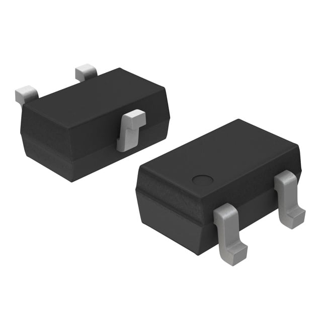
| 描述 | DIODE SWITCHING 40V 0.1A SC70-3二极管 - 通用,功率,开关 40V 100mA |
| 产品分类 | 单二极管/整流器分离式半导体 |
| 品牌 | ON Semiconductor |
| 产品手册 | |
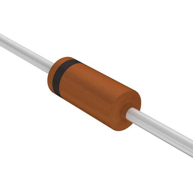
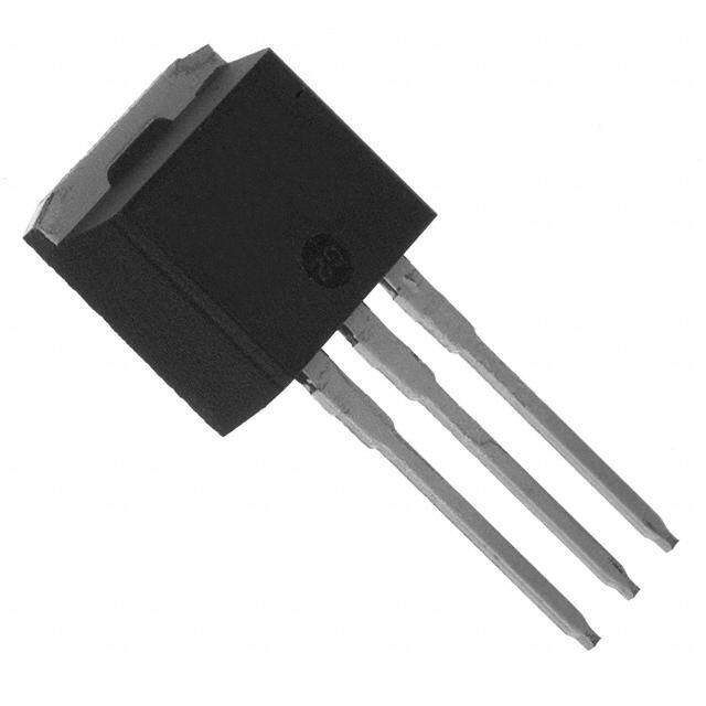
| 产品图片 |
|
| rohs | 符合RoHS无铅 / 符合限制有害物质指令(RoHS)规范要求 |
| 产品系列 | 二极管与整流器,二极管 - 通用,功率,开关,ON Semiconductor M1MA141KT1G- |
| 数据手册 | |
| 产品型号 | M1MA141KT1G |
| PCN设计/规格 | |
| 不同If时的电压-正向(Vf) | 1.2V @ 100mA |
| 不同 Vr、F时的电容 | 2pF @ 0V,1MHz |
| 不同 Vr时的电流-反向漏电流 | 100nA @ 35V |
| 二极管类型 | 标准 |
| 产品 | Switching Diodes |
| 产品目录页面 | |
| 产品种类 | 二极管 - 通用,功率,开关 |
| 供应商器件封装 | SC-70-3(SOT323) |
| 其它名称 | M1MA141KT1GOSDKR |
| 包装 | Digi-Reel® |
| 反向恢复时间(trr) | 3ns |
| 商标 | ON Semiconductor |
| 安装类型 | 表面贴装 |
| 安装风格 | SMD/SMT |
| 封装 | Reel |
| 封装/外壳 | SC-70,SOT-323 |
| 封装/箱体 | SC-70-6 |
| 峰值反向电压 | 40 V |
| 工作温度-结 | 150°C (最大) |
| 工作温度范围 | + 150 C |
| 工厂包装数量 | 3000 |
| 恢复时间 | 3 ns |
| 最大反向漏泄电流 | 0.1 uA |
| 最大工作温度 | + 150 C |
| 最大浪涌电流 | 0.5 A |
| 最小工作温度 | - 55 C |
| 标准包装 | 1 |
| 正向电压下降 | 1.2 V |
| 正向连续电流 | 0.225 A |
| 热阻 | - |
| 电压-DC反向(Vr)(最大值) | 40V |
| 电流-平均整流(Io) | 100mA(DC) |
| 系列 | M1MA141K |
| 速度 | 小信号 =< 200mA(Io),任意速度 |
| 配置 | Single |


- 商务部:美国ITC正式对集成电路等产品启动337调查
- 曝三星4nm工艺存在良率问题 高通将骁龙8 Gen1或转产台积电
- 太阳诱电将投资9.5亿元在常州建新厂生产MLCC 预计2023年完工
- 英特尔发布欧洲新工厂建设计划 深化IDM 2.0 战略
- 台积电先进制程称霸业界 有大客户加持明年业绩稳了
- 达到5530亿美元!SIA预计今年全球半导体销售额将创下新高
- 英特尔拟将自动驾驶子公司Mobileye上市 估值或超500亿美元
- 三星加码芯片和SET,合并消费电子和移动部门,撤换高东真等 CEO
- 三星电子宣布重大人事变动 还合并消费电子和移动部门
- 海关总署:前11个月进口集成电路产品价值2.52万亿元 增长14.8%


PDF Datasheet 数据手册内容提取
M1MA141KT1G, M1MA142KT1G Single Silicon Switching Diode ThisSiliconEpitaxialPlanarDiodeisdesignedforuseinultrahigh speed switching applications. This device is housed in the SC--70 http://onsemi.com packagewhichisdesignedforlowpowersurfacemountapplications. CATHODE Features 3 Fastt ,<3.0ns rr LowC ,<2.0pF D TheseDevicesarePb--Free,HalogenFree/BFRFreeandareRoHS Compliant ANODE NOCONNECTION MAXIMUMRATINGS(TA=25C) 1 2 Rating Symbol Value Unit ReverseVoltage VR Vdc 3 M1MA141KT1 40 SC--70(SOT--323) M1MA142KT1 80 CASE419 PeakReverseVoltage VRM Vdc 1 2 STYLE2 M1MA141KT1 40 M1MA142KT1 80 ForwardCurrent IF 100 mAdc MARKINGDIAGRAM PeakForwardCurrent IFM 225 mAdc PeakForwardSurgeCurrent IFSM 500 mAdc (Note1) MxMG G THERMALCHARACTERISTICS Rating Symbol Max Unit PowerDissipation PD 150 mW Mx =DeviceCode x= Hfor141 JunctionTemperature TJ 150 C Ifor142 M =DateCode* StorageTemperature Tstg --55~+150 C G =Pb--FreePackage Stresses exceeding Maximum Ratings may damage the device. Maximum (Note:Microdotmaybeineitherlocation) Ratingsarestressratingsonly.FunctionaloperationabovetheRecommended *Date Code orientation may vary depending upon OperatingConditionsisnotimplied.Extendedexposuretostressesabovethe manufacturinglocation. RecommendedOperatingConditionsmayaffectdevicereliability. 1. t=1sec ORDERINGINFORMATION Device Package Shipping† M1MA141KT1G SC--70 3000/Tape&Reel (Pb--Free) M1MA142KT1G SC--70 3000/Tape&Reel (Pb--Free) †Forinformationontapeandreelspecifications, includingpartorientationandtapesizes,please refertoourTapeandReelPackagingSpecifications Brochure,BRD8011/D. SemiconductorComponentsIndustries,LLC,2010 1 PublicationOrderNumber: October,2010--Rev.7 M1MA141KT1/D
M1MA141KT1G, M1MA142KT1G ELECTRICALCHARACTERISTICS(TA=25C) Characteristic Condition Symbol Min Max Unit ReverseVoltageLeakageCurrent IR -- 0.1 mAdc M1MA141KT1 VR=35V M1MA142KT1 VR=75V ForwardVoltage IF=100mA VF -- 1.2 Vdc ReverseBreakdownVoltage IR=100mA VR -- Vdc M1MA141KT1 40 M1MA142KT1 80 DiodeCapacitance VR=0,f=1.0MHz CD -- 2.0 pF ReverseRecoveryTime(Figure1) IF=10mA,VR=6.0V, trr -- 3.0 ns RL=100Ω,Irr=0.1IR (Note2) 2. trrTestCircuit http://onsemi.com 2
M1MA141KT1G, M1MA142KT1G RECOVERYTIMEEQUIVALENTTESTCIRCUIT INPUTPULSE OUTPUTPULSE tr tp trr IF t t 10% RL A Irr=0.1IR 90% IF=10mA VR tp=2ms VRRL==160V0Ω tr=0.35ns Figure1.RecoveryTimeEquivalentTestCircuit 100 10 TA=150C NT(mA) 10 TA=85C ENT(A) 1.0 TA=125C E R URR TA=--40C CUR TA=85C C E 0.1 D S R R ORWA 1.0 TA=25C REVE TA=55C F ,R0.01 ,F I I TA=25C 0.1 0.001 0.2 0.4 0.6 0.8 1.0 1.2 0 10 20 30 40 50 VF,FORWARDVOLTAGE(VOLTS) VR,REVERSEVOLTAGE(VOLTS) Figure2.ForwardVoltage Figure3.ReverseCurrent 0.68 F) (p 0.64 E C N A T CI PA 0.6 A C E D O DI ,D 0.56 C 0.52 0 2 4 6 8 VR,REVERSEVOLTAGE(VOLTS) Figure4.DiodeCapacitance http://onsemi.com 3
M1MA141KT1G, M1MA142KT1G PACKAGEDIMENSIONS SC--70(SOT--323) CASE419--04 ISSUEN D NOTES: 1. DIMENSIONINGANDTOLERANCINGPERANSIY14.5M,1982. e1 2. CONTROLLINGDIMENSION:INCH. MILLIMETERS INCHES 3 DIM MIN NOM MAX MIN NOM MAX A 0.80 0.90 1.00 0.032 0.035 0.040 HE E A1 0.00 0.05 0.10 0.000 0.002 0.004 1 2 A2 0.70REF 0.028REF b 0.30 0.35 0.40 0.012 0.014 0.016 c 0.10 0.18 0.25 0.004 0.007 0.010 D 1.80 2.10 2.20 0.071 0.083 0.087 b E 1.15 1.24 1.35 0.045 0.049 0.053 e 1.20 1.30 1.40 0.047 0.051 0.055 e e1 0.65BSC 0.026BSC L 0.20 0.38 0.56 0.008 0.015 0.022 HE 2.00 2.10 2.40 0.079 0.083 0.095 STYLE2: A A2 c PIN1.ANODE 2.N.C. 3.CATHODE 0.05(0.002) L A1 SOLDERINGFOOTPRINT* 0.65 0.65 0.025 0.025 1.9 0.075 0.9 0.035 0.7 0.028 SCALE10:1 mm inches *ForadditionalinformationonourPb--Freestrategyandsoldering details,pleasedownloadtheONSemiconductorSolderingand MountingTechniquesReferenceManual,SOLDERRM/D. ONSemiconductorand areregisteredtrademarksofSemiconductorComponentsIndustries,LLC(SCILLC).SCILLCreservestherighttomakechangeswithoutfurthernotice toanyproductsherein.SCILLCmakesnowarranty,representationorguaranteeregardingthesuitabilityofitsproductsforanyparticularpurpose,nordoesSCILLCassumeanyliability arisingoutoftheapplicationoruseofanyproductorcircuit,andspecificallydisclaimsanyandallliability,includingwithoutlimitationspecial,consequentialorincidentaldamages. “Typical”parameterswhichmaybeprovidedinSCILLCdatasheetsand/orspecificationscananddovaryindifferentapplicationsandactualperformancemayvaryovertime. All operatingparameters,including“Typicals”mustbevalidatedforeachcustomerapplicationbycustomer’stechnicalexperts. SCILLCdoesnotconveyanylicenseunderitspatent rightsnortherightsofothers. SCILLCproductsarenotdesigned,intended,orauthorizedforuseascomponentsinsystemsintendedforsurgicalimplantintothebody,orother applicationsintendedtosupportorsustainlife,orforanyotherapplicationinwhichthefailureoftheSCILLCproductcouldcreateasituationwherepersonalinjuryordeathmayoccur. ShouldBuyerpurchaseoruseSCILLCproductsforanysuchunintendedorunauthorizedapplication,BuyershallindemnifyandholdSCILLCanditsofficers,employees,subsidiaries, affiliates,anddistributorsharmlessagainstallclaims,costs,damages,andexpenses,andreasonableattorneyfeesarisingoutof,directlyorindirectly,anyclaimofpersonalinjury ordeathassociatedwithsuchunintendedorunauthorizeduse,evenifsuchclaimallegesthatSCILLCwasnegligentregardingthedesignormanufactureofthepart. SCILLCisan EqualOpportunity/AffirmativeActionEmployer. Thisliteratureissubjecttoallapplicablecopyrightlawsandisnotforresaleinanymanner. PUBLICATIONORDERINGINFORMATION LITERATUREFULFILLMENT: N.AmericanTechnicalSupport:800--282--9855TollFree ONSemiconductorWebsite:www.onsemi.com LiteratureDistributionCenterforONSemiconductor USA/Canada P.O.Box5163,Denver,Colorado80217USA Europe,MiddleEastandAfricaTechnicalSupport: OrderLiterature:http://www.onsemi.com/orderlit Phone:303--675--2175or800--344--3860TollFreeUSA/Canada Phone:421337902910 Fax:303--675--2176or800--344--3867TollFreeUSA/Canada JapanCustomerFocusCenter Foradditionalinformation,pleasecontactyourlocal Email:orderlit@onsemi.com Phone:81--3--5773--3850 SalesRepresentative http://onsemi.com M1MA141KT1/D 4