ICGOO在线商城 > 开发板,套件,编程器 > 评估和演示板和套件 > LV8736VGEVB

 Datasheet下载
- 型号: LV8736VGEVB
- 制造商: ON Semiconductor
- 库位|库存: xxxx|xxxx
- 要求:
| 数量阶梯 | 香港交货 | 国内含税 |
| +xxxx | $xxxx | ¥xxxx |
查看当月历史价格
查看今年历史价格
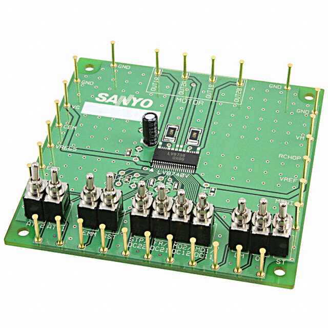
LV8736VGEVB产品简介:
ICGOO电子元器件商城为您提供LV8736VGEVB由ON Semiconductor设计生产,在icgoo商城现货销售,并且可以通过原厂、代理商等渠道进行代购。 LV8736VGEVB价格参考。ON SemiconductorLV8736VGEVB封装/规格:评估和演示板和套件, LV8736V 电机控制器/驱动器,步进 电源管理 Evaluation Board。您可以下载LV8736VGEVB参考资料、Datasheet数据手册功能说明书,资料中有LV8736VGEVB 详细功能的应用电路图电压和使用方法及教程。
ON Semiconductor(安森美)的LV8736VGEVB是一款针对LV8736VGG电机驱动器芯片设计的评估和演示板,主要用于评估该驱动器在步进电机控制中的性能。其典型应用场景包括消费类电子产品、办公自动化设备、工业控制系统以及小型家电中的精密电机驱动。

LV8736VGEVB支持微步进控制,可实现平滑、低噪音的电机运行,适用于对运动控制精度要求较高的场合,如打印机、扫描仪、摄像头云台、自动对焦机构和小型机器人等。通过该评估板,工程师可以快速验证LV8736VGG芯片的驱动能力、热性能和PWM控制特性,简化产品开发周期。

该评估板提供完整的外围电路和接口,支持与微控制器连接,便于调试和参数调整。同时具备过流、过热和欠压保护功能,确保测试过程安全可靠。LV8736VGEVB帮助用户深入了解芯片性能,加速从原型设计到量产的进程,特别适合需要高效、紧凑型步进电机驱动解决方案的研发项目。
| 参数 | 数值 |
| 产品目录 | 编程器,开发系统半导体 |
| 描述 | BOARD EVAL FOR LV8736V电源管理IC开发工具 EVM FOR LV8736V |
| 产品分类 | |
| 品牌 | ON Semiconductor |
| 产品手册 | |
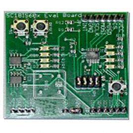
| 产品图片 |
|
| rohs | 符合RoHS无铅 / 符合限制有害物质指令(RoHS)规范要求 |
| 产品系列 | 电源管理IC开发工具,ON Semiconductor LV8736VGEVB- |
| 数据手册 | 点击此处下载产品Datasheethttp://www.onsemi.com/PowerSolutions/product.do?id=LV8736V&pdf=Y |
| 产品型号 | LV8736VGEVB |
| 主要属性 | - |
| 主要用途 | 电源管理,电机控制,步进控制器 |
| 产品 | Evaluation Boards |
| 产品培训模块 | http://www.digikey.cn/PTM/IndividualPTM.page?site=cn&lang=zhs&ptm=26221http://www.digikey.cn/PTM/IndividualPTM.page?site=cn&lang=zhs&ptm=26264 |
| 产品种类 | 电源管理IC开发工具 |
| 使用的IC/零件 | LV8736V |
| 其它名称 | LV8736VGEVBOS |
| 商标 | ON Semiconductor |
| 嵌入式 | - |
| 工具用于评估 | LV8736V |
| 所含物品 | 板 |
| 标准包装 | 1 |
| 类型 | Motor / Motion Controllers & Drivers |
| 设计资源 | 点击此处下载产品Datasheethttp://www.onsemi.com/pub/Collateral/LV8736VGEVB_GERBER.ZIP点击此处下载产品Datasheet点击此处下载产品Datasheet |
| 辅助属性 | - |


- 商务部:美国ITC正式对集成电路等产品启动337调查
- 曝三星4nm工艺存在良率问题 高通将骁龙8 Gen1或转产台积电
- 太阳诱电将投资9.5亿元在常州建新厂生产MLCC 预计2023年完工
- 英特尔发布欧洲新工厂建设计划 深化IDM 2.0 战略
- 台积电先进制程称霸业界 有大客户加持明年业绩稳了
- 达到5530亿美元!SIA预计今年全球半导体销售额将创下新高
- 英特尔拟将自动驾驶子公司Mobileye上市 估值或超500亿美元
- 三星加码芯片和SET,合并消费电子和移动部门,撤换高东真等 CEO
- 三星电子宣布重大人事变动 还合并消费电子和移动部门
- 海关总署:前11个月进口集成电路产品价值2.52万亿元 增长14.8%
PDF Datasheet 数据手册内容提取
Ordering number : ENA1785C LV8736V Monolithic Linear IC PWM Constant-Current Control http://onsemi.com Stepper Motor Driver Overview The LV8736V is a 2-channel H-bridge driver IC that can switch a stepper motor driver, which is capable of micro-step drive and supports 1/8 step excitation, and two channels of a brushed motor driver, which supports forward, reverse, brake, and standby of a motor. It is ideally suited for driving brushed DC motors and stepper motors used in office equipment and amusement applications. Function • Single-channel PWM current control stepper motor driver (selectable with DC motor driver channel 2) incorporated. • BiCDMOS process IC • Low on resistance (upper side : 0.75Ω ; lower side : 0.5Ω ; total of upper and lower : 1.25Ω ; Ta = 25°C, IO = 1A) • Excitation mode can be set to Full step, Half step, Quarter step , or 1/8 step • Excitation step proceeds only by step signal input • Motor current selectable in four steps • Output short-circuit protection circuit (selectable from latch-type or auto-reset-type) incorporated • Unusual condition warning output pins • Built-in thermal shutdown circuit • No control power supply required Specifications Absolute Maximum Ratings at Ta = 25°C Parameter Symbol Conditions Ratings Unit Supply voltage VM max VM , VM1 , VM2 36 V Output peak current IO peak tw ≤ 10ms , duty 20% Per 1ch 1.5 A Output current IO max Per 1ch 1 A Logic input voltage VIN max ST , DM , STEP/DC22 , FR/DC21 , -0.3 to +6 V MD2/DC12 , ATT1 , ATT2 , EMM , RST/BLK , OE/CMK MONI/EMO input voltage Vmo/Vemo -0.3 to +6 V Allowable power dissipation Pd max * 3.05 W Operating temperature Topr -40 to +85 °C Storage temperature Tstg -55 to +150 °C * Specified circuit board : 90.0mm×90.0mm×1.6mm, glass epoxy 2-layer board, with backside mounting. Caution 1) Absolute maximum ratings represent the value which cannot be exceeded for any length of time. Caution 2) Even when the device is used within the range of absolute maximum ratings, as a result of continuous usage under high temperature, high current, high voltage, or drastic temperature change, the reliability of the IC may be degraded. Please contact us for the further details. StressesexceedingMaximumRatingsmaydamagethedevice.MaximumRatingsarestressratingsonly.FunctionaloperationabovetheRecommendedOperating Conditions is not implied. Extended exposure to stresses above the Recommended Operating Conditions may affect device reliability. ORDERING INFORMATION See detailed ordering and shipping information on page 26 of this data sheet. Semiconductor Components Industries, LLC, 2013 June, 2013 61913NK / 42413NK 20130115-S00005 No.A1785-1/26
LV8736V Allowable Operating Ratings at Ta = 25°C Parameter Symbol Conditions Ratings Unit Supply voltage range VM VM, VM1, VM2 9 to 32 V Logic input voltage VIN ST, DM, STEP/DC22, FR/DC21, MD1/DC11, MD2/DC12, 0 to 5.5 V ATT1, ATT2, EMM, RST/BLK, OE/CMK VREF input voltage range VREF 0 to 3 V Electrical Characteristics at Ta = 25°C, VM = 24V, VREF = 1.5V Ratings Parameter Symbol Conditions Unit min typ max Standby mode current drain IMst ST = “L” , IM(VM)+IM1(VM1)+IM2(VM2) 100 400 μA Current drain IM ST = “H”, OE = “L”, with no load , 3.2 5 mA IM(VM)+IM1(VM1)+IM2(VM2) VREG5 output voltage Vreg5 IO = -1mA 4.5 5 5.5 V Thermal shutdown temperature TSD Design guarantee 150 180 200 °C Thermal hysteresis width ΔTSD Design guarantee 40 °C Motor driver Output on resistance Ronu IO = 1A, Upper-side on resistance 0.75 0.97 Ω Rond IO = 1A, Lower-side on resistance 0.5 0.65 Ω Output leakage current IOleak 50 μA Diode forward voltage VD ID = -1A 1.2 1.4 V Logic input voltage High VINh ST, DM, STEP/DC22, FR/DC21, MD1/DC11, 2.0 5.5 V Low VINl MD2/DC12, ATT1, ATT2, EMM, RST/BLK, 0 0.8 V OE/CMK Logic pin input current IINL ST, DM, STEP/DC22, FR/DC21, MD1/DC11, 4 8 12 μA other OE/CMK pin MD2/DC12, ATT1, ATT2, EMM, RST/BLK, VIN = 0.8V IINH VIN = 5V 30 50 70 μA OE / CMK pin input current ICMKL DM = “L”, OE/CMK = 0.8V 4 8 12 μA ICMKH DM = “L”, OE/CMK = 5V 30 50 70 μA ICMK DM = “H”, OE/CMK = 0V -32 -25 -18 μA OE/CMK pin current LIMIT mask VtCMK DM = “H” 1.2 1.5 1.8 V threshold voltage. Current setting 1/8 step drive Vtdac0_2W Step 0 (When initialized : channel 1 0.291 0.3 0.309 V comparator comparator level) threshold Vtdac1_2W Step 1 (Initial state+1) 0.285 0.294 0.303 V voltage Vtdac2_2W Step 2 (Initial state+2) 0.267 0.276 0.285 V (current step Vtdac3_2W Step 3 (Initial state+3) 0.240 0.249 0.258 V switching) Vtdac4_2W Step 4 (Initial state+4) 0.201 0.21 0.219 V Vtdac5_2W Step 5 (Initial state+5) 0.157 0.165 0.173 V Vtdac6_2W Step 6 (Initial state+6) 0.107 0.114 0.121 V Vtdac7_2W Step 7 (Initial state+7) 0.053 0.06 0.067 V Quarter step Vtdac0_W Step 0 (When initialized : channel 1 0.291 0.3 0.309 V drive comparator level) Vtdac2_W Step 2 (Initial state+1) 0.267 0.276 0.285 V Vtdac4_W Step 4 (Initial state+2) 0.201 0.21 0.219 V Vtdac6_W Step 6 (Initial state+3) 0.107 0.114 0.121 V Half step drive Vtdac0_H Step 0 (When initialized : channel 1 0.291 0.3 0.309 V comparator level) Vtdac4_H Step 4 (Initial state+1) 0.201 0.21 0.219 V Full step drive Vtdac4_F Step 4' (When initialized : channel 1 0.291 0.3 0.309 V comparator level) Current setting comparator Vtatt00 ATT1 = L, ATT2 = L 0.291 0.3 0.309 V threshold voltage Vtatt01 ATT1 = H, ATT2 = L 0.232 0.24 0.248 V (current attenuation rate switching) Vtatt10 ATT1 = L, ATT2 = H 0.143 0.15 0.157 V Vtatt11 ATT1 = H, ATT2 = H 0.053 0.06 0.067 V Continued on next page. No.A1785-2/26
LV8736V Continued from preceding page. Ratings Parameter Symbol Conditions Unit min typ max Chopping frequency Fchop Cchop = 200pF 40 50 60 kHz CHOP pin charge/discharge current Ichop 7 10 13 μA Chopping oscillation circuit Vtup 0.8 1 1.2 V threshold voltage VREF pin input current Iref VREF = 1.5V -0.5 μA MONI pin saturation voltage Vsatmon Imoni = 1mA 400 mV Charge pump VG output voltage VG 28 28.7 29.8 V Rise time tONG VG = 0.1μF 200 500 μS Oscillator frequency Fosc 90 125 150 kHz Output short-circuit protection EMO pin saturation voltage Vsatemo Iemo = 1mA 400 mV CEM pin charge current Icem Vcem = 0V 7 10 13 μA CEM pin threshold voltage Vtcem 0.8 1 1.2 V Package Dimensions unit : mm (typ) 3333A TOP VIEW SIDE VIEW BOTTOM VIEW 15.0 44 23 (4.7) 5.6 7.6 3.5) ( 5 0. 1 22 0.65 0.22 0.2 (0.68) X SIDE VIEW MA 7 1. 5) 1. ( 05 0. SSOP44K(275mil) Pd max - Ta 4.0 *1 With components mounted on the exposed die-pad board W *2 With no components mounted on the exposed die-pad board - Two-layer circuit board 1 *1 x 3.05 ma 3.0 d P n, Two-layer circuit board 2 *2 o 2.30 pati 2.0 si s di 1.59 er w 1.20 o p 1.0 e bl a w o All 0 -40 -20 0 20 40 60 80 100 Ambient temperature, Ta - C No.A1785-3/26
LV8736V Substrate Specifications (Substrate recommended for operation of LV8736V) Size : 90mm × 90mm × 1.6mm (two-layer substrate [2S0P]) Material : Glass epoxy Copper wiring density : L1 = 85% / L2 = 90% L1 : Copper wiring pattern diagram L2 : Copper wiring pattern diagram Cautions 1) The data for the case with the Exposed Die-Pad substrate mounted shows the values when 90% or more of the Exposed Die-Pad is wet. 2) For the set design, employ the derating design with sufficient margin. Stresses to be derated include the voltage, current, junction temperature, power loss, and mechanical stresses such as vibration, impact, and tension. Accordingly, the design must ensure these stresses to be as low or small as possible. The guideline for ordinary derating is shown below : (1)Maximum value 80% or less for the voltage rating (2)Maximum value 80% or less for the current rating (3)Maximum value 80% or less for the temperature rating 3) After the set design, be sure to verify the design with the actual product. Confirm the solder joint state and verify also the reliability of solder joint for the Exposed Die-Pad, etc. Any void or deterioration, if observed in the solder joint of these parts, causes deteriorated thermal conduction, possibly resulting in thermal destruction of IC. No.A1785-4/26
LV8736V Pin Assignment VG 1 44 OUT1A VM 2 43 OUT1A CP2 3 42 PGND CP1 4 41 NC VREG5 5 40 NC ATT2 6 39 VM1 ATT1 7 38 VM1 EMO 8 37 RF1 CEM 9 36 RF1 EMM 10 35 OUT1B CHOP 11 34 OUT1B LV8736V MONI 12 33 OUT2A RST/BLK 13 32 OUT2A STEP/DC22 14 31 RF2 FR/DC21 15 30 RF2 MD2/DC12 16 29 VM2 MD1/DC11 17 28 VM2 DM 18 27 NC OE/CMK 19 26 NC ST 20 25 PGND VREF 21 24 OUT2B GND 22 23 OUT2B Top view No.A1785-5/26
LV8736V Block Diagram O M M E E C k ntas eM 2BRF2 egats reifilpmaerp tuptuO - + Currentselection(2W1-2/W1-2/1-2/2) CurrLimit EMM T OU DM K E/M A OC 2 c OUTM2 egats reifilpmaerp tuptuO ntrol logi RST/P/BLK2 V o E2 c TC ut SD M1 egats reifilpmaerp tuptuO Outp R/C21 V FD B UT1 D2/C12 OOUT1A - + Currentselection(2W1-2/W1-2/1-2/2) MMD1/DDC11 1 egats reifilpmaerp tuptuO GRF Attenuator(4 levels selectable) ATT1ATT2 V mp T u S P1 e p on CCP2 Charg gulator Oscillaticircuit CHOP Re SD VS T L +- VM PGND MONI REG5 VREF GND +- V No.A1785-6/26
LV8736V Pin Functions Pin No. Pin Name Pin Functtion Equivalent Circuit 6 ATT2 Motor holding current switching pin. 7 ATT1 Motor holding current switching pin. 10 EMM Output short-circuit protection mode VREG5 switching pin. 13 RST/BLK RESET input pin (STM) / Blanking time switching pin (DCM). 14 STEP/DC22 STEP signal input pin (STM) / Channel 2 output control input pin 2 (DCM). 10kΩ 15 FR/DC21 CW / CCW signal input pin (STM) / Channel 2 output control input pin 1 (DCM). 16 MD2/DC12 Excitation mode switching pin 2 (STM) / 100kΩ Channel 1 output control input pin 2 (DCM). 17 MD1/DC11 Excitation mode switching pin 1 (STM) / GND Channel 1 output control input pin 1 (DCM). 18 DM Drive mode (STM/DCM) switching pin. 20 ST Chip enable pin. VREG5 20kΩ 10kΩ 80kΩ GND 23, 24 OUT2B Channel 2 OUTB output pin. 3839 25, 42 PGND Power system ground. 2829 28, 29 VM2 Channel 2 motor power supply connection pin. 30, 31 RF2 Channel 2 current-sense resistor connection pin. 32, 33 OUT2A Channel 2 OUTA output pin. 34, 35 OUT1B Channel 1 OUTB output pin. 4344 3435 36, 37 RF1 Channel 1 current-sense resistor 3233 2324 connection pin. 38, 39 VM1 Channel 1 motor power supply pin. 43, 44 OUT1A Channel 1 OUTA output pin. 10kΩ 500Ω 2542 500Ω 3637 3031 GND Continued on next page. No.A1785-7/26
LV8736V Continued from preceding page. Pin No. Pin Name Pin Functtion Equivalent Circuit 1 VG Charge pump capacitor connection pin. 4 2 3 1 2 VM Motor power supply connection pin. VREG5 3 CP2 Charge pump capacitor connection pin. 4 CP1 Charge pump capacitor connection pin. 100Ω GND 21 VREF Constant current control reference VREG5 voltage input pin. 500Ω GND 5 VREG5 Internal power supply capacitor VM connection pin. 2kΩ 78kΩ 26kΩ GND 8 EMO Output short-circuit state warning output VREG5 pin. 12 MONI Position detection monitor pin. GND Continued on next page. No.A1785-8/26
LV8736V Continued from preceding page. Pin No. Pin Name Pin Functtion Equivalent Circuit 9 CEM Pin to connect the output short-circuit VREG5 state detection time setting capacitor. GND 11 CHOP Chopping frequency setting capacitor VREG5 connection pin. 500Ω 500Ω GND 19 OE Output enable signal input pin. VREG5 GND 22 GND Ground. 26, 27 NC No Connection 40, 41 (No internal connection to the IC) No.A1785-9/26
LV8736V Description of operation 1.Input Pin Function Each input terminal has the function to prevent the flow of the current from an input to a power supply. Therefore, Even if a power supply(VM) is turned off in the state that applied voltage to an input terminal, the electric current does not flow into the power supply. 1-1) Chip enable function This IC is switched between standby and operating mode by setting the ST pin. In standby mode, the IC is set to power-save mode and all logic is reset. In addition, the internal regulator circuit and charge pump circuit do not operate in standby mode. ST Mode Internal regulator Charge pump Low or Open Standby mode Standby Standby High Operating mode Operating Operating 1-2) Drive mode switching pin function The IC drive mode is switched by setting the DM pin. In STM mode, stepper motor channel 1 can be controlled by the CLK-IN input. In DCM mode, DC motor channel 2 or stepper motor channel 1 can be controlled by parallel input. Stepper motor control using parallel input is Full step or Half step full torque. DM Drive mode Application Low or Open STM mode Stepper motor channel 1 (CLK-IN) High DCM mode DC motor channel 2 or stepper motor channel 1 (parallel) 2.STM mode (DM = Low or Open) 2-1) STEP pin function Input Operating mode ST STP Low * Standby mode High Excitation step proceeds High Excitation step is kept 2-2) Excitation mode setting function MD1 MD2 Excitation mode Initial position Channel 1 Channel 2 Low Low Full step excitation 100% -100% High Low Half step excitation 100% 0% Low High Quarter step excitation 100% 0% High High 1/8 step excitation 100% 0% This is the initial position of each excitation mode in the initial state after power-on and when the counter is reset. 2-3) Position detection monitoring function The MONI position detection monitoring pin is of an open drian type. When the excitation position is in the initial position, the MONI output is placed in the ON state. (Refer to "Examples of current waveforms in each of the excitation modes.") No.A1785-10/26
LV8736V 2-4) Setting constant-current control reference current This IC is designed to automatically exercise PWM constant-current chopping control for the motor current by setting the output current. Based on the voltage input to the VREF pin and the resistance connected between RF and GND, the output current that is subject to the constant-current control is set using the calculation formula below : IOUT = (VREF/5)/RF resistance * The above setting is the output current at 100% of each excitation mode. The voltage input to the VREF pin can be switched to four-step settings depending on the statuses of the two inputs, ATT1 and ATT2. This is effective for reducing power consumption when motor holding current is supplied. Attenuation function for VREF input voltage ATT1 ATT2 Current setting reference voltage attenuation ratio Low Low 100% High Low 80% Low High 50% High High 20% The formula used to calculate the output current when using the function for attenuating the VREF input voltage is given below. IOUT = (VREF/5) × (attenuation ratio)/RF resistance Example : At VREF of 1.5V, a reference voltage setting of 100% [(ATT1, ATT2) = (L, L)] and an RF resistance of 0.5Ω, the output current is set as shown below. IOUT = 1.5V/5 × 100%/0.5Ω = 0.6A If, in this state, (ATT1, ATT2) is set to (H, H), IOUT will be as follows : IOUT = 0.6A × 20% = 120mA In this way, the output current is attenuated when the motor holding current is supplied so that power can be conserved. 2-5) Input timing TstepH TstepL STEP Tds Tdh (md1 step) (step md1) MD1 (mdT2 d sstep) (stepT d mhd2) MD2 Tds Tdh (fr step) (step fr) FR TstepH/TstepL : Clock H/L pulse width (min 500ns) Tds : Data set-up time (min 500ns) Tdh : Data hold time (min 500ns) 2-6) Blanking period If, when exercising PWM constant-current chopping control over the motor current, the mode is switched from decay to charge, the recovery current of the parasitic diode may flow to the current sensing resistance, causing noise to be carried on the current sensing resistance pin, and this may result in erroneous detection. To prevent this erroneous detection, a blanking period is provided to prevent the noise occurring during mode switching from being received. During this period, the mode is not switched from charge to decay even if noise is carried on the current sensing resistance pin. In the stepper motor driver mode (DM = Low or Open) of this IC, the blanking time is fixed at approximately 1μs. In the DC motor driver mode (DM = High), the blanking time can be switched to one of two levels using the RST/BLK pin. (Refer to "Blanking time switching function.") No.A1785-11/26
LV8736V 2-7) Reset function Only STM mode is pin at the DCM mode BLK: It operates as a switch function of the time of the blanking. RST Operating mode Low Normal operation High Reset state RST RESET STEP MONI 1ch output 0% 2ch output Initial state When the RST pin is set to High, the excitation position of the output is forcibly set to the initial state, and the MONI output is placed in the ON state. When RST is then set to Low, the excitation position is advanced by the next STEP input. 2-8) Output enable function Only STM mode is pin at the DCM mode CMK: It operates as current LIMIT mask function. OE Operating mode Low Output ON High Output OFF OE Power save mode STEP MONI 1ch output 0% 2ch output Output is high-impedance When the OE pin is set High, the output is forced OFF and goes to high impedance. However, the internal logic circuits are operating, so the excitation position proceeds when the STEP signal is input. Therefore, when OE is returned to Low, the output level conforms to the excitation position proceeded by the STEP input. No.A1785-12/26
LV8736V 2-9) Forward/reverse switching function FR Operating mode Low Clockwise (CW) High Counter-clockwise (CCW) FR CW mode CCW mode CW mode STEP Excitation position (1) (2) (3) (4) (5) (6) (5) (4) (3) (4) (5) 1ch output 2ch output The internal D/A converter proceeds by one bit at the rising edge of the input STEP pulse. In addition, CW and CCW mode are switched by setting the FR pin. In CW mode, the channel 2 current phase is delayed by 90° relative to the channel 1 current. In CCW mode, the channel 2 current phase is advanced by 90° relative to the channel 1 current. 2-10) Chopping frequency setting For constant-current control, this IC performs chopping operations at the frequency determined by the capacitor (Cchop) connected between the CHOP pin and GND. The chopping frequency is set as shown below by the capacitor (Cchop) connected between the CHOP pin and GND. Fchop = Ichop/ (Cchop × Vtchop × 2) (Hz) Ichop : Capacitor charge/discharge current, typ 10μA Vtchop : Charge/discharge hysteresis voltage (Vtup-Vtdown), typ 0.5V For instance, when Cchop is 200pF, the chopping frequency will be as follows : Fchop = 10μA/ (200pF × 0.5V × 2) = 50kHz No.A1785-13/26
LV8736V 2-11) Output current vector locus (one step is normalized to 90 degrees) 100.0 θ4' (Full step) θ 0 θ 1 θ 2 θ 3 %) θ 4 o ( 66.7 ati nt r urre θ 5 c e s a h p el 1 θ 6 nn 33.3 a h C θ 7 θ 8 0.0 0.0 33.3 66.7 100.0 Channel 2 current ratio (%) Setting current ration in each excitation mode STEP 1/8 step (%) Quarter step (%) Half step (%) Full step (%) Channel 1 Channel 2 Channel 1 Channel 2 Channel 1 Channel 2 Channel 1 Channel 2 θ0 100 0 100 0 100 0 θ1 98 20 θ2 92 38 92 38 θ3 83 55 θ4 70 70 70 70 70 70 100 100 θ5 55 83 θ6 38 92 38 92 θ7 20 98 θ8 0 100 0 100 0 100 No.A1785-14/26
LV8736V 2-12) Typical current waveform in each excitation mode Full step excitation (CW mode) STEP MONI (%) 100 l1 0 -100 (%) 100 I2 0 -100 Half step excitation (CW mode) STEP MONI (%) 100 I1 0 -100 (%) 100 I2 0 -100 No.A1785-15/26
LV8736V Quarter step excitation (CW mode) STEP MONI (%) 100 I1 0 -100 (%) 100 I2 0 -100 1/8 step excitation (CW mode) STEP MONI (%) 100 50 I1 0 -50 -100 (%) 100 50 I2 0 -50 -100 No.A1785-16/26
LV8736V 2-13) Current control operation specification (Sine wave increasing direction) STEP Set current Set current Coil current Forced CHARGE section Current mode CHARGE SLOW FAST CHARGE SLOW FAST (Sine wave decreasing direction) STEP Set current Coil current Forced CHARGE section Set current Current mode CHARGE SLOW FAST Forced CHARGE FAST CHARGE SLOW section In each current mode, the operation sequence is as described below : • At rise of chopping frequency, the CHARGE mode begins. (In the time defined as the “blanking time,” the CHARGE mode is forced regardless of the magnitude of the coil current (ICOIL) and set current (IREF).) • The coil current (ICOIL) and set current (IREF) are compared in this blanking time. When (ICOIL < IREF) state exists ; The CHARGE mode up to ICOIL ≥ IREF, then followed by changeover to the SLOW DECAY mode, and finally by the FAST DECAY mode for approximately 1μs. When (ICOIL < IREF) state does not exist ; The FAST DECAY mode begins. The coil current is attenuated in the FAST DECAY mode till one cycle of chopping is over. Above operations are repeated. Normally, the SLOW (+FAST) DECAY mode continues in the sine wave increasing direction, then entering the FAST DECAY mode till the current is attenuated to the set level and followed by the SLOW DECAY mode. No.A1785-17/26
LV8736V 3.DCM Mode (DM-High) 3-1) DCM mode output control logic Parallel input Output Mode DC11 (21) DC12 (22) OUT1 (2) A OUT1 (2) B Low Low OFF OFF Standby High Low High Low CW (Forward) Low High Low High CCW (Reverse) High High Low Low Brake 3-2) Blanking time switching function Only the DCM mode. At STM mode RST pin : It operates as RESET function. BLK Blanking time Low 2μs High 3μs 3-3) Current limit reference voltage setting function By setting a current limit, this IC automatically exercises short braking control to ensure that when the motor current has reached this limit, the current will not exceed it. (Current limit control time chart) Set current Current mode Coil current Forced CHARGE section fchop Current mode CHARGE SLOW The limit current is set as calculated on the basis of the voltage input to the VREF pin and the resistance between the RF pin and GND using the formula given below. Ilimit = (VREF/5) /RF resistance The voltage applied to the VREF pin can be switched to any of the four setting levels depending on the statuses of the two inputs, ATT1 and ATT2. Function for attenuating VREF input voltage ATT1 ATT2 Current setting reference voltage attenuation ratio Low Low 100% High Low 80% Low High 50% High High 20% The formula used to calculate the output current when using the function for attenuating the VREF input voltage is given below. Ilimit = (VREF/5) × (attenuation ratio) /RF resistance Example : At VREF of 1.5V, a reference voltage setting of 100% [(ATT1, ATT2) = (L, L)] and an RF resistance of 0.5Ω, the output current is set as shown below. Ilimit = 1.5V/5 × 100%/0.5Ω = 0.6A If, in this state, (ATT1, ATT2) has been set to (H, H), Ilimit will be as follows : Ilimit = 0.6A × 20% = 120mA No.A1785-18/26
LV8736V 3-4) Current LIMIT mask function Only the DCM mode. At STM mode OE pin : It operates as output enable function. The mask can do current LIMIT function during the fixed time set with the CMK pin at the DCM mode. It is effective to make it not hang to the limiter by the start current of the motor to set current LIMIT low. The charge is begun, current LIMIT function is done to the CMK capacitor meanwhile when switching to forward/ reverse mode, and the mask is done. Afterwards, the mask is released when the voltage of the CMK pin reaches set voltage (typ 1.5V), and the current limit function works. When 2ch side begins forward (reverse) operation while the mask on 1ch side is operating, the CMK pin is discharged one degree up to a constant voltage, and begins charging again because the CMK pin becomes 2ch using combinedly. Meanwhile, 1ch side and 2ch side enter the state of the mask. 1ch operate forward forward brake brake brake 2ch operate forward forward brake brake brake 1.5V CMK (capacitor) 0.3V 1ch current limit mask release mask release mask 2ch release release current limit mask mask mask When the capacitor is not connected, the function of LIMIT in the current can be switched to operation/nonoperating state by the state of the input of the CMK pin. CMK Current LIMIT function “L” nonoperating “H” or OPEN operation 3-5) Current LIMIT mask time (Tcmk) The time of the mask of current LIMIT function can be set by connecting capacitor CCMK between CMK pin - GND. Decide the value of capacitor CCMK according to the following expressions. Mask time : TCMK TCMK ≈ -CCMK × R × 1n ( 1- VtCMK / (ICMK × R )) (sec) VtCMK : LIMIT mask threshold voltage typ. 1.5V ICMK : CMK pin charge current typ. 25μA R : Internal resistance typ. 100kΩ No.A1785-19/26
LV8736V 3-6) Typical current waveform in each excitation mode when stepper motor parallel input control Full step excitation (CW mode) DC11 DC12 DC21 DC22 (%) 100 I1 0 -100 (%) 100 I2 0 -100 Half step excitation full torque (CW mode) DC11 DC12 DC21 DC22 (%) 100 l1 0 -100 (%) 100 l2 0 -100 No.A1785-20/26
LV8736V 4.Output short-circuit protection function This IC incorporates an output short-circuit protection circuit that, when the output has been shorted by an event such as shorting to power or shorting to ground, sets the output to the standby mode and turns on the warning output in order to prevent the IC from being damaged. In the stepping motor driver (STM) mode (DM = Low), this function sets the output to the standby mode for both channels by detecting the short-circuiting in one of the channels. In the DC motor driver mode (DM = High), channels 1 and 2 operate independently. (Even if the output of channel 1 has been short-circuited, channel 2 will operate normally.) 4-1) Output short-circuit protection operation changeover function Changeover to the output short-circuit protection of IC is made by the setting of EMM pin. EMM State Low or Open Latch method High Auto reset method 4-2) Latch type In the latch mode, when the output current exceeds the detection current level, the output is turned OFF, and this state is held. The detection of the output short-circuited state by the IC causes the output short-circuit protection circuit to be activated. When the short-circuited state continues for the period of time set using the internal timer (approximately 2μs), the output in which the short-circuiting has been detected is first set to OFF. After this, the output is set to ON again as soon as the timer latch time (Tcem) described later has been exceeded, and if the short-circuited state is still detected, all the outputs of the channel concerned are switched to the standby mode, and this state is held. This state is released by setting ST to low. Output ON H-bridge Output ON Output OFF Standby state output state Threshold voltage CEM voltage Short-circuit Short- Release Short-circuit detection state circuit Internal counter 1st counter 1st counter 1st counter 1st counter 2nd counter 2nd counter start stop start end start end No.A1785-21/26
LV8736V 4-3) Auto reset type In the automatic reset mode, when the output current exceeds the detection current level, the output waveform changes to the switching waveform. As with the latch system, when the output short-circuited state is detected, the short-circuit protection circuit is activated. When the operation of the short-circuit detection circuit exceeds the timer latch time (Tcem) described later, the output is changed over to the standby mode and is reset to the ON mode again in 2ms (typ). In this event, if the overcurrent mode still continues, the switching mode described above is repeated until the overcurrent mode is canceled. 4-4) Unusual condition warning output pins (EMO, MONI) The LV8731V is provided with the EMO pin which notifies the CPU of an unusual condition if the protection circuit operates by detecting an unusual condition of the IC. This pin is of the open-drain output type and when an unusual condition is detected, the EMO output is placed in the ON (EMO = Low) state. In the DC motor driver mode (DM = High), the MONI pin also functions as a warning output pin. The functions of the EMO pin and MONI pin change as shown below depending on the state of the DM pin. When the DM is low (STM mode) : EMO : Unusual condition warning output pin MONI : Excitation initial position detection monitoring When the DM is high (DCM) mode) : EMO : Channel 1 warning output pin MONI : Channel 2 warning output pin Furthermore, the EMO (MONI) pin is placed in the ON state when one of the following conditions occurs. 1. Shorting-to-power, shorting-to-ground, or shorting-to-load occurs at the output pin and the output short-circuit protection circuit is activated. 2. The IC junction temperature rises and the thermal protection circuit is activated. Unusual condition DM = L (STM mode) DM = H (DCM mode) EMO MONI EMO MONI Channel 1 short-circuit detected ON - ON - Channel 2 short-circuit detected ON - - ON Overheating condition detected ON - ON ON 4-5) Timer latch time (Tcem) The time taken for the output to be set to OFF when the output has been short-circuited can be set using capacitor Ccem, connected between the CEM pin and GND. The value of capacitor Ccem is determined by the formula given below. Timer latch : Tcem Tcem ≈ Ccem × Vtcem/Icem [sec] Vtcem : Comparator threshold voltage, typ 1V Icem : CEM pin charge current, typ 10μA 5. Thermal shutdown function The thermal shutdown circuit is included, and the output is turned off when junction temperature Tj exceeds 180°C and the abnormal state warning output is turned on at the same time. When the temperature falls hysteresis level, output is driven again (automatic restoration) The thermal shutdown circuit doesn’t guarantee protection of the set and the destruction prevention because it works at the temperature that is higher than rating (Tjmax=150°C) of the junction temperature TSD=180°C (typ) ΔTSD=40°C (typ) No.A1785-22/26
LV8736V 6.Charge Pump Circuit When the ST pin is set High, the charge pump circuit operates and the VG pin voltage is boosted from the VM voltage to the VM+VREG5 voltage. If the VG pin voltage is not boosted to VM+4V or more, the output pin cannot be turned on. Therefore it is recommended that the drive of the motor is started after the time has passed tONG or more. ST VG pin voltage VM+VREG5 VM+4V VM tONG VG Pin Voltage Schematic View No.A1785-23/26
LV8736V 7.Application Circuit Example 7-1)Stepper motor driver circuit (DM = Low) 1 VG OUT1A 44 2 VM OUT1A 43 3 CP2 PGND 42 4 CP1 NC 41 5 VREG5 NC 40 6 ATT2 VM1 39 + - Short-circuit state 7 ATT1 VM1 38 detection monitor 8 EMO RF1 37 9 CEM RF1 36 100pF 10 EMM L OUT1B 35 V 11 CHOP 8 OUT1B 34 200pF 7 3 12 MONI 6 OUT2A 33 Position detection V M monitor 13 RST/BLK OUT2A 32 Clock input 14 STEP/DC22 RF2 31 15 FR/DC21 RF2 30 16 MD2/DC12 VM2 29 17 MD1/DC11 VM2 28 Logic input 18 DM NC 27 19 OE/CMK NC 26 20 ST PGND 25 - + 21 VREF OUT2B 24 22 GND OUT2B 23 The formulae for setting the constants in the examples of the application circuits above are as follows : Constant current (100%) setting When VREF = 1.5V IOUT = VREF/5/RF resistance = 1.5V/5/0.47Ω = 10.64A Chopping frequency setting Fchop = Ichop/ (Cchop × Vtchop × 2) = 10μA/ (200pF × 0.5V × 2) = 50kHz Timer latch time when the output is short-circuited Tcem = Ccem × Vtcem/Icem = 100pF × 1V/10μA = 10μs No.A1785-24/26
LV8736V 7-2) DC motor driver circuit (DM = High, and the current limit function is in use.) 1 VG OUT1A 44 2 VM OUT1A 43 3 CP2 PGND 42 4 CP1 NC 41 5 VREG5 NC 40 6 ATT2 VM1 39 + - M Channel 1 short-circuit 7 ATT1 VM1 38 state detection monitor 8 EMO RF1 37 9 CEM RF1 36 100pF 10 EMM L OUT1B 35 V 11 CHOP 8 OUT1B 34 200pF 7 3 Channel 2 position 12 MONI 6V OUT2A 33 detection monitor 13 RST/BLK OUT2A 32 14 STEP/DC22 RF2 31 15 FR/DC21 RF2 30 16 MD2/DC12 VM2 29 M Logic input 17 MD1/DC11 VM2 28 18 DM NC 27 19 OE/CMK NC 26 20 ST PGND 25 - + 21 VREF OUT2B 24 22 GND OUT2B 23 The formulae for setting the constants in the examples of the application circuits above are as follows : Constant current limit (100%) setting When VREF = 1.5V Ilimit = VREF/5/RF resistance = 1.5V/5/0.47Ω = 0.6A Chopping frequency setting Fchop = Ichop/ (Cchop × Vtchop × 2) = 10μA/ (200pF × 0.5V × 2) = 50kHz Timer latch time when the output is short-circuited Tcem = Ccem × Vtcem/Icem = 100pF × 1V/10μA = 10μs No.A1785-25/26
LV8736V ORDERING INFORMATION Device Package Shipping (Qty / Packing) SSOP44K (275mil) LV8736V-TLM-H (Pb-Free / Halogen Free) 2000 / Tape & Reel SSOP44K (275mil) LV8736V-MPB-H (Pb-Free / Halogen Free) 30 / Fan-Fold ONSemiconductorandtheONlogoareregisteredtrademarksofSemiconductorComponentsIndustries,LLC(SCILLC).SCILLCownstherightstoanumber of patents, trademarks, copyrights, trade secrets, and other intellectual property. A listing of SCILLC’s product/patent coverage may be accessed at www.onsemi.com/site/pdf/Patent-Marking.pdf.SCILLCreservestherighttomakechangeswithoutfurthernoticetoanyproductsherein.SCILLCmakesno warranty,representationorguaranteeregardingthesuitabilityofitsproductsforanyparticularpurpose,nordoesSCILLCassumeanyliabilityarisingoutofthe applicationoruseofanyproductorcircuit,andspecificallydisclaimsanyandallliability,includingwithoutlimitationspecial,consequentialorincidental damages.“Typical”parameterswhichmaybeprovidedinSCILLCdatasheetsand/orspecificationscananddovaryindifferentapplicationsandactual performancemayvaryovertime.Alloperatingparameters,including“Typicals” mustbevalidatedforeachcustomerapplicationbycustomer’stechnical experts.SCILLCdoesnotconveyanylicenseunderitspatentrightsnortherightsofothers.SCILLCproductsarenotdesigned,intended,orauthorizedforuse ascomponentsinsystemsintendedforsurgicalimplantintothebody,orotherapplicationsintendedtosupportorsustainlife,orforanyotherapplicationin whichthefailureoftheSCILLCproductcouldcreateasituationwherepersonalinjuryordeathmayoccur.ShouldBuyerpurchaseoruseSCILLCproductsfor anysuchunintendedorunauthorizedapplication,BuyershallindemnifyandholdSCILLCanditsofficers,employees,subsidiaries,affiliates,anddistributors harmlessagainstallclaims,costs,damages,andexpenses,andreasonableattorneyfeesarisingoutof,directlyorindirectly,anyclaimofpersonalinjuryor deathassociatedwithsuchunintendedorunauthorizeduse,evenifsuchclaimallegesthatSCILLCwasnegligentregardingthedesignormanufactureofthe part. SCILLC is an Equal Opportunity/Affirmative Action Employer. This literature is subject to all applicable copyright laws and is not for resale in any manner. PS No.A1785-26/26