
 Datasheet下载
- 型号: LTM8042EV-1#PBF
- 制造商: LINEAR TECHNOLOGY
- 库位|库存: xxxx|xxxx
- 要求:
| 数量阶梯 | 香港交货 | 国内含税 |
| +xxxx | $xxxx | ¥xxxx |
查看当月历史价格
查看今年历史价格
LTM8042EV-1#PBF产品简介:
ICGOO电子元器件商城为您提供LTM8042EV-1#PBF由LINEAR TECHNOLOGY设计生产,在icgoo商城现货销售,并且可以通过原厂、代理商等渠道进行代购。 LTM8042EV-1#PBF价格参考。LINEAR TECHNOLOGYLTM8042EV-1#PBF封装/规格:LED 驱动器, 350mA 2 ~ 32 V Constant Current LED Driver Boost, Buck, Buck-Boost Topology 1 Output。您可以下载LTM8042EV-1#PBF参考资料、Datasheet数据手册功能说明书,资料中有LTM8042EV-1#PBF 详细功能的应用电路图电压和使用方法及教程。
LTM8042EV-1#PBF 是 Linear Technology(现为 Analog Devices)生产的一款 LED 驱动器模块,属于 μModule® 系列产品。它是一款高度集成的降压型 DC/DC 转换器,专为驱动高亮度 LED (HBLED) 而设计。以下是该型号的一些典型应用场景:

 1. 汽车照明
   - 前大灯:LTM8042 可以提供高达 35V 的输入电压范围和高达 1.2A 的连续输出电流,非常适合用于驱动汽车前大灯中的 LED。
   - 尾灯和刹车灯:其高效能和紧凑的设计使其成为汽车内部和外部照明的理想选择。
   - 日间行车灯 (DRL):能够精确控制电流输出,确保 LED 灯光亮度一致。

 2. 工业照明
   - 机器视觉系统:在需要高亮度、稳定光源的工业相机或扫描设备中,LTM8042 可以为 LED 提供稳定的电流驱动。
   - 信号灯和指示灯:适用于各种工业环境下的高亮度指示灯应用。

 3. 消费电子
   - 显示器背光:可用于驱动中小型 LCD 显示器的背光 LED,提供均匀的亮度分布。
   - 便携式设备:如手电筒或其他便携式照明设备,利用其高效的电源转换能力延长电池寿命。

 4. 建筑与景观照明
   - 户外景观灯:支持宽范围输入电压,适应不同的供电条件,适合用于庭院灯、路径灯等。
   - 室内装饰灯:能够驱动多颗串联 LED,实现复杂的灯光效果。

 5. 医疗设备
   - 手术灯和检查灯:需要高精度电流控制的医疗照明设备,LTM8042 可以满足严格的亮度调节要求。
   - 便携式诊断仪器:为小型化、低功耗的医疗设备提供可靠的 LED 驱动解决方案。

 特点总结
- 高效率:高达 95% 的转换效率,减少热量产生。
- 小尺寸:紧凑的封装设计(6.25mm x 6.25mm x 3.32mm),便于空间受限的应用。
- 灵活性:支持多种调光方式(模拟调光或 PWM 调光),适应不同亮度需求。
- 保护功能:内置过温保护和短路保护,提高系统可靠性。

综上所述,LTM8042EV-1#PBF 在汽车、工业、消费电子、建筑以及医疗等领域都有广泛的应用,尤其适合需要高亮度、高效率和可靠性的 LED 驱动场景。
| 参数 | 数值 |
| 产品目录 | |
| 描述 | LED SUPP CC BST BUK 2-32V 350MA |
| 产品分类 | LED 电源 |
| 品牌 | Linear Technology |
| 数据手册 | http://www.linear.com/docs/29820 |
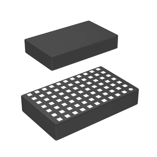
| 产品图片 |
|
| 产品型号 | LTM8042EV-1#PBF |
| PCN设计/规格 | |
| rohs | 无铅 / 符合限制有害物质指令(RoHS)规范要求 |
| 产品系列 | µModule® |
| 其它名称 | LTM8042EV1PBF |
| 功率(W) | 11W |
| 包装 | 托盘 |
| 参考设计库 | http://www.digikey.com/rdl/4294959899/4294959898/585http://www.digikey.com/rdl/4294959899/4294959898/586 |
| 大小/尺寸 | 0.59" 长 x 0.35" 宽 x 0.11" 高(15.0mm x 9.0mm x 2.8mm) |
| 安装类型 | 表面贴装 |
| 封装/外壳 | 77-BLGA |
| 工作温度 | -40°C ~ 125°C |
| 拓扑 | 升压,降压,降压-升压 |
| 效率 | - |
| 标准包装 | 170 |
| 特性 | 远程开/关,OTP,SCP |
| 特色产品 | http://www.digikey.com/product-highlights/cn/zh/linear-technology-umodule/1305http://www.digikey.cn/product-highlights/zh/ltm2884-usb-transceivers/52569 |
| 电压-输入(最大值) | 30V |
| 电压-输入(最小值) | 3V |
| 电压-输出 | 2 ~ 32 V |
| 电流-输出(最大值) | 350mA |
| 类型 | 恒定电流 |
| 认可 | - |
| 设计资源 | http://cds.linear.com/docs/38967http://www.linear.com/docs/30214 |
| 调光 | 模拟,PWM |
| 输出数 | 1 |
| 配用 | /product-detail/zh/DC1511A-B/DC1511A-B-ND/2428210/product-detail/zh/DC1511A-A/DC1511A-A-ND/2428209 |
| 重量 | 0.002 磅(0.91g) |


- 商务部:美国ITC正式对集成电路等产品启动337调查
- 曝三星4nm工艺存在良率问题 高通将骁龙8 Gen1或转产台积电
- 太阳诱电将投资9.5亿元在常州建新厂生产MLCC 预计2023年完工
- 英特尔发布欧洲新工厂建设计划 深化IDM 2.0 战略
- 台积电先进制程称霸业界 有大客户加持明年业绩稳了
- 达到5530亿美元!SIA预计今年全球半导体销售额将创下新高
- 英特尔拟将自动驾驶子公司Mobileye上市 估值或超500亿美元
- 三星加码芯片和SET,合并消费电子和移动部门,撤换高东真等 CEO
- 三星电子宣布重大人事变动 还合并消费电子和移动部门
- 海关总署:前11个月进口集成电路产品价值2.52万亿元 增长14.8%
PDF Datasheet 数据手册内容提取
LTM8042/LTM8042-1 µModule Boost LED Driver and Current Source FEATURES DESCRIPTION n True Color PWM™ with 3000:1 Dimming Ratio The LTM®8042 is a complete µModule® Boost LED Driver n Operates in Boost, Buck Mode or Buck-Boost Mode specifically designed to drive LEDs up to 1A, while the n Wide Input Voltage Range: LTM8042-1 drives up to 350mA. It combines a boost Operation from 3V to 30V power topology with a unique current loop to operate as Transient Protection to 40V a constant-current source. The PWM input provides as n Gate Driver for Optional PWM Dimming with much as 3000:1 LED dimming, while 10:1 analog dimming P-channel MOSFET can be accomplished by a single resistor or analog voltage n Adjustable Frequency: 250kHz to 2MHz applied to the CTL pin. As with any boost topology, the n Constant-Current and Constant-Voltage Regulation LTM8042/LTM8042-1 has an uninterrupted current path n Low Shutdown Current: <1μA between its input and output and is thus intolerant to a n RoHS Compliant Package with Gold Pad Finish short-circuit or overload from the output to ground. n Tiny, Low Profile (9mm × 15mm × 2.82mm) # WHITE LEDS LED CURRENT 12V 24V Surface Mount LGA Package IN IN 6 1A LTM8042 7 350mA LTM8042-1 APPLICATIONS 8 1A LTM8042 n Display Backlighting 9 350mA LTM8042-1 n Automotive and Avionic Lighting The LTM8042/LTM8042-1 is packaged in a thermally n Illumination enhanced, compact overmolded land grid array (LGA) n Scanners package. The LTM8042/LTM8042-1 is Pb-free and a L, LT, LTC, LTM, Linear Technology, the Linear logo and µModule are registered trademarks RoHS compliant. and True Color PWM is a trademark of Linear Technology Corporation. All other trademarks are the property of their respective owners. TYPICAL APPLICATION µModule Boost LED Driver, Driving 8 White LEDs at 1A Efficiency vs V IN UP TO 26.8V 97 16V TO 2V6IVN VCC LTM8042 9956 RUN LED+ 94 BSTIN/BKLED– TG %) PWM BSTOUT/BKIN CY ( 93 N 92 E SYNC 1A FICI 91 F TGEN E 90 SS 89 4.7µF RT GNDCTL 88 4.7µF 33.2k 87 fSW = 550kHz 16 17 18 19 20 21 22 23 24 25 26 VIN (V) 80421 TA01a 80421 TA01b 80421fb 1 For more information www.linear.com/LTM8042
LTM8042/LTM8042-1 ABSOLUTE MAXIMUM RATINGS PIN CONFIGURATION (Note 1) V , RUN, PWM, TGEN, BSTIN/BKLED– ...................40V BSTIN/BKLED– CC BSTOUT/BKIN, LED+ ................................................43V TG 7 CTL, SYNC ..................................................................6V VCC BANK 2 BANK 3 BANK 4 BANK 5 6 Internal Operating Temperature BSTOUT/BKIN LED+ 5 (Notes 3, 4) ...........................................–40°C to 125°C 4 Maximum Reflow Body Temperature ..................245°C BANK 1 Storage Temperature .............................–55°C to 125°C 3 TGEN GND 2 CTL 1 A B C D E F G H J K L RUN SYNC RT SS PWM LGA PACKAGE 77-LEAD (15mm × 9mm × 2.82mm) TJMAX = 125°C, θJA = 15.7°C/W, θJCtop = 13.6°C/W, θJCbottom = 4.5°C/W, θJB = 9.4°C/W θ VALUES DETERMINED PER JESD 51-12 WEIGHT = 1.1g ORDER INFORMATION PART MARKING* TEMPERATURE RANGE PART NUMBER PAD OR BALL FINISH DEVICE FINISH CODE PACKAGE TYPE MSL RATING (Note 4) LTM8042EV#PBF Au (RoHS) LTM8042V e4 LGA 3 –40°C to 125°C LTM8042IV#PBF Au (RoHS) LTM8042V e4 LGA 3 –40°C to 125°C LTM8042EV-1#PBF Au (RoHS) LTM8042V-1 e4 LGA 3 –40°C to 125°C LTM8042IV-1#PBF Au (RoHS) LTM8042V-1 e4 LGA 3 –40°C to 125°C Consult Marketing for parts specified with wider operating temperature • Recommended LGA and BGA PCB Assembly and Manufacturing ranges. *Device temperature grade is indicated by a label on the shipping Procedures: container. Pad or ball finish code is per IPC/JEDEC J-STD-609. www.linear.com/umodule/pcbassembly • Terminal Finish Part Marking: • LGA and BGA Package and Tray Drawings: www.linear.com/leadfree www.linear.com/packaging 80421fb 2 For more information www.linear.com/LTM8042
LTM8042/LTM8042-1 ELECTRICAL CHARACTERISTICS The l denotes the specifications which apply over the full internal operating temperature range, otherwise specifications are at T = 25°C. V = 5V, buck mode with 4Ω load. A CC SYMBOL PARAMETER CONDITIONS MIN TYP MAX UNITS V Minimum Input DC Voltage l 3 V CC(MIN) I LTM8042 LED Current CTL Open 0.9 1.05 A LED R = 6.81k 0.45 0.5 0.55 A CTL LTM8042-1 LED Current CTL Open 0.34 0.39 A R = 6.81k 0.17 0.20 A CTL V Open LED Clamp Voltage Boost Mode, LED+ Open 36 V CLAMP ∆I /I Output Current Line Regulation LTM8042, 6V < BSTOUT/BKIN < 30V 0.5 % OUT OUT LTM8042-1, 6V < BSTOUT/BKIN < 30V 0.5 % I V Supply Current PWM = 0V 4.2 mA QVCC CC RUN = 0V 0.1 1 µA f Switching Frequency RT = 90.9k 0.22 0.25 0.27 MHz SW RT = 22.1k 0.68 0.8 0.92 MHz RT = 6.04k 1.7 2 2.3 MHz I Soft-Start Pin Current SS = 0.5V, Out of Pin 6 9 12 µA SS f Synchronization Frequency Range 0.3 2.5 MHz SYNC I SYNC Pull-Down Current (Into the Pin) V = 2V 60 µA SYNC SYNC V SYNC Input Low 0.4 V SYNC(IL) V SYNC Input High 1.5 V SYNC(IH) I CTL Input Bias Current CTL = 0V, Flows Out of Pin 100 µA CTL V RUN Input Voltage High 1.5 V RUN(IH) V RUN Input Voltage Low 0.4 V RUN(IL) I RUN Pin Bias Current 60 100 µA RUN V PWM Input Voltage High 1.5 V PWM(IH) V PWM Input Voltage Low 0.4 V PWM(IL) I PWM Pin Bias Current 60 120 µA PWM V TG Output High Voltage Relative to LED+, 100k from LED+ to TG 0 V TG(OH) V TG Output Low Voltage Relative to LED+, 100k from LED+ to TG –7 V TG(OL) V TGEN Input Voltage High PWM = 0V 1.5 V TGEN(IH) V TGEN Input Voltage Low 0.4 V TGEN(IL) I TGEN Pin Bias Current 100 200 µA TGEN Note 1: Stresses beyond those listed under Absolute Maximum Ratings The LTM8042I/LTM8042I-1 are guaranteed to meet specifications over may cause permanent damage to the device. Exposure to any Absolute the full –40°C to 125°C internal operating temperature range. Note that Maximum Rating condition for extended periods may affect device the maximum internal temperature is determined by specific operating reliability and lifetime. conditions in conjunction with board layout, the rated package thermal Note 2: Absolute maximum voltage at V , RUN, PWM, TGEN, BSTIN/ resistance and other environmental factors. CC BKLED– pins is 40V for non-repetitive one second transients and 30V for Note 4: This device includes overtemperature protection that is intended continuous operation. to protect the device during momentary overload conditions. Junction Note 3: The LTM8042E/LTM8042E-1 are guaranteed to meet performance temperature will exceed the maximum internal operating temperature specifications from 0°C to 125°C ambient. Specifications over the full when overtemperature protection is active. Continuous operation above –40°C to 125°C internal operating temperature range are assured by the specified maximum operating junction temperature may impair device design, characterization and correlation with statistical process controls. reliability. 80421fb 3 For more information www.linear.com/LTM8042
LTM8042/LTM8042-1 TYPICAL PERFORMANCE CHARACTERISTICS T = 25°C, unless otherwise noted. A LTM8042 Efficiency vs V , Boost Operation, Efficiency vs V , Boost Operation, Efficiency vs V , Boost Operation, IN IN IN 6.8V at 1A LED String 10.1V at 1A LED String 13.4V at 1A LED String 90 95 94 89 94 88 92 93 87 90 92 %) %) %) CY ( 86 CY ( 88 CY ( 91 N 85 N N 90 EFFICIE 84 EFFICIE 86 EFFICIE 89 83 88 84 82 87 82 81 86 80 80 85 4 5 6 5 6 7 8 9 10 7 8 9 10 11 12 13 VIN (V) VIN (V) VIN (V) 80421 G01 80421 G02 80421 G03 Efficiency vs V , Boost Operation, Efficiency vs V , Boost Operation, Efficiency vs V , Boost Operation, IN IN IN 16.7V at 1A LED String 20.1V at 1A LED String 23.4V at 1A LED String 97 97 94 95 95 92 93 93 90 %) %) %) CY ( 88 CY ( 91 CY ( 91 N N N EFFICIE 86 EFFICIE 89 EFFICIE 89 84 87 87 82 85 85 80 83 83 8 9 10 11 12 13 14 15 16 11 12 13 14 15 16 17 18 19 12 13 14 15 16 17 18 19 20 21 22 VIN (V) VIN (V) VIN (V) 80421 G04 80421 G05 80421 G06 Efficiency vs VIN, Boost Operation, Efficiency vs VIN, Buck Mode, Efficiency vs VIN, Buck Mode, 26.8V at 1A LED String 3.5V at 1A LED String 6.8V at 1A LED String 97 89 94 96 95 87 92 94 85 90 %) %) %) CY ( 93 CY ( 83 CY ( 88 N 92 N N E E E FICI 91 FICI 81 FICI 86 F F F E E E 90 79 84 89 77 82 88 87 75 80 16 17 18 19 20 21 22 23 24 25 26 4 6 8 10121416182022242628303234 8 10 12 14 16 18 20 22 24 26 28 30 32 34 VIN (V) VIN (V) VIN (V) 80421 G07 80421 G08 80421 G09 80421fb 4 For more information www.linear.com/LTM8042
LTM8042/LTM8042-1 TYPICAL PERFORMANCE CHARACTERISTICS T = 25°C, unless otherwise noted. A LTM8042 Efficiency vs V , Buck Mode, Efficiency vs V , Buck Mode, Efficiency vs V , Buck Mode, IN IN IN 10.1V at 1A LED String 13.4V at 1A LED String 16.7V at 1A LED String 95 97 97 94 96 96 93 95 95 92 94 94 %) %) %) Y ( 91 Y ( 93 Y ( 93 NC 90 NC 92 NC 92 EFFICIE 89 EFFICIE 91 EFFICIE 91 88 90 90 87 89 89 86 88 88 85 87 87 12 14 16 18 20 22 24 26 28 30 32 34 15 17 19 21 23 25 27 29 31 33 19 21 23 25 27 29 31 33 VIN (V) VIN (V) VIN (V) 80421 G10 80421 G11 80421 G12 Efficiency vs V , Buck-Boost Efficiency vs V , Buck-Boost Efficiency vs V , Buck-Boost IN IN IN Mode, 3.6V at 1A LED String Mode, 6.8V at 1A LED String Mode, 10.1V at 1A LED String 85 90 87 86 80 85 85 %) 75 %) %) Y ( Y ( Y ( 84 C C C N 70 N 80 N E E E CI CI CI 83 EFFI 65 EFFI EFFI 82 75 60 81 55 70 80 4 6 8 10 12 14 16 18 20 22 24 26 28 30 8 10 12 14 16 18 20 22 24 26 12 13 14 15 16 17 18 19 20 21 22 23 24 VIN (V) VIN (V) VIN (V) 80421 G13 80421 G14 80421 G15 Efficiency vs V , Buck-Boost Maximum LED Current IN Mode, 13.4V at 1A LED String vs Input Voltage, Boost Operation 90 1200 89 88 A)1000 m 87 T ( %) EN 800 ENCY ( 8856 D CURR 600 EFFICI 84 UM LE 400 71.04.V9V A AT T1 A1A 83 M 14.5V AT 1A 82 AXI 18.1V AT 1A M 200 21.4V AT 1A 81 24.8V AT 1A 28.2V AT 1A 80 0 15 16 17 18 19 20 0 5 10 15 20 25 30 VIN (V) INPUT VOLTAGE (V) 80421 G16 80421 G17 80421fb 5 For more information www.linear.com/LTM8042
LTM8042/LTM8042-1 TYPICAL PERFORMANCE CHARACTERISTICS T = 25°C, unless otherwise noted. A LTM8042 Maximum LED Current Maximum LED Current vs Input vs V , Buck Mode Voltage, Buck-Boost Mode IN 1000 1200 900 800 A)1000 m mA)700 ENT ( 800 T (600 RR N U LED CURRE435000000 371..084.VV9V AA ATT T11 AA1A XIMUM LED C 460000 711.044..V95VV A AAT TT1 A11AA 200 14.5V AT 1A A 18.1V AT 1A 18.1V AT 1A M 200 21.4V AT 1A 100 21.4V AT 1A 24.8V AT 1A 0 24.8V AT 1A 0 28.2V AT 1A 0 5 10 15 20 25 30 0 10 20 30 40 VIN (N) INPUT VOLTAGE (V) 80421 G18 80421 G19 Junction Temperature Rise Quiescent Current vs Load, Boost Operation, LED Current vs CTL Voltage vs Input Voltage, Open LED 8.3V at 1A LED String 40 25 100 35 SCALING (%) 8600 RRENT (mA) 3205 URE (°C) 2105 5VIN LED CURRENT 2400 QUIESCENT CU 121005 TEMPERAT 150 5 0 0 0 0 200 400 600 800 1000 1200 0 5 10 15 20 25 30 0 200 400 600 800 1000 ADJUST VOLTAGE (mV) INPUT VOLTAGE (V) LED CURRENT (mA) 80421 G20 80421 G21 80421 G22 Junction Temperature Rise Junction Temperature Rise Junction Temperature Rise vs Load, Boost Operation, vs Load, Boost Operation, vs Load, Boost Operation, 10.9V at 1A LED String 13.6V at 1A LED String 18.1V at 1A LED String 20 25 35 18 30 16 20 RE (°C) 1142 7VIN RE (°C) 15 8VIN RE (°C) 2205 9VIN U U U AT 10 AT AT PER 8 PER 10 PER 15 M M M TE 6 TE TE 10 4 5 5 2 0 0 0 0 200 400 600 800 1000 0 200 400 600 800 1000 0 200 400 600 800 1000 LED CURRENT (mA) LED CURRENT (mA) LED CURRENT (mA) 80421 G23 80421 G24 80421 G25 80421fb 6 For more information www.linear.com/LTM8042
LTM8042/LTM8042-1 TYPICAL PERFORMANCE CHARACTERISTICS T = 25°C, unless otherwise noted. A LTM8042 Junction Temperature Rise vs Load, Junction Temperature Rise vs Load, Junction Temperature Rise vs Load, Buck Mode, 2.9V at 1A LED String Buck Mode, 3.8V at 1A LED String Buck Mode, 8.3V at 1A LED String 18 18 25 16 16 14 14 20 URE (°C) 1102 24VIN URE (°C) 1102 24VIN URE (°C) 15 24VIN AT AT AT R 8 R 8 R TEMPE 6 12VIN TEMPE 6 12VIN TEMPE 10 12VIN 4 4 5 2 2 0 0 0 0 200 400 600 800 1000 0 200 400 600 800 1000 0 200 400 600 800 1000 LED CURRENT (mA) LED CURRENT (mA) LED CURRENT (mA) 80421 G26 80421 G27 80421 G28 Junction Temperature Rise vs Load, Junction Temperature Rise vs Load, Junction Temperature Rise vs Load, Buck Mode, 10.9V at 1A LED String Buck Mode, 13.6V at 1A LED String Buck Mode, 18.1V at 1A LED String 25 30 25 25 20 20 RE (°C) 15 24VIN RE (°C) 20 24VIN RE (°C) 15 24VIN U U U T T 15 T A A A R R R PE 10 PE PE 10 EM EM 10 EM T T T 5 5 5 0 0 0 0 200 400 600 800 1000 0 200 400 600 800 1000 0 200 400 600 800 1000 LED CURRENT (mA) LED CURRENT (mA) LED CURRENT (mA) 80421 G29 80421 G30 80421 G31 Junction Temperature Rise Junction Temperature Rise Junction Temperature Rise vs Load, Buck-Boost Mode, vs Load, Buck-Boost Mode, vs Load, Buck-Boost Mode, 2.9V at 1A LED String 3.8V at 1A LED String 8.3V at 1A LED String 25 30 40 35 25 20 5VIN 30 URE (°C) 15 24VIN URE (°C) 20 24VIN URE (°C) 25 12VIN AT AT 15 AT 20 TEMPER 10 5VIN TEMPER 10 12VIN TEMPER 15 10 5 5 12VIN 5 0 0 0 0 200 400 600 800 1000 0 200 400 600 800 1000 0 200 400 600 800 1000 LED CURRENT (mA) LED CURRENT (mA) LED CURRENT (mA) 80421 G32 80421 G33 80421 G34 80421fb 7 For more information www.linear.com/LTM8042
LTM8042/LTM8042-1 TYPICAL PERFORMANCE CHARACTERISTICS T = 25°C, unless otherwise noted. A LTM8042 Junction Temperature Rise Junction Temperature Rise Junction Temperature Rise vs Load, Buck-Boost Mode, vs Load, Buck-Boost Mode, vs Load, Buck-Boost Mode, 10.9V at 1A LED String 13.6V at 1A LED String 15.5V at 350mA LED String 50 60 25 45 50 40 20 URE (°C) 3350 12VIN URE (°C) 40 12VIN 16VIN URE (°C) 15 12VIN AT 25 AT 30 AT R R R PE 20 PE PE 10 TEM 15 TEM 20 TEM 10 5 10 5 0 0 0 0 200 400 600 800 1000 0 200 400 600 800 1000 0 50 100 150 200 250 300 350 LED CURRENT (mA) LED CURRENT (mA) LED CURRENT (mA) 80421 G35 80421 G36 80421 G37 LTM8042/LTM8042-1 RUN Pin Current vs Voltage 160 140 120 A) T (µ100 N E R 80 R U C N 60 U R 40 20 0 0 10 20 30 40 RUN VOLTAGE (V) LTM8042-1 80421 G38 Efficiency vs V , Boost Operation, Efficiency vs V , Boost Operation, Efficiency vs V , Boost Operation, IN IN IN 6.7V at 350mA LED String 9.7V at 350mA LED String 12.6V at 350mA LED String 95 95 95 90 90 90 %) 85 %) 85 %) 85 Y ( Y ( Y ( C C C N 80 N 80 N 80 E E E CI CI CI EFFI 75 EFFI 75 EFFI 75 70 70 70 65 65 65 2 3 4 5 6 2.5 4.5 6.5 8.5 3 5 7 9 11 VIN (V) VIN (V) VIN (V) 80421 G39 80421 G40 80421 G41 80421fb 8 For more information www.linear.com/LTM8042
LTM8042/LTM8042-1 TYPICAL PERFORMANCE CHARACTERISTICS T = 25°C, unless otherwise noted. A LTM8042-1 Efficiency vs V , Boost Operation, Efficiency vs V , Boost Operation, Efficiency vs V , Boost Operation, IN IN IN 15.6V at 350mA LED String 18.6V at 350mA LED String 21.6V at 350mA LED String 95 95 95 90 90 90 %) 85 %) 85 %) 85 Y ( Y ( Y ( NC 80 NC 80 NC 80 CIE CIE CIE EFFI 75 EFFI 75 EFFI 75 70 70 70 65 65 65 4 5 6 7 8 9 10 11 12 13 14 15 4 5 6 7 8 9 101112131415161718 5 6 7 8 9 10 11 12 13 14 15 16 17 18 VIN (V) VIN (V) VIN (V) 80421 G42 80421 G43 80421 G44 Efficiency vs V , Boost Operation, Efficiency vs V , Buck Mode, Efficiency vs V , Buck Mode, IN IN IN 24.8V at 350mA LED String 3.7V at 350mA LED String 6.7V at 350mA LED String 93 93 96 91 91 94 89 89 92 %) 87 %) 87 %) 90 NCY ( 85 NCY ( 85 NCY ( 88 EFFICIE 8813 EFFICIE 8813 EFFICIE 86 84 79 79 77 77 82 75 75 80 6 8 10 12 14 16 18 20 22 24 4 6 8 101214161820222426283032 8 10 12 14 16 18 20 22 24 26 28 30 32 34 VIN (V) VIN (V) VIN (V) 80421 G45 80421 G46 80421 G47 Efficiency vs V , Buck Mode, Efficiency vs V , Buck Mode, Efficiency vs V , Buck Mode, IN IN IN 9.7V at 350mA LED String 12.6V at 350mA LED String 15.6V at 350mA LED String 98 97 97 96 95 95 94 %) 92 %) 93 %) 93 Y ( 90 Y ( Y ( NC NC 91 NC 91 CIE 88 CIE CIE EFFI 86 EFFI 89 EFFI 89 84 87 87 82 80 85 85 11 13 15 17 19 21 23 25 27 29 31 33 14 16 18 20 22 24 26 28 30 32 17 19 21 23 25 27 29 31 33 VIN (V) VIN (V) VIN (V) 80421 G48 80421 G49 80421 G50 80421fb 9 For more information www.linear.com/LTM8042
LTM8042/LTM8042-1 TYPICAL PERFORMANCE CHARACTERISTICS T = 25°C, unless otherwise noted. A LTM8042-1 Efficiency vs V , Buck Mode, Efficiency vs V , Buck-Boost Efficiency vs V , Buck-Boost IN IN IN 18.6V at 350mA LED String Mode, 3.7V at 350mA LED String Mode, 6.7V at 350mA LED String 97 90 90 80 85 95 80 70 75 %) 93 %) 60 %) Y ( Y ( 50 Y ( 70 NC 91 NC NC 65 EFFICIE 89 EFFICIE 4300 EFFICIE 60 55 20 50 87 10 45 85 0 40 21 23 25 27 29 31 33 0 10 20 30 40 0 5 10 15 20 25 30 VIN (V) VIN (V) VIN (V) 80421 G51 80421 G52 80421 G53 Efficiency vs V , Buck-Boost Efficiency vs V , Buck-Boost Efficiency vs V , Buck-Boost IN IN IN Mode, 9.7V at 350mA LED String Mode, 12.6V at 350mA LED String Mode, 15.6V at 350mA LED String 90 90 88 85 86 85 84 80 %) 75 %) 80 %) 82 Y ( Y ( Y ( 80 C C C N 70 N 75 N CIE CIE CIE 78 EFFI 65 EFFI 70 EFFI 76 60 74 65 55 72 50 60 70 0 5 10 15 20 25 30 0 5 10 15 20 25 0 10 15 20 VIN (V) VIN (V) VIN (V) 80421 G54 80421 G55 80421 G56 Efficiency vs V , Buck-Boost Maximum LED Current vs Input Maximum LED Current vs Input IN Mode, 18.6V at 350mA LED String Voltage, Boost Operation Voltage, Buck Mode 87 400 400 350 350 85 A) A) m 300 m300 T ( T ( ENCY (%) 8813 D CURREN 220500 D CURREN220500 EFFICI 79 UM LE 150 UM LE150 3.2V AT 350mA M 6.3V AT 350mA M 6.3V AT 350mA AXI 100 15.5V AT 350mA AXI100 9.4V AT 350mA 77 M 18.6V AT 350mA M 12.4V AT 350mA 50 21.7V AT 350mA 50 15.5V AT 350mA 24.8V AT 350mA 18.6V AT 350mA 75 0 0 5 7 9 11 13 15 0 5 10 15 20 25 0 10 20 30 40 VIN (V) INPUT VOLTAGE (V) INPUT VOLTAGE (V) 80421 G57 80421 G58 80421 G59 80421fb 10 For more information www.linear.com/LTM8042
LTM8042/LTM8042-1 TYPICAL PERFORMANCE CHARACTERISTICS T = 25°C, unless otherwise noted. A LTM8042-1 Maximum LED Current vs Input Quiescent Current vs Input Voltage, Buck-Boost Mode LED Current vs CTL Voltage Voltage, Open LED 400 120 80 350 70 mA)300 %)100 A) 60 MAXIMUM LED CURRENT (121200550000 3691...2234.VVV4V AAA ATTT T333 55530005mmm0mAAAA LED CURRENT SCALING ( 42680000 QUIESCENT CURRENT (m 45230000 50 10 15.5V AT 350mA 18.6V AT 350mA 0 0 0 0 10 20 30 40 0 200 400 600 800 1000 1200 0 5 10 15 20 25 30 35 INPUT VOLTAGE (V) CTL VOLTAGE (mV) INPUT VOLTAGE (V) 80421 G60 80421 G61 80421 G62 Junction Temperature Rise Junction Temperature Rise Junction Temperature Rise vs Load, Boost Operation, vs Load, Boost Operation, vs Load, Boost Operation, 6.8V at 350mA LED String 9.4V at 350mA LED String 11.2V at 350mA LED String 5 7 8 6 7 4 6 URE (°C) 3 5VIN URE (°C) 54 5VIN URE (°C) 5 5VIN AT AT AT 4 MPER 2 MPER 3 MPER 3 TE TE 2 TE 2 1 1 1 0 0 0 0 50 100 150 200 250 300 350 0 50 100 150 200 250 300 350 0 50 100 150 200 250 300 350 LED CURRENT (mA) LED CURRENT (mA) LED CURRENT (mA) 80421 G63 80421 G64 80421 G65 Junction Temperature Rise Junction Temperature Rise Junction Temperature Rise vs Load, Boost Operation, vs Load, Buck Mode, vs Load, Buck Mode, 15.5V at 350mA LED String 2.3V at 350mA LED String 3.2V at 350mA LED String 14 10 6 9 12 5 8 24VIN RE (°C) 108 5VIN RE (°C) 67 RE (°C) 4 12VIN U U U AT AT 5 AT 3 PER 6 PER 4 12VIN PER TEM 4 TEM 3 TEM 2 5VIN 2 1 2 1 0 0 0 0 50 100 150 200 250 300 350 0 50 100 150 200 250 300 350 0 50 100 150 200 250 300 350 LED CURRENT (mA) LED CURRENT (mA) LED CURRENT (mA) 80421 G66 80421 G67 80421 G68 80421fb 11 For more information www.linear.com/LTM8042
LTM8042/LTM8042-1 TYPICAL PERFORMANCE CHARACTERISTICS T = 25°C, unless otherwise noted. A LTM8042-1 Junction Temperature Rise Junction Temperature Rise Junction Temperature Rise vs Load, Buck Mode, vs Load, Buck Mode, vs Load, Buck Mode, 6.8V at 350mA LED String 9.4V at 350mA LED String 11.2V at 350mA LED String 12 14 14 12 12 10 TEMPERATURE (°C) 846 24VIN 12VIN TEMPERATURE (°C) 10846 24VIN TEMPERATURE (°C) 10846 24VIN 2 2 2 0 0 0 0 50 100 150 200 250 300 350 0 50 100 150 200 250 300 350 0 50 100 150 200 250 300 350 LED CURRENT (mA) LED CURRENT (mA) LED CURRENT (mA) 80421 G69 80421 G70 80421 G71 Junction Temperature Rise Junction Temperature Rise Junction Temperature Rise vs Load, Buck Mode, vs Load, Buck-Boost Mode, vs Load, Buck-Boost Mode, 15.5V at 350mA LED String 2.3V at 350mA LED String 3.2V at 350mA LED String 14 10 12 12 24VIN 10 8 24VIN RE (°C) 108 24VIN RE (°C) 6 12VIN RE (°C) 8 12VIN U U U T T T 6 A A A PER 6 PER 4 PER EM EM EM 4 T 4 T T 2 5VIN 2 5VIN 2 3.3VIN 3.3VIN 0 0 0 0 50 100 150 200 250 300 350 0 50 100 150 200 250 300 350 0 50 100 150 200 250 300 350 LED CURRENT (mA) LED CURRENT (mA) LED CURRENT (mA) 80421 G72 80421 G73 80421 G74 Junction Temperature Rise Junction Temperature Rise vs Load, Buck-Boost Mode, vs Load, Buck-Boost Mode, 6.8V at 350mA LED String 9.4V at 350mA LED String 12 16 14 10 12VIN 12 URE (°C) 8 URE (°C) 10 12VIN T 6 T 8 A A ER 5VIN ER 5VIN EMP 4 EMP 6 T T 4 2 2 0 0 0 50 100 150 200 250 300 350 0 50 100 150 200 250 300 350 LED CURRENT (mA) LED CURRENT (mA) 80421 G75 80421 G76 80421fb 12 For more information www.linear.com/LTM8042
LTM8042/LTM8042-1 TYPICAL PERFORMANCE CHARACTERISTICS T = 25°C, unless otherwise noted. A LTM8042-1 Junction Temperature Rise Junction Temperature Rise vs Load, Buck-Boost Mode, vs Load, Buck-Boost Mode, 11.2V at 350mA LED String 15.5V at 350mA LED String 18 30 16 25 14 E (°C) 12 12VIN E (°C) 20 UR 10 UR T T 15 ERA 8 ERA 12VIN EMP 6 5VIN EMP 10 T T 5VIN 4 5 2 0 0 0 50 100 150 200 250 300 350 0 50 100 150 200 250 300 350 LED CURRENT (mA) LED CURRENT (mA) 80421 G77 80421 G78 PIN FUNCTIONS GND (Bank 1): Signal and Power Return. Tie these pads LED+ (Bank 5): Connect this to the anode of the LED to a local ground plane below the LTM8042/LTM8042-1 string. This can also be connected to the PWM dimming and the circuit components. In most applications, the MOSFET if used. bulk of the heat flow out of the LTM8042/LTM8042-1 is RUN (Pin F1): Module Enable. Tie to 1.5V or higher to through these pads, so the printed circuit design has a enable the LTM8042/LTM8042-1 or 0.4V or less to dis- large impact on the thermal performance of the part. See able device. the PCB Layout and Thermal Considerations sections for more details. SYNC (Pin G1): Frequency Synchronization Pin. Tie an external clock signal here. The RT resistor should be V (Bank 2): Internal Housekeeping Power for the CC chosen to program a switching frequency that is 20% LTM8042/LTM8042-1. Connect to an external power slower than SYNC pulse frequency. Tie the SYNC pin to source between 3V and 30V. The LTM8042/LTM8042-1 GND if this feature is not used. can withstand transients of 40V. RT (Pin H1): Timing Resistor Pin. Used to program the BSTIN/BKLED– (Bank 3): Power Input for Boost Operation, switching frequency of the LTM8042/LTM8042-1 by con- as Well as the Cathode Connection for the LED String in necting a resistor from this pin to GND. The Applications Buck Mode. If the LTM8042/LTM8042-1 is used in boost Information section of the data sheet includes a table mode, these pins must be locally decoupled. to determine the resistance value based on the desired BSTOUT/BKIN (Bank 4): Output of the Boost Converter, switching frequency. Minimize capacitance at this pin. as Well as the Input for Buck Mode. If the LTM8042/ SS (Pin J1): Soft-Start Pin. Place a soft-start capacitor LTM8042-1 is used in buck mode, these pins must be here. Leave the pin open if not used. locally decoupled. 80421fb 13 For more information www.linear.com/LTM8042
LTM8042/LTM8042-1 PIN FUNCTIONS TG (Pin J7): Top Gate Driver Output. In response to an CTL (Pin L2): LED Current Adjustment Pin. Apply a volt- active high PWM signal, this pin will drive the gate of an age between approximately 1V and 0V to modulate the external series P-channel MOSFET device low. An inter- LED+ output current, or tie a resistor to GND to modulate nal 7V clamp protects the PFET gate. This pin can also the LED+ current. CTL is internally tied to a 2V precision be used to disconnect the load when RUN is pulled low. reference via a 20k 1% resistor. Leave floating if unused. Leave TG unconnected if not used. Do not drive this pin TGEN (Pin L3): Top Gate (TG) Enable Input Pin. Tie to 1.5V with an external source. or higher to enable the P-channel MOSFET driver function. PWM (Pin K1): Pulse Width Modulation Input Pin. A low Tie the TGEN pin to ground if the TG function is not used. signal turns off the LED string, disables the main switch There is an internal 40k resistor from TGEN to GND. and pulls the TG pin high. Drive above 1.55V to deliver current to the output. Tie the PWM pin to the RUN pin if not used. There is an equivalent 50k resistor from PWM pin to ground internally. BLOCK DIAGRAM BSTIN/BKLED– 4.7µH BSTOUT/BKIN 0.1µF 1M 0.1µF RSNS 0.10Ω (LTM8042) VCC 0.27Ω (LTM8042-1) LED+ OPEN LED 0.1µF PROTECTION (1V THRESHOLD) 28.0k CURRENT RUN MODE LED CURRENT SENSE+ CONTROLLER SS CURRENT SENSE– TG PWM 2V 20.0k 50k 1% SYNC GND RT TGEN CTL 80421 BD 80421fb 14 For more information www.linear.com/LTM8042
LTM8042/LTM8042-1 OPERATION The LTM8042/LTM8042-1 is a complete, full featured, The other way the LTM8042/LTM8042-1 can dim a LED current mode regulator specifically designed to drive light array is by pulse width modulation using the PWM pin emitting diodes (LEDs) or other loads where a constant and an optional external P-channel MOSFET. The external current up to 1A (350mA for the LTM8042-1) is required. P-channel MOSFET can be conveniently operated by the integrated gate driver at pin TG. The gate drive function The LTM8042/LTM8042-1 can operate in any of three LED can be enabled or disabled by the TGEN pin. drive topologies: boost, buck mode and buck-boost mode. The device features both analog and PWM dimming, a PWM If the PWM pin is pulled high, the part operates normally. If P-channel MOSFET driver, and a suite of control functions: the PWM pin is unconnected or pulled low, the LTM8042/ RUN control, soft-start, user programmable switching LTM8042-1 stops switching and the internal control cir- frequency, and external frequency synchronization. cuitry is held in its present state. This way, the LTM8042/ LTM8042-1 “remembers” the current sourced from the Operation can be best understood by referring to the LED+ output until PWM is pulled high again. This leads to Block Diagram. The power stage is a boost converter that a highly linear relationship between pulse width and output regulates the output current by reading the voltage across light, allowing for a large and accurate dimming range. a power sense resistor that is in series with the output. The RUN pin is used to deactivate the LTM8042/LTM8042-1. As with any boost topology, there is an uninterrupted cur- When the RUN pin is pulled to a logic low state, the device rent path between the input and output terminals. Current is shut down and draws typically less than 1µA of current. between these two terminals is not limited, so the device is intolerant to a short-circuit or overload from any of the The SS pin is used to limit inrush current during start-up. output terminals (LED+, BSTOUT/BKIN) to GND. The LTM8042/LTM8042-1 integrates a current source with this function, so only a capacitor is necessary to establish There are two ways to dim a LED with the LTM8042/ the soft-start characteristics of the output current. LTM8042-1. One way is to adjust the current on the LED array by setting the analog voltage on the CTL pin. The The switching frequency is set by applying a single resistor CTL pin is internally pulled up to a precision 2V reference from the RT pin to GND, allowing operation anywhere from through a 1% 20k resistor. Leaving the CTL pin floating 250kHz to 2MHz, and the SYNC pin allows synchroniza- sets the LED pin current to 1A. Reducing the voltage below tion to an external source between 300kHz and 2.5MHz. 1.1V on the CTL pin proportionally reduces the current flowing out of LED+. This can be accomplished by con- necting a resistor from the CTL pin to GND, forming a divider network with the internal 20k resistor, or by driving the CTL pin directly to a voltage source, such as a DAC. 80421fb 15 For more information www.linear.com/LTM8042
LTM8042/LTM8042-1 APPLICATIONS INFORMATION For most applications, the design process is straight Setting the Switching Frequency forward, summarized as follows: The LTM8042/LTM8042-1 uses a constant frequency 1. Decide whether the LTM8042/LTM8042-1 should oper- architecture that can be programmed over a 250kHz to ate in boost, buck, or buck-boost mode. 2MHz range with a single external timing resistor from the RT pin to ground. Table 7 shows suggested R selections 2. Look at Tables 1 through 6 and find the line that best T for a variety of switching frequencies. matches the input and output conditions of the system under consideration. Table 7. Switching Frequency vs R T 3. Connect C , C , C and R as indicated in the SWITCHING FREQUENCY (kHz) RT (kΩ) IN OUT VCC T appropriate table. 250 86.6 500 37.4 4. Connect the remaining pins as needed by the system 800 21.0 requirements. 1000 15.8 While these component combinations have been tested 1500 9.09 for proper operation, it is incumbent upon the user to 2000 6.04 verify proper operation over the intended system’s line, The other way to set the operating frequency of the load and environmental conditions. LTM8042/LTM8042-1 is to drive the SYNC pin with an If the desired LED current is not listed in Tables 1 through 6, external signal. For proper operation, a resistor should be set it by applying the proper voltage the CTL pin. Graphs connected at the RT pin and be able to generate a switch- of the LTM8042/LTM8042-1 LED current scaling vs CTL ing frequency 20% lower than the external clock when the voltage are given in the Typical Performance Character- external clock is absent. istics section. If a voltage source is not available to drive In general, a lower switching frequency should be used the CTL pin, a resistor may be applied from the CTL pin where either very high or very low switching duty cycle to GND. The CTL pin is internally pulled up to a 2V refer- operation is required, or high efficiency is desired. Selection ence voltage through a 20k resistor (please see the Block of a higher switching frequency will allow use of smaller Diagram for details). value external components and yield a smaller solution size and profile. Open LED Protection The LTM8042/LTM8042-1 has internal open LED circuit Operating Modes protection. If the LED is absent or fails open, the LTM8042/ The LTM8042/LTM8042-1 employs a ground referred LTM8042-1 clamps the voltage on the LED+ and BSTOUT/ power switch to implement a boost power switching BKIN pin to protect the output against overvoltage. The circuit. As such, it can be used to implement the three internal boost switching converter then regulates its most popular LED driving topologies: boost, buck mode, output to 36V. In buck mode, the full open LED voltage and buck-boost mode. Example layouts of each operating is stood off by the internal power Schottky diode. At high mode are given in Figures 2 through 4 and schematics are operating temperatures, the power Schottky reverse leak- shown in the Typical Applications section. age current will rise. This increases the power dissipation within the diode, which raises the junction temperature. This temperature rise can be large, so care needs to be taken at high operating temperatures. 80421fb 16 For more information www.linear.com/LTM8042
LTM8042/LTM8042-1 APPLICATIONS INFORMATION Which mode to use depends upon the operating condi- The minimum PWM on or off-time will depend on the tions. Boost is generally selected when the voltage across choice of operating frequency through the RT input pin or the LED string is always higher than the input voltage. Buck the SYNC pin. When using the SYNC function, the SYNC mode is the dual of boost, used when the voltage across and PWM signals must have the rising edges aligned to the LED string is always lower than V . Finally, buck-boost achieve the optimized high PWM dimming ratio. For best IN mode is used when the V can vary both above and below current accuracy, the minimum PWM low or high time IN the voltage across the LED string. should be at least six switching cycles (3μs for ƒ = SW 2MHz). The maximum PWM period is determined by the The land grid array of the LTM8042/LTM8042-1 is designed system. The maximum PWM dimming ratio (PWM ) to conveniently accommodate all three operating modes. RATIO can be calculated from the maximum PWM period (T ) Please refer to the PCB Layout section for suggested MAX and the minimum PWM pulse width (T ) as follows: examples of how to lay out each operating mode. MIN T Dimming Control PWMRATIO = MAX (1) T MIN There are two methods to control the current source for A set of values that give a 3000:1 dimming ratio, for ex- dimming using the LTM8042/LTM8042-1. One method ample, would be a switching frequency of ƒ = 2MHz, uses the PWM pin to modulate the current source between SW T = 9ms and T = 3μs. Equation (1) becomes: zero and full current to achieve a precisely programmed MAX MIN average current. To make this method of current control PWM = 9ms/3μs = 3000:1 RATIO more accurate, the switch demand current is internally The second method of dimming control uses the CTL pin stored during the quiescent phase (PWM low). This feature to linearly adjust the current sense threshold during the minimizes recovery time when the PWM signal returns PWM high state. When the CTL pin voltage is less than high. When using PWM dimming, use a P-channel MOSFET 1V, the LED current is: disconnect switch in the LED current path (see Figure 1) to prevent the output capacitor from discharging during ILED =VCTL the PWM off-time. Enable this function by pulling TGEN When V is higher than 1.1V, the LED current is clamped CTL above 1.5V. to 1A. The LED current programming feature can be used in LTM8042 VIN VCC LED+ conjunction with the PWM to possibly increase the total BSTIN/BKLED– dimming range by an additional factor of ten. RUN TG TGEN BSTOUT/BKIN PWM SYNC SS RT GND CTL 80421 TA01a Figure 1. The LTM8042/LTM8042-1 Can Control a P-Channel PWM Switch 80421fb 17 For more information www.linear.com/LTM8042
LTM8042/LTM8042-1 APPLICATIONS INFORMATION PCB Layout Most of the headaches associated with PCB layout have 4. Place the C , C and C capacitors such that their IN VCC OUT been alleviated or even eliminated by the high level of ground current flows directly adjacent to or underneath integration of the LTM8042/LTM8042-1. The device is the LTM8042/LTM8042-1. nevertheless a switching power supply, and care must be 5. Connect all of the GND connections to as large a copper taken to minimize EMI and ensure proper operation. Even pour or plane area as possible on the top layer. Avoid with the high level of integration, you may fail to achieve breaking the ground connection between the external specified operation with a haphazard or poor layout. See components and the LTM8042/LTM8042-1. Figures 2, 3 and 4 for suggested layouts of boost, buck and buck-boost operating modes. Use vias to connect the GND copper area to the board’s internal ground planes. Liberally distribute these GND vias Ensure that the grounding and heat sinking are acceptable. to provide both a good ground connection and thermal A few rules to keep in mind are: path to the internal planes of the printed circuit board. 1. Place the R resistor as close as possible to its re- Pay attention to the location and density of the thermal T spective pins. vias in Figures 2 through 4. The LTM8042/LTM8042-1 can benefit from the heat sinking afforded by vias that 2. Place the C and C capacitor as close as possible IN VCC connect to internal GND planes at these locations, due to to the V and GND connections of the LTM8042/ IN their proximity to internal power handling components. LTM8042-1. The optimum number of thermal vias depends upon the 3. Place the COUT capacitor as close as possible to the printed circuit board design. For example, a board might BSTOUT/BKIN or BSTIN/BKLED– and GND connection use very small via holes. It should employ more thermal of the LTM8042/LTM8042-1. vias than a board that uses larger holes. TO LED STRING GND CIN COUT LED+ VIN BSTIN/BKLED– TG VCC LED+ CVCC BSTOUT/BKIN GND TGEN CTL 80421 F02 R S S P GND UN YN S WM C RT THERMAL VIAS TO GROUND PLANE Figure 2. Suggested Layout for Boost Operation 80421fb 18 For more information www.linear.com/LTM8042
LTM8042/LTM8042-1 APPLICATIONS INFORMATION TO LED STRING VIN COUT VIN LED+ CVCC CIN BSTIN/BKLED– TG VCC LED+ BSTOUT/BKIN GND TGEN CTL 80421 F03 R S S P GND UN YN S WM C RT THERMAL VIAS TO GROUND PLANE Figure 3. Suggested Layout for Buck Mode TO LED STRING TO LED STRING COUT1 COUT2 LED+ CIN VIN BSTIN/BKLED– TG VCC LED+ CVCC BSTOUT/BKIN TGEN CTL 80421 F04 R S S P GND UN YN S WM C RT THERMAL VIAS TO GROUND PLANE Figure 4. Suggested Layout for Buck-Boost Mode 80421fb 19 For more information www.linear.com/LTM8042
LTM8042/LTM8042-1 APPLICATIONS INFORMATION Table 1. LTM8042 Recommended Values and Configuration for Boost (T = 25°C) A LED V STRING IN RANGE C C VOLTAGE LED RT f IN OUT (BSTIN/ (BSTIN/BKLED– (BSTOUT/BKIN (LED+ TO STRING (OPTI- (OPTI- RT f BKLED–) V TO GND) TO GND) GND) CURRENT R MAL) MAL) (MIN) (MAX) CC CTL 3V to 3.6V Connect to BSTIN/BKLED– 1µF 0805 X7R 10V 1µF 0805 X7R 10V 4V to 6V 35mA 523 86.6k 250k 37.4k 500k 3V to 5.1V Connect to BSTIN/BKLED– 1µF 0805 X7R 10V 1µF 0805 X7R 10V 6V to 9V 35mA 523 76.8k 275k 37.4k 500k 3V to 6.3V Connect to BSTIN/BKLED– 1µF 0805 X7R 10V 1µF 0805 X7R 16V 8V to 12V 35mA 523 69.8k 300k 37.4k 500k 3V to 9.3V Connect to BSTIN/BKLED– 1µF 0805 X7R 10V 1µF 0805 X7R 16V 12V to 16V 35mA 523 48.7k 400k 30.1k 600k 3V to 10V Connect to BSTIN/BKLED– 1µF 0805 X7R 10V 1µF 0805 X7R 25V 15V to 21V 35mA 523 37.4k 500k 27.4k 650k 3V to 12.6V Connect to BSTIN/BKLED– 1µF 0805 X7R 16V 1µF 0805 X7R 25V 18V to 24V 35mA 523 33.2k 550k 24.9k 700k 3.7V to 15V Connect to BSTIN/BKLED– 1µF 0805 X7R 16V 1µF 0805 X7R 50V 24V to 32V 35mA 523 30.1k 600k 24.9k 700k 3V to 3.85V Connect to BSTIN/BKLED– 4.7µF 1206 X7R 10V 2.2µF 1206 X7R 10V 4V to 6V 100mA 1.30k 86.6k 250k 37.4k 500k 3V to 5.6V Connect to BSTIN/BKLED– 4.7µF 1206 X7R 10V 2.2µF 1206 X7R 10V 6V to 9V 100mA 1.30k 76.8k 275k 37.4k 500k 3V to 7V Connect to BSTIN/BKLED– 4.7µF 1206 X7R 10V 2.2µF 1206 X7R 16V 8V to 12V 100mA 1.30k 69.8k 300k 37.4k 500k 3V to 10.2V Connect to BSTIN/BKLED– 4.7µF 1206 X7R 16V 2.2µF 1206 X7R 16V 12V to 16V 100mA 1.30k 48.7k 400k 30.1k 600k 4V to 12.6V Connect to BSTIN/BKLED– 4.7µF 1206 X7R 16V 2.2µF 1206 X7R 25V 15V to 21V 100mA 1.30k 37.4k 500k 30.1k 600k 4V to 14.5V Connect to BSTIN/BKLED– 2.2µF 1206 X7R 16V 2.2µF 1206 X7R 25V 18V to 24V 100mA 1.30k 30.1k 600k 24.9k 700k 6.3V to 18.7V Connect to BSTIN/BKLED– 2.2µF 1206 X7R 25V 2.2µF 1206 X7R 50V 24V to 32V 100mA 1.30k 24.9k 700k 21.0k 800k 3V to 3.8V Connect to BSTIN/BKLED– 1µF 0805 X7R 10V 2.2µF 1206 X7R 10V 4V to 6V 350mA 4.75k 27.4k 650k 16.9k 950k 3V to 5.5V Connect to BSTIN/BKLED– 1µF 0805 X7R 10V 2.2µF 1206 X7R 10V 6V to 9V 350mA 4.75k 27.4k 650k 16.9k 950k 3.3V to 7V Connect to BSTIN/BKLED– 1µF 0805 X7R 10V 2.2µF 1206 X7R 16V 8V to 12V 350mA 4.75k 27.4k 650k 16.9k 950k 4.1V to 10V Connect to BSTIN/BKLED– 1µF 0805 X7R 10V 2.2µF 1206 X7R 16V 12V to 16V 350mA 4.75k 19.6k 850k 15.8k 1M 5.5V to 12.5V Connect to BSTIN/BKLED– 1µF 1206 X7R 16V 2.2µF 1206 X7R 25V 15V to 21V 350mA 4.75k 18.2k 900k 12.4k 1.2M 6.4V to 15V Connect to BSTIN/BKLED– 1µF 1206 X7R 16V 2.2µF 1206 X7R 25V 18V to 24V 350mA 4.75k 16.9k 950k 14.0k 1.1M 9V to 20.8V Connect to BSTIN/BKLED– 2.2µF 1206 X7R 25V 2.2µF 1206 X7R 50V 24V to 32V 350mA 4.75k 16.9k 950k 14.0k 1.1M 3V to 3.8V Connect to BSTIN/BKLED– 1µF 1206 X7R 10V 2.2µF 1206 X7R 10V 4V to 6V 500mA 7.32k 27.4k 650k 16.9k 950k 3.3V to 5.7V Connect to BSTIN/BKLED– 1µF 1206 X7R 10V 2.2µF 1206 X7R 10V 6V to 9V 500mA 7.32k 24.9k 700k 16.9k 950k 4V to 7.2V Connect to BSTIN/BKLED– 1µF 1206 X7R 10V 2.2µF 1206 X7R 16V 8V to 12V 500mA 7.32k 24.9k 700k 16.9k 950k 5.2V to 10.4V Connect to BSTIN/BKLED– 2.2µF 1206 X7R 16V 2.2µF 1206 X7R 16V 12V to 16V 500mA 7.32k 18.2k 900k 12.4k 1.2M 7V to 13V Connect to BSTIN/BKLED– 2.2µF 1206 X7R 16V 4.7µF 1206 X7R 25V 15V to 21V 500mA 7.32k 18.2k 900k 14.0k 1.1M 8.2V to 15.5V Connect to BSTIN/BKLED– 2.2µF 1206 X7R 16V 4.7µF 1206 X7R 25V 18V to 24V 500mA 7.32k 18.2k 900k 14.0k 1.1M 11.8V to 21.2V Connect to BSTIN/BKLED– 2.2µF 1206 X7R 25V 4.7µF 1206 X7R 50V 24V to 32V 500mA 7.32k 16.9k 950k 15.8k 1M 3.3V to 3.5V Connect to BSTIN/BKLED– 1µF 1206 X7R 10V4 4.7µF 1206 X7R 10V 4V to 6V 700mA 11.8k 27.4k 650k 16.9k 950k 4V to 5.8V Connect to BSTIN/BKLED– 1µF 1206 X7R 10V 4.7µF 1206 X7R 10V 6V to 9V 700mA 11.8k 24.9k 700k 21.0k 800k 5V to 7.6V Connect to BSTIN/BKLED– 1µF 1206 X7R 10V 4.7µF 1206 X7R 16V 8V to 12V 700mA 11.8k 24.9k 700k 22.6k 750k 7V to 11V Connect to BSTIN/BKLED– 2.2µF 1206 X7R 16V 4.7µF 1206 X7R 16V 12V to 16V 700mA 11.8k 18.2k 900k 16.9k 950k 9.5V to 13.5V Connect to BSTIN/BKLED– 2.2µF 1206 X7R 16V 4.7µF 1206 X7R 25V 15V to 21V 700mA 11.8k 18.2k 900k 16.9k 950k 11V to 16V Connect to BSTIN/BKLED– 2.2µF 1206 X7R 16V 4.7µF 1206 X7R 25V 18V to 24V 700mA 11.8k 18.2k 900k 16.9k 950k 16.5V to 21V Connect to BSTIN/BKLED– 2.2µF 1206 X7R 25V 4.7µF 1206 X7R 50V 24V to 32V 700mA 11.8k 16.9k 950k 15.8k 1M 5V to 5.8V Connect to BSTIN/BKLED– 1µF 1206 X7R 10V 4.7µF 1206 X7R 10V 6V to 9V 1A Open 30.1k 600k 22.6k 750k 6.4V to 7.7V Connect to BSTIN/BKLED– 1µF 1206 X7R 10V 4.7µF 1206 X7R 16V 8V to 12V 1A Open 30.1k 600k 24.9k 700k 8.6V to 11.3V Connect to BSTIN/BKLED– 2.2µF 1206 X7R 16V 4.7µF 1206 X7R 16V 12V to 16V 1A Open 24.9k 700k 22.6k 750k 11.3V to 13.8V Connect to BSTIN/BKLED– 2.2µF 1206 X7R 16V 4.7µF 1206 X7R 25V 15V to 21V 1A Open 21.0k 800k 19.6k 850k 13.4V to 16.5V Connect to BSTIN/BKLED– 4.7µF 1206 X7R 25V 4.7µF 1206 X7R 25V 18V to 24V 1A Open 27.4k 650k 24.9k 700k 20.5V to 22.5V Connect to BSTIN/BKLED– 4.7µF 1206 X7R 25V 4.7µF 1206 X7R 50V 24V to 32V 1A Open 33.2k 550k 30.1k 600k 80421fb 20 For more information www.linear.com/LTM8042
LTM8042/LTM8042-1 APPLICATIONS INFORMATION Table 2. LTM8042 Recommended Values and Configuration for Buck Mode (T = 25°C) A LED STRING VOLTAGE C C (LED+ TO LED RT f IN OUT V RANGE (BSTOUT/BKIN (BSTOUT/BKIN TO BSTIN/ STRING (OPTI- (OPTI- RT f IN (BSTOUT/BKIN) V CV TO GND) BSTIN/BKLED–) BKLED–) CURRENT R MAL) MAL) (MIN) (MAX) CC CC CTL 4.4V to 5.5V 3V to 30V 1µF 0805 X7R 50V 1µF 1206 X7R 50V 2.2µF 1206 X7R 10V 2V to 4V 35mA 523 86.6k 250k 86.6k 250k 6.8V to 14V 3V to 30V 1µF 0805 X7R 50V 1µF 1206 X7R 50V 2.2µF 1206 X7R 10V 4V to 6V 35mA 523 86.6k 250k 86.6k 250k 9.6V to 26V 3V to 30V 1µF 0805 X7R 50V 1µF 1206 X7R 50V 2.2µF 1206 X7R 16V 6V to 9V 35mA 523 86.6k 250k 86.6k 250k 12.5V to 33V 3V to 30V 1µF 0805 X7R 50V 1µF 1206 X7R 50V 2.2µF 1210 X7R 16V 8V to 12V 35mA 523 86.6k 250k 86.6k 250k 16.6V to 33V 3V to 30V 1µF 0805 X7R 50V 1µF 1206 X7R 50V 2.2µF 1210 X7R 25V 12V to 16V 35mA 523 86.6k 250k 46.4k 420k 21.8V to 33V 3V to 30V 1µF 0805 X7R 50V 1µF 1206 X7R 50V 2.2µF 1210 X7R 25V 15V to 21V 35mA 523 86.6k 250k 33.2k 550k 24.5V to 33V 3V to 30V 1µF 0805 X7R 50V 1µF 1206 X7R 50V 2.2µF 1210 X7R 25V 18V to 24V 35mA 523 86.6k 250k 26.1k 670k 4.5V to 21V 3V to 30V 1µF 0805 X7R 50V 1µF 1206 X7R 50V 4.7µF 1206 X7R 10V 2V to 4V 100mA 1.30k 86.6k 250k 86.6k 250k 6.8V to 33.8V 3V to 30V 1µF 0805 X7R 50V 1µF 1206 X7R 50V 4.7µF 1206 X7R 10V 4V to 6V 100mA 1.30k 86.6k 250k 86.6k 250k 9.9V to 33.5V 3V to 30V 1µF 0805 X7R 50V 1µF 1206 X7R 50V 4.7µF 1210 X7R 16V 6V to 9V 100mA 1.30k 76.8k 275k 69.8k 300k 13V to 33.4V 3V to 30V 1µF 0805 X7R 50V 1µF 1206 X7R 50V 4.7µF 1210 X7R 16V 8V to 12V 100mA 1.30k 69.8k 300k 48.7k 400k 17.2V to 33.1V 3V to 30V 1µF 0805 X7R 50V 1µF 1206 X7R 50V 4.7µF 1210 X7R 25V 12V to 16V 100mA 1.30k 37.4k 500k 31.6k 575k 23V to 33V 3V to 30V 1µF 0805 X7R 50V 1µF 1206 X7R 50V 4.7µF 1210 X7R 25V 15V to 21V 100mA 1.30k 24.9k 700k 19.1k 870k 26V to 33V 3V to 30V 1µF 0805 X7R 50V 1µF 1206 X7R 50V 4.7µF 1210 X7R 25V 18V to 24V 100mA 1.30k 21.0k 800k 12.4k 1.2M 5.2V to 33.6V 3V to 30V 1µF 0805 X7R 50V 1µF 1206 X7R 50V 4.7µF 1206 X7R 10V 2V to 4V 350mA 4.75k 61.9k 330k 54.9k 365k 7V to 33.4V 3V to 30V 1µF 0805 X7R 50V 1µF 1206 X7R 50V 4.7µF 1206 X7R 10V 4V to 6V 350mA 4.75k 30.1k 600k 24.9k 700k 10.5V to 33.3V 3V to 30V 1µF 0805 X7R 50V 1µF 1206 X7R 50V 4.7µF 1210 X7R 16V 6V to 9V 350mA 4.75k 21.0k 800k 15.8k 1M 14.5V to 33.2V 3V to 30V 1µF 0805 X7R 50V 1µF 1206 X7R 50V 4.7µF 1210 X7R 16V 8V to 12V 350mA 4.75k 12.4k 1.2M 8.25k 1.6M 19.2V to 33V 3V to 30V 1µF 0805 X7R 50V 1µF 1206 X7R 50V 4.7µF 1210 X7R 25V 12V to 16V 350mA 4.75k 11.0k 1.3M 3.74k 2.5M 25V to 33V 3V to 30V 1µF 0805 X7R 50V 1µF 1206 X7R 50V 4.7µF 1210 X7R 25V 15V to 21V 350mA 4.75k 11.0k 1.3M 3.74k 2.5M 4.9V to 33V 3V to 30V 1µF 0805 X7R 50V 1µF 1206 X7R 50V 4.7µF 1206 X7R 10V 2V to 4V 500mA 7.32k 37.4k 500k 33.2k 550k 7.3V to 33.2V 3V to 30V 1µF 0805 X7R 50V 1µF 1206 X7R 50V 4.7µF 1206 X7R 10V 4V to 6V 500mA 7.32k 21.0k 800k 18.2k 900k 10.7V to 33V 3V to 30V 1µF 0805 X7R 50V 1µF 1206 X7R 50V 4.7µF 1210 X7R 16V 6V to 9V 500mA 7.32k 15.8k 1M 11.0k 1.3M 14.1V to 32.8V 3V to 30V 1µF 0805 X7R 50V 1µF 1206 X7R 50V 4.7µF 1210 X7R 16V 8V to 12V 500mA 7.32k 15.8k 1M 7.50k 1.7M 18.5V to 32.5V 3V to 30V 1µF 0805 X7R 50V 1µF 1206 X7R 50V 4.7µF 1210 X7R 25V 12V to 16V 500mA 7.32k 15.8k 1M 3.74 2.5M 24.3V to 32.5V 3V to 30V 1µF 0805 X7R 50V 1µF 1206 X7R 50V 4.7µF 1210 X7R 25V 15V to 21V 500mA 7.32k 15.8k 1M 3.74k 2.5M 5V to 33.2V 3V to 30V 1µF 0805 X7R 50V 1µF 1206 X7R 50V 4.7µF 1206 X7R 10V 2V to 4V 700mA 11.8k 33.2k 550k 30.1k 600k 7.3V to 32.7V 3V to 30V 1µF 0805 X7R 50V 1µF 1206 X7R 50V 4.7µF 1206 X7R 10V 4V to 6V 700mA 11.8k 21.0k 800k 18.2k 900k 10.8V to 32.7V 3V to 30V 1µF 0805 X7R 50V 1µF 1206 X7R 50V 4.7µF 1210 X7R 16V 6V to 9V 700mA 11.8k 15.8k 1M 11.0k 1.3M 14.4V to 32.2V 3V to 30V 1µF 0805 X7R 50V 1µF 1206 X7R 50V 4.7µF 1210 X7R 16V 8V to 12V 700mA 11.8k 15.8k 1M 7.50k 1.7M 18.8V to 31.7V 3V to 30V 1µF 0805 X7R 50V 1µF 1206 X7R 50V 4.7µF 1210 X7R 25V 12V to 16V 700mA 11.8k 15.8k 1M 3.74k 2.5M 24.3V to 31.8V 3V to 30V 1µF 0805 X7R 50V 1µF 1206 X7R 50V 4.7µF 1210 X7R 25V 15V to 21V 700mA 11.8k 15.8k 1M 3.74k 2.5M 5V to 32V 3V to 30V 1µF 0805 X7R 50V 2.2µF 1206 X7R 50V 4.7µF 1206 X7R 10V 2V to 4V 1A Open 33.2k 550k 30.1k 600k 7.2V to 32V 3V to 30V 1µF 0805 X7R 50V 2.2µF 1206 X7R 50V 4.7µF 1206 X7R 10V 4V to 6V 1A Open 21.0k 800k 16.9k 950k 10.8V to 31V 3V to 30V 1µF 0805 X7R 50V 2.2µF 1206 X7R 50V 4.7µF 1210 X7R 16V 6V to 9V 1A Open 15.8k 1M 11.0k 1.3M 14.3V to 30.5V 3V to 30V 1µF 0805 X7R 50V 2.2µF 1206 X7R 50V 4.7µF 1210 X7R 16V 8V to 12V 1A Open 15.8k 1M 7.50k 1.7M 18.9V to 30.5V 3V to 30V 1µF 0805 X7R 50V 2.2µF 1206 X7R 50V 4.7µF 1210 X7R 25V 12V to 16V 1A Open 15.8k 1M 3.74k 2.5M 24.6V to 30.5V 3V to 30V 1µF 0805 X7R 50V 2.2µF 1206 X7R 50V 4.7µF 1210 X7R 25V 15V to 21V 1A Open 15.8k 1M 3.74k 2.5M 80421fb 21 For more information www.linear.com/LTM8042
LTM8042/LTM8042-1 APPLICATIONS INFORMATION Table 3. LTM8042 Recommended Values and Configuration for Buck-Boost Mode (T = 25°C) A LED STRING V C VOLTAGE LED IN OUT1 RANGE C (BSTOUT/BKIN C (LED+ to STRING RT f IN OUT2 (BSTIN/ CV (BSTIN/BKLED– TO BSTIN/ (BSTOUT/BKIN BSTIN/ CURR- (OPTI- (OPTI- RT f CC BKLED–) V (V to GND) TO GND) BKLED–) TO GND) BKLED–) ENT R MAL) MAL) (MIN) (MAX) CC CC CTL 3V to 6V 3V to 30V 1µF 0805 X7R 50V 1µF 0805 X7R 10V 1µF 0805 X7R 10V 1µF 0805 X7R 10V 2V to 4V 35mA 523 86.6k 250k 86.6k 250k 3V to 14V 3V to 30V 1µF 0805 X7R 50V 1µF 0805 X7R 16V 1µF 0805 X7R 10V 1µF 0805 X7R 10V 4V to 6V 35mA 523 86.6k 250k 86.6k 250k 3V to 20V 3V to 30V 1µF 0805 X7R 50V 1µF 1206 X7R 25V 1µF 0805 X7R 10V 1µF 0805 X7R 10V 6V to 9V 35mA 523 86.6k 250k 86.6k 250k 3V to 21V 3V to 30V 1µF 0805 X7R 50V 1µF 1206 X7R 25V 1µF 0805 X7R 16V 1µF 0805 X7R 16V 8V to 12V 35mA 523 86.6k 250k 57.6k 350k 3V to 17.8V 3V to 30V 1µF 0805 X7R 50V 1µF 1206 X7R 25V 1µF 0805 X7R 16V 1µF 1206 X7R 25V 12V to 16V 35mA 523 48.7k 400k 27.4k 650k 3V to 13V 3V to 30V 1µF 0805 X7R 50V 1µF 0805 X7R 16V 1µF 1206 X7R 25V 1µF 1206 X7R 25V 15V to 21V 35mA 523 37.4k 500k 10.0k 1.4M 3.5V to 10.1V 3V to 30V 1µF 0805 X7R 50V 1µF 0805 X7R 16V 1µF 1206 X7R 25V 1µF 1206 X7R 25V 18V to 24V 35mA 523 22.6k 750k 3.74k 2.5M 3V to 21V 3V to 30V 1µF 0805 X7R 50V 1µF 1206 X7R 25V 2.2µF 1206 X7R 10V 1µF 0805 X7R 10V 2V to 4V 100mA 1.30k 86.6k 250k 69.8k 300k 3V to 22.8V 3V to 30V 1µF 0805 X7R 50V 1µF 1206 X7R 25V 1µF 0805 X7R 10V 1µF 0805 X7R 10V 4V to 6V 100mA 1.30k 48.7k 400k 43.2k 450k 3V to 23.4V 3V to 30V 1µF 0805 X7R 50V 1µF 1206 X7R 25V 1µF 0805 X7R 10V 1µF 0805 X7R 10V 6V to 9V 100mA 1.30k 37.4k 500k 30.1k 600k 3V to 21.8V 3V to 30V 1µF 0805 X7R 50V 1µF 1206 X7R 25V 1µF 0805 X7R 16V 1µF 1206 X7R 25V 8V to 12V 100mA 1.30k 21.0k 800k 16.9k 950k 3V to 17.9V 3V to 30V 1µF 0805 X7R 50V 1µF 1206 X7R 25V 1µF 0805 X7R 16V 1µF 1206 X7R 25V 12V to 16V 100mA 1.30k 19.6k 850k 11.0k 1.3M 3V to 12.6V 3V to 30V 1µF 0805 X7R 50V 1µF 0805 X7R 16V 1µF 1206 X7R 25V 1µF 1206 X7R 25V 15V to 21V 100mA 1.30k 19.6k 850k 4.02k 2.4M 3.7V to 9.7V 3V to 30V 1µF 0805 X7R 50V 1µF 0805 X7R 10V 1µF 1206 X7R 25V 1µF 1206 X7R 25V 18V to 24V 100mA 1.30k 19.6k 850k 3.74k 2.5M 3V to 28V 3V to 30V 1µF 0805 X7R 50V 1µF 1206 X7R 50V 2.2µF 1206 X7R 10V 1µF 0805 X7R 10V 2V to 4V 350mA 4.75k 43.2k 450k 37.4k 500k 3V to 27.5V 3V to 30V 1µF 0805 X7R 50V 1µF 1206 X7R 50V 2.2µF 1206 X7R 10V 1µF 0805 X7R 10V 4V to 6V 350mA 4.75k 33.2k 550k 24.9k 700k 4.5V to 24.5V 3V to 30V 1µF 0805 X7R 50V 1µF 1206 X7R 25V 2.2µF 1206 X7R 10V 1µF 0805 X7R 10V 6V to 9V 350mA 4.75k 24.9k 700k 10.7k 1.35M 5.5V to 20.7V 3V to 30V 1µF 0805 X7R 50V 1µF 1206 X7R 25V 2.2µF 1206 X7R 16V 1µF 1206 X7R 25V 8V to 12V 350mA 4.75k 15.8k 1M 6.19k 1.9M 7V to 17.1V 3V to 30V 1µF 0805 X7R 50V 1µF 1206 X7R 25V 2.2µF 1206 X7R 16V 1µF 1206 X7R 25V 12V to 16V 350mA 4.75k 15.8k 1M 3.74k 2.5M 8.2V to 11.4V 3V to 30V 1µF 0805 X7R 50V 1µF 0805 X7R 16V 4.7µF 1210 X7R 25V 1µF 1206 X7R 25V 15V to 21V 350mA 4.75k 18.2k 900k 3.74k 2.5M 3V to 23V 3V to 30V 1µF 0805 X7R 50V 1µF 1206 X7R 25V 2.2µF 1206 X7R 10V 1µF 0805 X7R 10V 2V to 4V 500mA 7.32k 27.4k 650k 24.9k 700k 4.5V to 27V 3V to 30V 1µF 0805 X7R 50V 1µF 1206 X7R 50V 2.2µF 1206 X7R 10V 1µF 0805 X7R 10V 4V to 6V 500mA 7.32k 21.0k 800k 19.6k 850k 6V to 24V 3V to 30V 1µF 0805 X7R 50V 1µF 1206 X7R 25V 2.2µF 1206 X7R 10V 1µF 0805 X7R 10V 6V to 9V 500mA 7.32k 15.8k 1M 10.0k 1.4M 7.3V to 20.3V 3V to 30V 1µF 0805 X7R 50V 1µF 1206 X7R 25V 2.2µF 1206 X7R 16V 1µF 1206 X7R 25V 8V to 12V 500mA 7.32k 15.8k 1M 6.34k 1.85M 9.4V to 15V 3V to 30V 1µF 0805 X7R 50V 1µF 0805 X7R 16V 2.2µF 1206 X7R 16V 1µF 1206 X7R 25V 12V to 16V 500mA 7.32k 15.8k 1M 3.74k 2.5M 4.2V to 23.8V 3V to 30V 1µF 0805 X7R 50V 2.2µF 1206 X7R 25V 2.2µF 1206 X7R 10V 1µF 0805 X7R 10V 2V to 4V 700mA 11.8k 24.9k 700k 22.6k 750k 4.7V to 27V 3V to 30V 1µF 0805 X7R 50V 2.2µF 1206 X7R 50V 2.2µF 1206 X7R 10V 1µF 0805 X7R 10V 4V to 6V 700mA 11.8k 16.9k 950k 15.8k 1M 6.1V to 23V 3V to 30V 1µF 0805 X7R 50V 2.2µF 1206 X7R 25V 2.2µF 1206 X7R 10V 1µF 0805 X7R 10V 6V to 9V 700mA 11.8k 16.9k 950k 9.09k 1.5M 7.3V to 20V 3V to 30V 1µF 0805 X7R 50V 2.2µF 1206 X7R 25V 2.2µF 1206 X7R 16V 1µF 1206 X7R 25V 8V to 12V 700mA 11.8k 16.9k 950k 6.19k 1.9M 10.5V to 16.5V 3V to 30V 1µF 0805 X7R 50V 2.2µF 1206 X7R 25V 4.7µF 1210 X7R 16V 1µF 1206 X7R 25V 12V to 16V 700mA 11.8k 15.8k 1M 3.74k 2.5M 4.7V to 28.5V 3V to 30V 1µF 0805 X7R 50V 2.2µF 1206 X7R 50V 4.7µF 1206 X7R 10V 1µF 0805 X7R 10V 2V to 4V 1A Open 24.9k 700k 22.6k 750k 6.7V to 26.8V 3V to 30V 1µF 0805 X7R 50V 2.2µF 1206 X7R 50V 4.7µF 1206 X7R 10V 1µF 0805 X7R 10V 4V to 6V 1A Open 22.6k 750k 16.9k 950k 9V to 23.5V 3V to 30V 1µF 0805 X7R 50V 4.7µF 1210 X7R 25V 4.7µF 1206 X7R 10V 1µF 0805 X7R 10V 6V to 9V 1A Open 22.6k 750k 10.0k 1.4M 13.5V to 20V 3V to 30V 1µF 0805 X7R 50V 4.7µF 1210 X7R 25V 4.7µF 1210 X7R 16V 1µF 1206 X7R 25V 8V to 12V 1A Open 22.6k 750k 5.76k 2M 80421fb 22 For more information www.linear.com/LTM8042
LTM8042/LTM8042-1 APPLICATIONS INFORMATION Table 4. LTM8042-1 Recommended Values and Configuration for Boost (T = 25°C) A LED V STRING IN RANGE C C VOLTAGE LED RT f IN OUT (BSTIN/ (BSTIN/BKLED– (BSTOUT/BKIN (LED+ TO STRING (OPTI- (OPTI- RT f BKLED–) V TO GND) TO GND) GND) CURRENT R MAL) MAL) (MIN) (MAX) CC CTL 1V to 3.3V 3V to 30V 1µF 0805 X7R 10V 1µF 0805 X7R 10V 4V to 6V 35mA 1.27k 86.6k 250k 69.8k 300k 1.2V to 5V 3V to 30V 1µF 0805 X7R 10V 1µF 0805 X7R 10V 6V to 9V 35mA 1.27k 76.8k 275k 61.9k 330k 1.6V to 6V 3V to 30V 1µF 0805 X7R 10V 1µF 0805 X7R 16V 8V to 12V 35mA 1.27k 69.8k 300k 57.6k 350k 2.2V to 9.2V 3V to 30V 1µF 0805 X7R 10V 1µF 0805 X7R 16V 12V to 16V 35mA 1.27k 48.7k 400k 37.4k 500k 2.7V to 10V 3V to 30V 1µF 0805 X7R 16V 1µF 0805 X7R 25V 15V to 21V 35mA 1.27k 37.4k 500k 30.1k 600k 3V to 12.8V Connect to BSTIN/BKLED– 1µF 0805 X7R 16V 1µF 0805 X7R 25V 18V to 24V 35mA 1.27k 33.2k 550k 27.4k 650k 3.7V to 14.7V Connect to BSTIN/BKLED– 1µF 0805 X7R 16V 1µF 0805 X7R 50V 24V to 32V 35mA 1.27k 33.2k 550k 27.4k 650k 1.1V to 3.8V 3V to 30V 1µF 0805 X7R 10V 2.2µF 1206 X7R 10V 4V to 6V 100mA 3.40k 86.6k 250k 37.4k 500k 1.5V to 5.6V 3V to 30V 1µF 0805 X7R 16V 2.2µF 1206 X7R 10V 6V to 9V 100mA 3.40k 76.8k 275k 37.4k 500k 2.4V to 7.1V 3V to 30V 2.2µF 1206 X7R 10V 2.2µF 1206 X7R 16V 8V to 12V 100mA 3.40k 69.8k 300k 37.4k 500k 3.1V to 10.4V Connect to BSTIN/BKLED– 2.2µF 1206 X7R 16V 2.2µF 1206 X7R 16V 12V to 16V 100mA 3.40k 48.7k 400k 30.1k 600k 4V to 12V Connect to BSTIN/BKLED– 2.2µF 1206 X7R 16V 2.2µF 1206 X7R 25V 15V to 21V 100mA 3.40k 37.4k 500k 30.1k 600k 4.9V to 14.9V Connect to BSTIN/BKLED– 1µF 0805 X7R 16V 2.2µF 1206 X7R 25V 18V to 24V 100mA 3.40k 30.1k 600k 24.9k 700k 6.1V to 18.8V Connect to BSTIN/BKLED– 1µF 0805 X7R 25V 2.2µF 1206 X7R 50V 24V to 32V 100mA 3.40k 24.9k 700k 21.0k 800k 2.4V to 3.8V 3V to 30V 1µF 0805 X7R 10V 4.7µF 0805 X7R 10V 4V to 6V 350mA 19.6k 27.4k 650k 16.9k 950k 2.8V to 5.3V 3V to 30V 1µF 0805 X7R 10V 2.2µF 1206 X7R 10V 6V to 9V 350mA 19.6k 27.4k 650k 16.9k 950k 3.2V to 7V Connect to BSTIN/BKLED– 1µF 0805 X7R 10V 2.2µF 1206 X7R 16V 8V to 12V 350mA 19.6k 27.4k 650k 16.9k 950k 4.1V to 10V Connect to BSTIN/BKLED– 1µF 1206 X7R 10V 2.2µF 1206 X7R 16V 12V to 16V 350mA 19.6k 19.6k 850k 15.8k 1M 4.8V to 12.3V Connect to BSTIN/BKLED– 1µF 1206 X7R 16V 2.2µF 1206 X7R 25V 15V to 21V 350mA 19.6k 18.2k 900k 12.4k 1.2M 5.8V to 15V Connect to BSTIN/BKLED– 1µF 1206 X7R 16V 2.2µF 1206 X7R 25V 18V to 24V 350mA 19.6k 16.9k 950k 14.0k 1.1M 8.5V to 20.8V Connect to BSTIN/BKLED– 2.2µF 1206 X7R 25V 2.2µF 1206 X7R 50V 24V to 32V 350mA 19.6k 16.9k 950k 14.0k 1.1M 80421fb 23 For more information www.linear.com/LTM8042
LTM8042/LTM8042-1 APPLICATIONS INFORMATION Table 5. LTM8042-1 Recommended Values and Configuration for Buck Mode (T = 25°C) A LED STRING VOLTAGE V RANGE C C (LED+ TO LED R f IN IN OUT (BSTOUT/ (BSTOUT/BKIN (BSTOUT/BKIN TO BSTIN/ STRING (OPTI- (OPTI- RT f BKIN) V CV TO GND) BSTIN/BKLED–) BKLED–) CURRENT R MAL) MAL) (MIN) (MAX) CC CC CTL 4.3V to 8.3V 3V to 30V 1µF 0805 X7R 50V 1µF 1206 X7R 50V 2.2µF 1206 X7R 10V 2V to 4V 35mA 1.27k 86.6k 250k 86.6k 250k 6.6V to 20V 3V to 30V 1µF 0805 X7R 50V 1µF 1206 X7R 50V 2.2µF 1206 X7R 10V 4V to 6V 35mA 1.27k 86.6k 250k 86.6k 250k 9.5V to 31.5V 3V to 30V 1µF 0805 X7R 50V 1µF 1206 X7R 50V 2.2µF 1206 X7R 16V 6V to 9V 35mA 1.27k 86.6k 250k 86.6k 250k 12.5V to 33V 3V to 30V 1µF 0805 X7R 50V 1µF 1206 X7R 50V 2.2µF 1210 X7R 16V 8V to 12V 35mA 1.27k 86.6k 250k 86.6k 250k 16.6V to 33.2V 3V to 30V 1µF 0805 X7R 50V 1µF 1206 X7R 50V 2.2µF 1210 X7R 25V 12V to 16V 35mA 1.27k 86.6k 250k 46.4k 420k 21.8V to 33.6V 3V to 30V 1µF 0805 X7R 50V 1µF 1206 X7R 50V 2.2µF 1210 X7R 25V 15V to 21V 35mA 1.27k 86.6k 250k 33.2k 550k 24.4V to 33.1V 3V to 30V 1µF 0805 X7R 50V 1µF 1206 X7R 50V 2.2µF 1210 X7R 25V 18V to 24V 35mA 1.27k 86.6k 250k 26.1k 670k 4.3V to 19.5V 3V to 30V 1µF 0805 X7R 50V 1µF 1206 X7R 50V 4.7µF 1206 X7R 10V 2V to 4V 100mA 3.40k 86.6k 250k 86.6k 250k 6.5V to 33.8V 3V to 30V 1µF 0805 X7R 50V 1µF 1206 X7R 50V 4.7µF 1206 X7R 10V 4V to 6V 100mA 3.40k 86.6k 250k 86.6k 250k 9.6V to 34.5V 3V to 30V 1µF 0805 X7R 50V 1µF 1206 X7R 50V 4.7µF 1210 X7R 16V 6V to 9V 100mA 3.40k 76.8k 275k 57.6k 350k 12.6V to 34.4V 3V to 30V 1µF 0805 X7R 50V 1µF 1206 X7R 50V 4.7µF 1210 X7R 16V 8V to 12V 100mA 3.40k 69.8k 300k 48.7k 400k 17V to 34.5V 3V to 30V 1µF 0805 X7R 50V 1µF 1206 X7R 50V 4.7µF 1210 X7R 25V 12V to 16V 100mA 3.40k 37.4k 500k 31.6k 575k 22.8V to 34.5V 3V to 30V 1µF 0805 X7R 50V 1µF 1206 X7R 50V 4.7µF 1210 X7R 25V 15V to 21V 100mA 3.40k 24.9k 700k 19.1k 870k 26.2V to 34.4V 3V to 30V 1µF 0805 X7R 50V 1µF 1206 X7R 50V 4.7µF 1210 X7R 25V 18V to 24V 100mA 3.40k 21.0k 800k 12.4k 1.2M 4.6V to 34.3V 3V to 30V 1µF 0805 X7R 50V 1µF 1206 X7R 50V 4.7µF 1206 X7R 10V 2V to 4V 350mA 19.6k 61.9k 330k 54.9k 365k 6.7V to 34.3V 3V to 30V 1µF 0805 X7R 50V 1µF 1206 X7R 50V 4.7µF 1206 X7R 10V 4V to 6V 350mA 19.6k 30.1k 600k 24.9k 700k 10.3V to 34.3V 3V to 30V 1µF 0805 X7R 50V 1µF 1206 X7R 50V 4.7µF 1210 X7R 16V 6V to 9V 350mA 19.6k 21.0k 800k 15.8k 1M 13.7V to 34.5V 3V to 30V 1µF 0805 X7R 50V 1µF 1206 X7R 50V 4.7µF 1210 X7R 16V 8V to 12V 350mA 19.6k 19.6k 850k 8.25k 1.6M 18.6V to 34.6V 3V to 30V 1µF 0805 X7R 50V 1µF 1206 X7R 50V 4.7µF 1210 X7R 25V 12V to 16V 350mA 19.6k 14.0k 1.1M 3.74k 2.5M 24.1V to 34.3V 3V to 30V 1µF 0805 X7R 50V 1µF 1206 X7R 50V 4.7µF 1210 X7R 25V 15V to 21V 350mA 19.6k 15.8k 1M 3.74k 2.5M 27.3V to 32.8V 3V to 30V 1µF 0805 X7R 50V 1µF 1206 X7R 50V 4.7µF 1210 X7R 25V 18V to 24V 350mA 19.6k 15.8k 1M 3.74k 2.5M 80421fb 24 For more information www.linear.com/LTM8042
LTM8042/LTM8042-1 APPLICATIONS INFORMATION Table 6. LTM8042-1 Recommended Values and Configuration for Buck-Boost Mode (T = 25°C) A LED STRING C VOLTAGE LED OUT1 V RANGE C (BSTOUT/BKIN C (LED+ TO STRING RT f IN IN OUT2 (BSTIN/ CV (BSTIN/BKLED– TO BSTIN/ (BSTOUT/BKIN BSTIN/ CUR- (OPTI- (OPTI- RT f CC BKLED–) V (V TO GND) TO GND) BKLED–) TO GND) BKLED–) RENT R MAL) MAL) (MIN) (MAX) CC CC CTL 1V to 9.5V 3V to 30V 1µF 0805 X7R 50V 1µF 0805 X7R 10V 1µF 0805 X7R 10V 1µF 0805 X7R 10V 2V to 4V 35mA 1.27k 86.6k 250k 86.6k 250k 1.1V to 21V 3V to 30V 1µF 0805 X7R 50V 1µF 0805 X7R 16V 1µF 0805 X7R 10V 1µF 0805 X7R 10V 4V to 6V 35mA 1.27k 86.6k 250k 86.6k 250k 1.3V to 24V 3V to 30V 1µF 0805 X7R 50V 1µF 1206 X7R 25V 1µF 0805 X7R 10V 1µF 0805 X7R 10V 6V to 9V 35mA 1.27k 86.6k 250k 86.6k 250k 1.5V to 20.8V 3V to 30V 1µF 0805 X7R 50V 1µF 1206 X7R 25V 1µF 0805 X7R 16V 1µF 0805 X7R 16V 8V to 12V 35mA 1.27k 86.6k 250k 43.2k 450k 2.2V to 16.9V 3V to 30V 1µF 0805 X7R 50V 1µF 1206 X7R 25V 1µF 0805 X7R 16V 1µF 1206 X7R 25V 12V to 16V 35mA 1.27k 48.7k 400k 30.1k 600k 3V to 12V 3V to 30V 1µF 0805 X7R 50V 1µF 1206 X7R 25V 1µF 1206 X7R 25V 1µF 1206 X7R 25V 15V to 21V 35mA 1.27k 37.4k 500k 10.0k 1.4M 3.8V to 9V 3V to 30V 1µF 0805 X7R 50V 1µF 1206 X7R 25V 1µF 1206 X7R 25V 1µF 1206 X7R 25V 18V to 24V 35mA 1.27k 22.6k 750k 3.74k 2.5M 1.1V to 24V 3V to 30V 1µF 0805 X7R 50V 1µF 1206 X7R 25V 2.2µF 1206 X7R 10V 1µF 0805 X7R 10V 2V to 4V 100mA 3.40k 86.6k 250k 69.8k 300k 1.3V to 27V 3V to 30V 1µF 0805 X7R 50V 1µF 1206 X7R 25V 1µF 0805 X7R 10V 1µF 0805 X7R 10V 4V to 6V 100mA 3.40k 48.7k 400k 43.2k 450k 1.6V to 24V 3V to 30V 1µF 0805 X7R 50V 1µF 1206 X7R 25V 1µF 0805 X7R 10V 1µF 0805 X7R 10V 6V to 9V 100mA 3.40k 37.4k 500k 33.2k 550k 1.9V to 21.5V 3V to 30V 1µF 0805 X7R 50V 1µF 1206 X7R 25V 1µF 0805 X7R 16V 1µF 0805 X7R 16V 8V to 12V 100mA 3.40k 21.0k 800k 19.6k 850k 2.5V to 17V 3V to 30V 1µF 0805 X7R 50V 1µF 1206 X7R 25V 1µF 0805 X7R 16V 1µF 1206 X7R 25V 12V to 16V 100mA 3.40k 19.6k 850k 8.25k 1.6M 3V to 12V 3V to 30V 1µF 0805 X7R 50V 1µF 0805 X7R 16V 1µF 1206 X7R 25V 1µF 1206 X7R 25V 15V to 21V 100mA 3.40k 19.6k 850k 3.74k 2.5M 3.7V to 9V 3V to 30V 1µF 0805 X7R 50V 1µF 0805 X7R 10V 1µF 1206 X7R 25V 1µF 1206 X7R 25V 18V to 24V 100mA 3.40k 15.8k 1M 3.74k 2.5M 2.2V to 29V 3V to 30V 1µF 0805 X7R 50V 1µF 1206 X7R 50V 2.2µF 1206 X7R 10V 1µF 0805 X7R 10V 2V to 4V 350mA 19.6k 43.2k 450k 37.4k 500k 2.7V to 27.5V 3V to 30V 1µF 0805 X7R 50V 1µF 1206 X7R 50V 2.2µF 1206 X7R 10V 1µF 0805 X7R 10V 4V to 6V 350mA 19.6k 27.4k 650k 18.2k 900k 3.7V to 23.8V 3V to 30V 1µF 0805 X7R 50V 1µF 1206 X7R 25V 2.2µF 1206 X7R 10V 1µF 0805 X7R 10V 6V to 9V 350mA 19.6k 18.2k 900k 9.09k 1.5M 3.8V to 20.2V 3V to 30V 1µF 0805 X7R 50V 1µF 1206 X7R 25V 2.2µF 1206 X7R 16V 1µF 0805 X7R 16V 8V to 12V 350mA 19.6k 14.0k 1.1M 6.19k 1.9M 5.3V to 15.2V 3V to 30V 1µF 0805 X7R 50V 1µF 1206 X7R 25V 2.2µF 1206 X7R 16V 1µF 1206 X7R 25V 12V to 16V 350mA 19.6k 14.0k 1.1M 3.74k 2.5M 7.4V to 9.3V 3V to 30V 1µF 0805 X7R 50V 1µF 0805 X7R 16V 2.2µF 1206 X7R 16V 1µF 1206 X7R 25V 15V to 21V 350mA 19.6k 18.2k 900k 3.74k 2.5M 80421fb 25 For more information www.linear.com/LTM8042
LTM8042/LTM8042-1 APPLICATIONS INFORMATION Thermal Considerations While the meaning of each of these coefficients may seem to be intuitive, JEDEC has defined each to avoid confusion and The LTM8042/LTM8042-1 output current may need to be inconsistency. These definitions are given in JESD 51-12, derated if it is required to operate in a high ambient tem- and are quoted or paraphrased in the following: perature or deliver a large amount of continuous power. The amount of current derating is dependent upon the 1. θ is the natural convection junction-to-ambient air JA input voltage, output power and ambient temperature. The thermal resistance measured in a one cubic foot sealed temperature rise curves given in the Typical Performance enclosure. This environment is sometimes referred to as Characteristics section can be used as a guide. These curves “still air” although natural convection causes the air to were generated by an LTM8042/LTM8042-1 mounted to a move. This value is determined with the part mounted to 51cm2 4-layer FR4 printed circuit board. Boards of other a JESD 51-9 defined test board, which does not reflect sizes and layer count can exhibit different thermal behavior, an actual application or viable operating condition. so it is in-cumbent upon the user to verify proper operation 2. θ is the junction-to-board thermal resistance JCBOTTOM over the intended system’s line, load and environmental with all of the component power dissipation flowing operating conditions. through the bottom of the package. In the typical The thermal resistance numbers listed in the Pin Configura- µModule regulator, the bulk of the heat flows out the tion section of the data sheet are based on modeling the bottom of the package, but there is always heat flow µModule package mounted on a test board specified per out into the ambient environment. As a result, this JESD51-9 (“Test Boards for Area Array Surface Mount thermal resistance value may be useful for comparing Package Thermal Measurements”). The thermal coef- packages but the test conditions don’t generally match ficients provided are based on JESD 51-12 (“Guidelines the user’s application. for Reporting and Using Electronic Package Thermal 3. θ is determined with nearly all of the component JCTOP Information”). power dissipation flowing through the top of the For increased accuracy and fidelity to the actual applica- package. As the electrical connections of the typical tion, many designers use finite element analysis (FEA) to µModule regulator are on the bottom of the package, predict thermal performance. To that end, the Pin Con- it is rare for an application to operate such that most of figuration section of the data sheet typically gives four the heat flows from the junction to the top of the part. thermal coefficients: As in the case of θ , this value may be useful JCBOTTOM for comparing packages but the test conditions don’t 1. θ : thermal resistance from junction to ambient. JA generally match the user’s application. 2. θ : thermal resistance from junction to the JCBOTTOM 4. θ is the junction-to-board thermal resistance where bottom of the product case. JB almost all of the heat flows through the bottom of the 3. θJCTOP: thermal resistance from junction to top of the µModule regulator and into the board, and is really the product case. sum of the θ and the thermal resistance of JCBOTTOM the bottom of the part through the solder joints and 4. θ : thermal resistance from junction to the printed JB through a portion of the board. The board temperature is circuit board. measured a specified distance from the package, using a two sided, two layer board. This board is described in JESD 51-9. 80421fb 26 For more information www.linear.com/LTM8042
LTM8042/LTM8042-1 APPLICATIONS INFORMATION The most appropriate way to use the coefficients is when The die temperature of the LTM8042/LTM8042-1 must be running a detailed thermal analysis, such as FEA, which lower than the maximum rating of 125°C, so care should considers all of the thermal resistances simultaneously. be taken in the layout of the circuit to ensure good heat None of them can be individually used to accurately pre- sinking of the LTM8042/LTM8042-1. The bulk of the dict the thermal performance of the product, so it would heat flow out of the LTM8042/LTM8042-1 is through the be inappropriate to attempt to use any one coefficient to bottom of the module and the LGA pads into the printed correlate to the junction temperature versus load graphs circuit board. Consequently, a poor printed circuit board given in the LTM8042/LTM8042-1 data sheet. design can cause excessive heating, resulting in impaired performance or reliability. Please refer to the PCB Layout A graphical representation of these thermal resistances section for printed circuit board design suggestions. is given in Figure 5. The blue resistances are contained within the µModule regulator, and the green are outside. JUNCTION-TO-AMBIENT RESISTANCE (JESD 51-9 DEFINED BOARD) JUNCTION-TO-CASE (TOP) CASE (TOP)-TO-AMBIENT RESISTANCE RESISTANCE JUNCTION-TO-BOARD RESISTANCE JUNCTION At JUNCTION-TO-CASE CASE (BOTTOM)-TO-BOARD BOARD-TO-AMBIENT (BOTTOM) RESISTANCE RESISTANCE RESISTANCE 80421 F05 µMODULE DEVICE Figure 5 TYPICAL APPLICATIONS Boost Operation, Driving 6 White LEDs at 1A 11.6V TO 1V9IVN VCC LTM8042 LED+ UP TO 20.6V RUN TG BSTIN/BKLED– PWM BSTOUT/BKIN SYNC 1A TGEN SS 4.7µF RT GNDCTL 4.7µF 22.6k fSW = 750kHz 80421 TA02 80421fb 27 For more information www.linear.com/LTM8042
LTM8042/LTM8042-1 TYPICAL APPLICATIONS Buck-Boost Mode, Driving 5 White LEDs at 500mA with PWM Dimming LTM8042 Si2319DS 7V TO 17V.5IVN VCC LED+ UP TO 16.3V RUN PWM TG TGEN BSTOUT/BKIN SYNC BSTIN/BKLED– 500mA SS 1µF 1µF RT GNDCTL 2.2µF 19.6k 7.32k fSW = 850kHz 80421 TA03 Buck Mode, Driving 4 White LEDs at 1A 19V TO 3V0IVN VCC LTM8042 LED+ UP TO 13.9V RUN TG PWM BSTOUT/BKIN SYNC BSTIN/BKLED– 1A TGEN 2.2µF SS 1µF 4.7µF RT GND CTL 15.8k fSW = 1MHz 80421 TA04 Boost Operation, Driving 9 White LEDs at 100mA Si2319DS UP TO 29V 6V TO 2V2IVN VCC LTM8042-1 LED+ RUN TG BSTIN/BKLED– 100mA PWM BSTOUT/BKIN TGEN SYNC SS 2.2µF RT GNDCTL 2.2µF 24.9k 3.4k fSW = 700kHz 80421 TA05 80421fb 28 For more information www.linear.com/LTM8042
LTM8042/LTM8042-1 PACKAGE DESCRIPTION Pin Assignment Table (Arranged by Pin Number) PIN NAME PIN NAME PIN NAME PIN NAME PIN NAME PIN NAME A1 GND B1 GND C1 GND D1 GND E1 GND F1 RUN A2 GND B2 GND C2 GND D2 GND E2 GND F2 GND A3 GND B3 GND C3 GND D3 GND E3 GND F3 GND A4 GND B4 GND C4 GND D4 GND E4 GND F4 GND A5 GND B5 GND C5 BSTIN/BKLED– D5 BSTIN/BKLED– E5 GND F5 GND A6 V B6 V C6 BSTIN/BKLED– D6 BSTIN/BKLED– E6 GND F6 GND CC CC A7 V B7 V C7 BSTIN/BKLED– D7 BSTIN/BKLED– E7 GND F7 GND CC CC PIN NAME PIN NAME PIN NAME PIN NAME PIN NAME G1 SYNC H1 RT J1 SS K1 PWM L1 GND G2 GND H2 GND J2 GND K2 GND L2 CTL G3 GND H3 GND J3 GND K3 GND L3 TGEN G4 GND H4 GND J4 GND K4 GND L4 GND G5 BSTOUT/BKIN H5 BSTOUT/BKIN J5 BSTOUT/BKIN K5 LED+ L5 LED+ G6 BSTOUT/BKIN H6 BSTOUT/BKIN J6 BSTOUT/BKIN K6 LED+ L6 LED+ G7 BSTOUT/BKIN H7 BSTOUT/BKIN J7 TG K7 LED+ L7 LED+ PACKAGE PHOTOGRAPH 80421fb 29 For more information www.linear.com/LTM8042
LTM8042/LTM8042-1 PACKAGE DESCRIPTION PAD 1DIA (0.635) RIENTATION LGA 77 (1859) 0709 REV Ø A B C D E F G H J K L G O N 1 DI A O 2 VIEW RAY L 345 7.62BSC KAGE BOTTOM LTMXXXXXXModuleµ PACKAGE IN T C A DETAIL A 67 P 12.70BSC 1.27BSC PADSSEE NOTES3 COMPONENTPIN “A1” TRAY PIN 1BEVEL LGA PackageLGA Package××77-Lead (15mm 9mm 2.82mm)77-Lead (15mm 9mm 2.82mm)××(Reference LTC DWG # 05-08-1859 Rev Ø)(Reference LTC DWG # 05-08-1859 Rev Ø) 2.72 – 2.92 MOLDSUBSTRATECAP 0.27 – 0.372.45 – 2.55 ZZ bbb // DETAIL B DETAIL B 0.635 ±0.025 SQ. 76x SYXeee DETAIL A NOTES:1. DIMENSIONING AND TOLERANCING PER ASME Y14.5M-1994 2. ALL DIMENSIONS ARE IN MILLIMETERS 3 LAND DESIGNATION PER JESD MO-222, SPP-010 4DETAILS OF PAD #1 IDENTIFIER ARE OPTIONAL,BUT MUST BE LOCATED WITHIN THE ZONE INDICATED.THE PAD #1 IDENTIFIER MAY BE EITHER A MOLD OR MARKED FEATURE 5. PRIMARY DATUM -Z- IS SEATING PLANE 6. THE TOTAL NUMBER OF PADS: 77 SYMBOLTOLERANCE aaa0.15 bbb0.10 eee0.05 aaa Z Y 15BSC X 018.3 045.2 UT W O P VIE 55275895..01 072.1 B LAYW 9BSC KAGE TO 007020..10 STED PCTOP VIE C E A G P G 045.2 U S 018.3 aaa Z PAD 1CORNER 4 6.350 5.080 3.810 2.540 1.270 0.000 0.95251.2701.5875 2.540 3.810 5.080 6.350 80421fb 30 For more information www.linear.com/LTM8042
LTM8042/LTM8042-1 REVISION HISTORY REV DATE DESCRIPTION PAGE NUMBER A 01/11 Updated features. 1 Updated I conditions in the Electrical Characteristics section. 3 LED Updated text in the Operation section. 15 Updated text in the Setting the Switching Frequency section. 16 B 11/14 Corrected Top Mark for LTM8042-1 2 80421fb Information furnished by Linear Technology Corporation is believed to be accurate and reliable. 31 However, no responsibility is assumed for its use. Linear Technology Corporation makes no representa- tion that the interconneFcotiro nm oof rites cinirfcouritms aast idoensc wribwewd h.leinreeian rw.cioll mno/tL iTnfMrin8g0e4 o2n existing patent rights.
LTM8042/LTM8042-1 TYPICAL APPLICATION Boost Operation, Driving 9 Red LEDs at 350mA with Analog Dimming UP TO 28V 7V TO 24V.8IVN VCC LTM8042 RUN LED+ BSTIN/BKLED– TG PWM BSTOUT/BKIN SYNC 350mA TGEN SS 2.2µF CTLGND RT 2.2µF ANALOG 19.6k CONTROL fSW = 850kHz VOLTAGE 80421 TA06 RELATED PARTS PART NUMBER DESCRIPTION COMMENTS LTM8040 36V, 1A, µModule LED Driver and Current Source 4V ≤ V ≤ 36V; Open LED and Short-Circuit Protection, IN 9mm × 15mm × 4.32mm LGA Package LTM8032 EMC 36V, 2A, µModule Regulator EN55022 Class B Compliant; 0.8V ≤ V ≤ 10V OUT LTM4607 Buck-Boost µModule Regulator 4.5V ≤ V ≤ 36V; 0.8V ≤ V ≤ 25V, 15mm × 15mm × 2.8mm IN OUT 80421fb 32 Linear Technology Corporation LT 1114 REV B • PRINTED IN USA 1630 McCarthy Blvd., Milpitas, CA 95035-7417 For more information www.linear.com/LTM8042 (408) 432-1900 ● FAX: (408) 434-0507 ● www.linear.com/LTM8042 LINEAR TECHNOLOGY CORPORATION 2010