
 Datasheet下载
- 型号: LTC6820IMS#PBF
- 制造商: LINEAR TECHNOLOGY
- 库位|库存: xxxx|xxxx
- 要求:
| 数量阶梯 | 香港交货 | 国内含税 |
| +xxxx | $xxxx | ¥xxxx |
查看当月历史价格
查看今年历史价格
LTC6820IMS#PBF产品简介:
ICGOO电子元器件商城为您提供LTC6820IMS#PBF由LINEAR TECHNOLOGY设计生产,在icgoo商城现货销售,并且可以通过原厂、代理商等渠道进行代购。 LTC6820IMS#PBF价格参考。LINEAR TECHNOLOGYLTC6820IMS#PBF封装/规格:接口 - 专用, Isolated Communications Interface Interface 16-MSOP。您可以下载LTC6820IMS#PBF参考资料、Datasheet数据手册功能说明书,资料中有LTC6820IMS#PBF 详细功能的应用电路图电压和使用方法及教程。
LTC6820IMS#PBF是Linear Technology(现已被Analog Devices收购)生产的一款专用接口芯片,主要用于电池管理系统(BMS)中的多节电池电压监控和平衡控制。以下是其主要应用场景:

 1. 电动汽车(EV)
   在电动汽车中,电池组通常由多个串联的锂离子电池组成。LTC6820IMS#PBF可以用于监控这些电池的电压,确保每节电池的工作状态都在安全范围内。它能够通过SPI接口与主控制器通信,提供高精度的电压测量数据,并支持电池均衡功能,延长电池寿命。

 2. 储能系统(ESS)
   储能系统广泛应用于可再生能源发电、电网调峰等领域。LTC6820IMS#PBF可以帮助监控大型电池组的健康状态,防止过充或过放,确保系统的稳定性和安全性。它还支持多级堆叠,适用于高压电池组的应用场景。

 3. 便携式设备
   对于需要长时间供电的便携式设备,如电动工具、无人机等,LTC6820IMS#PBF可以确保电池组的各个单元保持一致的电压水平,避免因单节电池故障导致整个系统失效。它还支持低功耗模式,延长设备的续航时间。

 4. 工业自动化
   在工业自动化领域,特别是涉及电池供电的机器人、AGV(自动导引车)等设备中,LTC6820IMS#PBF可以实时监控电池状态,确保设备在关键时刻不会因为电池问题而停机。它还支持远程诊断,便于维护人员及时发现潜在问题。

 5. 医疗设备
   对于依赖电池供电的医疗设备,如便携式呼吸机、监护仪等,LTC6820IMS#PBF可以确保电池的安全性和可靠性,避免因电池故障导致设备无法正常工作,从而保障患者的安全。

 总结
LTC6820IMS#PBF的主要应用场景集中在需要高精度电池管理的领域,如电动汽车、储能系统、便携式设备、工业自动化和医疗设备等。它通过提供可靠的电压监控和电池均衡功能,确保电池组的安全、高效运行。
| 参数 | 数值 |
| 产品目录 | 集成电路 (IC) |
| 描述 | IC COMM INTERFACE ISOSPI 16MSOP |
| 产品分类 | |
| 品牌 | Linear Technology |
| 数据手册 | http://www.linear.com/docs/42317 |
| 产品图片 |
|
| 产品型号 | LTC6820IMS#PBF |
| rohs | 无铅 / 符合限制有害物质指令(RoHS)规范要求 |
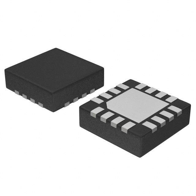
| 产品系列 | isoSPI |
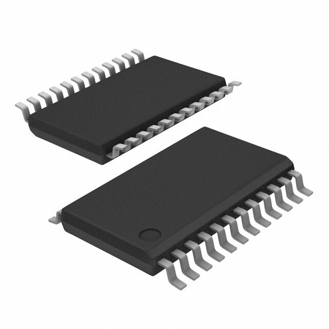
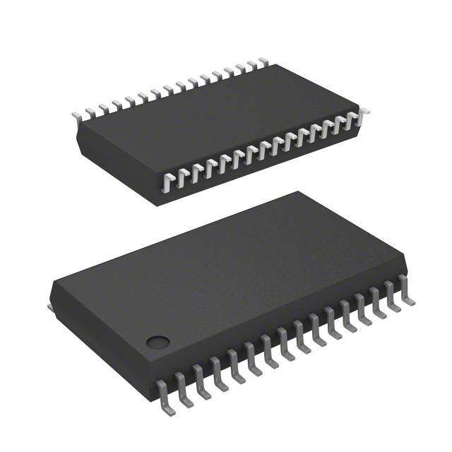
| 供应商器件封装 | 16-MSOP |
| 包装 | 管件 |
| 安装类型 | 表面贴装 |
| 封装/外壳 | 16-TFSOP(0.118",3.00mm 宽) |
| 工作温度 | -40°C ~ 85°C |
| 应用 | 隔离式通信接口 |
| 接口 | SPI |
| 标准包装 | 37 |
| 电压-电源 | 2.7 V ~ 5.5 V |
| 电压-隔离 | - |
| 类型 | 发射器 |
| 输入类型 | SPI |


- 商务部:美国ITC正式对集成电路等产品启动337调查
- 曝三星4nm工艺存在良率问题 高通将骁龙8 Gen1或转产台积电
- 太阳诱电将投资9.5亿元在常州建新厂生产MLCC 预计2023年完工
- 英特尔发布欧洲新工厂建设计划 深化IDM 2.0 战略
- 台积电先进制程称霸业界 有大客户加持明年业绩稳了
- 达到5530亿美元!SIA预计今年全球半导体销售额将创下新高
- 英特尔拟将自动驾驶子公司Mobileye上市 估值或超500亿美元
- 三星加码芯片和SET,合并消费电子和移动部门,撤换高东真等 CEO
- 三星电子宣布重大人事变动 还合并消费电子和移动部门
- 海关总署:前11个月进口集成电路产品价值2.52万亿元 增长14.8%


PDF Datasheet 数据手册内容提取
LTC6820 isoSPI Isolated Communications Interface FEATURES DESCRIPTION n 1Mbps Isolated SPI Data Communications The LTC®6820 provides bidirectional SPI communications n Simple Galvanic Isolation Using Standard between two isolated devices through a single twisted- Transformers pair connection. Each LTC6820 encodes logic states into n Bidirectional Interface Over a Single Twisted Pair signals that are transmitted across an isolation barrier to n Supports Cable Lengths Up to 100 Meters another LTC6820. The receiving LTC6820 decodes the n Very Low EMI Susceptibility and Emissions transmission and drives the slave bus to the appropriate n Configurable for High Noise Immunity or Low Power logic states. The isolation barrier can be bridged by a simple n Engineered for ISO26262 Compliant Systems pulse transformer to achieve hundreds of volts of isolation. n Requires No Software Changes in Most SPI Systems The LTC6820 drives differential signals using matched n Ultralow, 2µA Idle Current source and sink currents, eliminating the requirement n Automatic Wake-Up Detection for a transformer center tap and reducing EMI. Precision n Operating Temperature Range: –40°C to 125°C window comparators in the receiver detect the differential n 2.7V to 5.5V Power Supply signals. The drive currents and the comparator thresholds n Interfaces to All Logic from 1.7V to 5.5V are set by a simple external resistor divider, allowing the n Available in 16-Lead QFN and MSOP Packages system to be optimized for required cable lengths and desired signal-to-noise performance. APPLICATIONS L, LT, LTC, LTM, Linear Technology and the Linear logo are registered trademarks and isoSPI is a trademark of Linear Technology Corporation. All other trademarks are the property of their n Industrial Networking respective owners. Protected by U.S. patents, including 8908779. n Battery Monitoring Systems n Remote Sensors TYPICAL APPLICATION Microcontroller to SPI Slave Isolated Interface Data Rate vs Cable Length 1.2 MASTER CAT-5 ASSUMED µC LTC6820 MSTR 1.0 SDO MOSI IP SDI MISO 120Ω ps) 0.8 b SCCKS SCCSK IM TE (M 0.6 A R A T A 0.4 100 METERS D TWISTED PAIR REMOTE 0.2 SLAVE IC LTC6820 MSTR 0 IP SDI MOSI 1 10 100 120Ω CABLE LENGTH (METERS) SDO MISO SCK SCK IM 6820 TA01b 6820 TA01a CS CS 6820fb 1 For more information www.linear.com/LTC6820
LTC6820 ABSOLUTE MAXIMUM RATINGS (Notes 1, 2, 3) Input Supply Voltages (V and V ) to GND ...........6V Specified Temperature Range DD DDS Pin Voltages LTC6820I .............................................–40°C to 85°C SCK, CS, EN ...............–0.3V to V + 0.3V (6V Max) LTC6820H ..........................................–40°C to 125°C DDS IBIAS, SLOW, IP, IM .....–0.3V to V + 0.3V (6V Max) Storage Temperature Range ..................–65°C to 150°C DD All Other Pin Voltages ..............................–0.3V to 6V Lead Temperature (Soldering, 10 sec) Maximum Source/Sink Current MSOP ...............................................................300°C IP, IM .................................................................30mA MOSI, MISO, SCK, CS ........................................20mA Operating Temperature Range LTC6820I .............................................–40°C to 85°C LTC6820H ..........................................–40°C to 125°C PIN CONFIGURATION TOP VIEW EN IBIAS ICMP GND TOP VIEW 16 15 14 13 EN 1 16 IBIAS MOSI 1 12 SLOW MOSI 2 15 ICMP MISO 2 11 MSTR MISO 3 14 GND 17 SCK 4 13 SLOW SCK 3 10 IP CS 5 12 MSTR CS 4 9 IM VDDS 6 11 IP POL 7 10 IM 5 6 7 8 PHA 8 9 VDD DS OL HA DD MS PACKAGE VD P P V 16-LEAD PLASTIC MSOP UD PACKAGE TJMAX = 150°C, θJA = 120°C/W 16-LEAD (3mm × 3mm) PLASTIC QFN TJMAX = 150°C, θJA = 58.7°C/W EXPOSED PAD (PIN 17) PCB CONNECTION TO GND IS OPTIONAL ORDER INFORMATION http://www.linear.com/product/LTC6820#orderinfo LEAD FREE FINISH TAPE AND REEL PART MARKING* PACKAGE DESCRIPTION SPECIFIED TEMPERATURE RANGE LTC6820IUD#PBF LTC6820IUD#TRPBF LGFM 16-Lead (3mm × 3mm) Plastic QFN –40°C to 85°C LTC6820HUD#PBF LTC6820HUD#TRPBF LGFM 16-Lead (3mm × 3mm) Plastic QFN –40°C to 125°C LTC6820IMS#PBF LTC6820IMS#TRPBF 6820 16-Lead Plastic MSOP –40°C to 85°C LTC6820HMS#PBF LTC6820HMS#TRPBF 6820 16-Lead Plastic MSOP –40°C to 125°C Consult LTC Marketing for parts specified with wider operating temperature ranges. *The temperature grade is identified by a label on the shipping container. For more information on lead free part marking, go to: http://www.linear.com/leadfree/ For more information on tape and reel specifications, go to: http://www.linear.com/tapeandreel/. Some packages are available in 500 unit reels through designated sales channels with #TRMPBF suffix. 6820fb 2 For more information www.linear.com/LTC6820
LTC6820 ELECTRICAL CHARACTERISTICS The l denotes the specifications which apply over the full specified temperature range, otherwise specifications are at T = 25°C. V = 2.7V to 5.5V, V = 1.7V to 5.5V, R = 2k to 20k unless A DD DDS BIAS otherwise specified. All voltages are with respect to GND. SYMBOL PARAMETER CONDITIONS MIN TYP MAX UNITS Power Supply V Operating Supply Voltage Range l 2.7 5.5 V DD V IO Supply Voltage Range (Level Shifting) Affects CS, SCK, MOSI, MISO and EN Pins l 1.7 5.5 V DDS I Supply Current, READY/ACTIVE States R = 2kΩ (I = 1mA) 1/t = 0MHz l 4 4.8 5.8 mA DD BIAS B CLK (Note 4) 1/t = 1MHz 7 mA CLK R = 20kΩ (I = 0.1mA) 1/t = 0MHz l 1.3 2 2.9 mA BIAS B CLK 1/t = 1MHz 2.4 mA CLK Supply Current, IDLE State MSTR = 0V l 2 6 µA MSTR = V l 1 3 µA DD I IO Supply Current (Note 5) SPI Inputs and EN Pin at 0V or V , l 1 µA DDS DDS SPI Outputs Unloaded Biasing V Voltage on IBIAS Pin READY/ACTIVE State l 1.9 2.0 2.1 V BIAS IDLE State 0 V I Isolated Interface Bias Current (Note 6) R = 2k to 20k l V /R mA B BIAS BIAS BIAS A Isolated Interface Current Gain V ≤ 1.6V I = 1mA l 18 20 22 mA/mA IB A B I = 0.1mA l 18 20 24 mA/mA B V Transmitter Pulse Amplitude V = |V – V | V < 3.3V l V – 1.7V V A A IP IM DD DD V ≥ 3.3V l 1.6 V DD V Threshold-Setting Voltage on ICMP Pin V = A • V l 0.2 1.5 V ICMP TCMP TCMP ICMP I Leakage Current on ICMP Pin V = 0V to V l ±1 µA LEAK(ICMP) ICMP DD I Leakage Current on IP and IM Pins IDLE State, V = V = 0V to V l ±2 µA LEAK(IP/IM) IP IM DD A Receiver Comparator Threshold Voltage V = V /2 to V – 0.2V, l 0.4 0.5 0.6 V/V TCMP CM DD DD Gain V = 0.2V to 1.5V ICMP V Receiver Common Mode Bias IP/IM Not Driving (V – V /3 – 167mV) V CM DD ICMP R Receiver Input Resistance Single-Ended to IP or IM l 26 35 42 kΩ IN Idle/Wake-Up (See Figures 13, 14, 15) V Differential Wake-Up Voltage t = 240ns l 240 mV WAKE DWELL (See Figure 13) t Dwell Time at V V = 240mV l 240 ns DWELL WAKE WAKE t Start-Up Time After Wake Detection l 8 µs READY t Idle Time-Out Duration l 4 5.7 7.5 ms IDLE Digital I/O V Digital Voltage Input High, Configuration V = 2.7V to 5.5V (POL, PHA, MSTR, SLOW) l 0.7 • V V IH(CFG) DD DD Pins (PHA, POL, MSTR, SLOW) V Digital Voltage Input Low, Configuration V = 2.7V to 5.5V (POL, PHA, MSTR, SLOW) l 0.3 • V V IL(CFG) DD DD Pins (PHA, POL, MSTR, SLOW) V Digital Voltage Input High, SPI Pins V = 2.7V to 5.5V l 0.7 • V V IH(SPI) DDS DDS (CS, SCK, MOSI, MISO) V = 1.7V to 2.7V l 0.8 • V V DDS DDS V Digital Voltage Input Low, SPI Pins V = 2.7V to 5.5V l 0.3 • V V IL(SPI) DDS DDS (CS, SCK, MOSI, MISO) V = 1.7V to 2.7V l 0.2 • V V DDS DDS V Digital Voltage Input High, EN Pin V = 2.7V to 5.5V l 2 V IH(EN) DDS V = 1.7V to 2.7V l 0.85 • V V DDS DDS V Digital Voltage Input Low, EN Pin V = 2.7V to 5.5V l 0.8 V IL(EN) DDS V = 1.7V to 2.7V l 0.25 • V V DDS DDS V Digital Voltage Output High (CS and SCK) V = 3.3V, Sourcing 2mA l V – 0.2 V OH DDS DDS V = 1.7V, Sourcing 1mA l V – 0.25 V DDS DDS V Digital Voltage Output Low V = 3.3V, Sinking 3.3mA l 0.2 V OL DDS (MOSI, MISO, CS, SCK) V = 1.7V, Sinking 1mA l 0.2 V DDS 6820fb 3 For more information www.linear.com/LTC6820
LTC6820 ELECTRICAL CHARACTERISTICS The l denotes the specifications which apply over the full specified junction temperature range, otherwise specifications are at T = 25°C. V = 2.7V to 5.5V, V = 1.7V to 5.5V, R = 2k to 20k A DD DDS BIAS unless otherwise specified. All voltages are with respect to GND. SYMBOL PARAMETER CONDITIONS MIN TYP MAX UNITS I Digital Pin Input Leakage Current PHA, POL, MSTR, SLOW = 0V to V l ±1 µA LEAK(DIG) DD CS, SCK, MOSI, MISO, EN = 0V to V DDS C Input/Output Pin Capacitance (Note 9) 10 pF I/O Isolated Pulse Timing (See Figure 2) t Chip-Select Half-Pulse Width l 120 150 180 ns 1/2PW(CS) t Chip-Select Pulse Inversion Delay l 200 ns INV(CS) t Chip-Select Response Delay l 140 190 ns DEL(CS) t Data Half-Pulse Width l 40 50 60 ns ½PW(D) t Data Pulse Inversion Delay l 70 ns INV(D) t Data Response Delay (Note 8) l 75 120 ns DEL(D) isoSPI™ Timing—Master (See Figures 3, 4) t SCK Latching Edge to SCK Latching Edge (Note 7) SLOW = 0 l 1 µs CLK SLOW = 1 l 5 µs t MOSI Setup Time Before SCK Latching Edge (Note 8) l 25 ns 1 t MOSI Hold Time After SCK Latching Edge l 25 ns 2 t SCK Low t = t + t ≥ 1µs l 50 ns 3 CLK 3 4 t SCK High t = t + t ≥ 1µs l 50 ns 4 CLK 3 4 t CS Rising Edge to CS Falling Edge l 0.6 µs 5 t SCK Latching Edge to CS Rising Edge (Note 7) l 1 µs 6 t CS Falling Edge to SCK Latch Edge (Note 7) l 1 µs 7 t SCK Non-Latch Edge to MISO Valid (Note 8) l 55 ns 8 t SCK Latching Edge to Short ±1 Transmit l 50 ns 9 t CS Transition to Long ±1 Transmit l 55 ns 10 t CS Rising Edge to MISO Rising (Note 8) l 55 ns 11 isoSPI Timing—Slave (See Figures 3, 4) t isoSPI Data Recognized to SCK (Note 8) SLOW = 0 l 110 145 185 ns 12 Latching Edge SLOW = 1 l 0.9 1.1 1.4 µs t SCK Pulse Width SLOW = 0 l 90 115 150 ns 13 SLOW = 1 l 0.9 1.1 1.4 µs t SCK Non-Latch Edge to isoSPI Data Transmit (Note 8) SLOW = 0 l 115 145 190 ns 14 SLOW = 1 l 0.9 1.1 1.4 µs t CS Falling Edge to SCK Non-Latch Edge PHA = 1 SLOW = 0 l 90 120 160 ns 15 SLOW = 1 l 0.9 1.1 1.4 µs t CS Falling Edge to isoSPI Data Transmit SLOW = 0 l 200 265 345 ns 16 SLOW = 1 l 1.8 2.2 2.8 µs t CS Rising Edge to SCK Latching Edge PHA = 1 SLOW = 0 l 90 120 160 ns 17 SLOW = 1 l 0.9 1.1 1.4 µs t CS Rising Edge to MOSI Rising Edge (Note 8) l 35 ns 18 t Data Return Delay SLOW = 0 l 485 625 ns RTN SLOW = 1 l 3.3 4 µs Note 1: Stresses beyond those listed under Absolute Maximum Ratings Note 3: The LTC6820I is guaranteed to meet specified performance may cause permanent damage to the device. Exposure to any Absolute from –40°C to 85°C. The LTC6820H is guaranteed to meet specified Maximum Rating condition for extended periods may affect device performance from –40°C to 125°C. reliability and lifetime. Note 4: Active supply current (I ) is dependent on the amount of time DD Note 2: All currents into pins are positive, and all voltages are referenced that the output drivers are active on IP and IM. During those times I will DD to GND unless otherwise specified. increase by the 20 • I drive current. For the maximum data rate 1MHz, B the drivers are active approximately 10% of the time if MSTR = 1, and 5% 6820fb 4 For more information www.linear.com/LTC6820
LTC6820 ELECTRICAL CHARACTERISTICS of the time if MSTR = 0. See Applications Information section for more corresponds to 10m of CAT-5 cable (which has a velocity of propagation of detailed information. 66% the speed of light). Use of longer cables would require derating these Note 5: The IO supply pin, V , provides power for the SPI inputs and specs by the amount of additional delay. DDS outputs, including the EN pin. If the inputs are near 0V or V (to avoid Note 8: These specifications do not include rise or fall time. While fall DDS static current in input buffers) and the outputs are not sourcing current, time (typically 5ns due to the internal pull-down transistor) is not a then I includes only leakage current. concern, rising-edge transition time t is dependent on the pull-up DDS RISE Note 6: The LTC6820 is guaranteed to meet specifications with RBIAS resistance and load capacitance. In particular, t12 and t14 require tRISE resistor values ranging from 2k to 20k, with 1% or better tolerance. Those < 110ns (if SLOW = 0) for the slave’s setup and hold times. Therefore, resistor values correspond to a typical I that can range from 0.1mA the recommended time constant is 50ns or less. For example, if the B (for 20k) to 1mA (for 2k). total capacitance on the data pin is 25pF (including self capacitance C of 10pF), the required pull-up resistor value is R ≤ 2kΩ. If these Note 7: These timing specifications are dependent on the delay through I/O PU requirements can’t be met, use SLOW = 1. the cable, and include allowances for 50ns of delay each direction. 50ns Note 9: Guaranteed by design. Not tested in production. TYPICAL PERFORMANCE CHARACTERISTICS V = V , unless otherwise noted. DD DDS Input Voltage Threshold Supply Current (READY/ACTIVE) Supply Current (READY) (Except EN Pin) vs Clock Frequency vs Temperature vs Supply Voltage (V or V ) DD DDS 7 5.3 4.0 IB = 1mA A) 6 VDD = 5V, IB = 1mA VDD = 3V, IB = 1mA A) 5.2 LD (V) 33..50 SPOIN PLIYNS HIGH CURRENT (m 45 CURRENT (m 5.1 VDD =V 5DVD = 3V GE THRESHO 22..05 VIH LOW SUPPLY 3 VDD = 5V, IB = 0.1mA SUPPLY 5.0 UT VOLTA 11..05 2 VDD = 3V, IB = 0.1mA 4.9 INP 0.5 VIL MSTR = 1 1 4.8 0 0 200 400 600 800 1000 –50 –25 0 25 50 75 100 125 1.5 2.0 2.5 3.0 3.5 4.0 4.5 5.0 5.5 FREQUENCY (kHz) TEMPERATURE (°C) SUPPLY VOLTAGE (V) 6820 G01 6820 G02 6820 G03 Supply Current (IDLE) Supply Current (IDLE) Output Resistance vs Supply vs Supply Voltage vs Temperature Voltage (V /V ) OH OL 3.0 3.0 100 VDD = 5V 2.5 2.5 80 URRENT (µA) 12..50 SLAVE (MSTR = 0) URRENT (µA) 21..05 SLAVE (MSTR = 0) SISTANCE (Ω) 60 OSOUUTPRUCTIN G 2mA CURRENT PPLY C 1.0 MASTER (MSTR = 1) PPLY C 1.0 PUT RE 40 U U T S S U MASTER (MSTR = 1) O 20 0.5 0.5 OUTPUT SINKING 3.3mA CURRENT 0 0 0 2.5 3.0 3.5 4.0 4.5 5.0 5.5 –50 –25 0 25 50 75 100 125 1.5 2.5 3.5 4.5 5.5 SUPPLY VOLTAGE (V) TEMPERATURE (°C) SUPPLY VOLTAGE (V) 6820 G04 6820 G05 6820 G19 6820fb 5 For more information www.linear.com/LTC6820
LTC6820 TYPICAL PERFORMANCE CHARACTERISTICS V = V , unless otherwise noted. DD DDS IBIAS Voltage vs Temperature IBIAS Voltage Load Regulation IBIAS Voltage vs Supply Voltage 2.04 2.010 2.010 VDD = 3V VDD = 3V 3 PARTS N VOLTAGE (V) 22..0002 N VOLTAGE (V)22..000005 N VOLTAGE (V)22..000050 IBIB = = 0 1.1mmAA IBIAS PI 1.98 IBIAS PI1.995 IBIAS PI1.995 IB = 1mA IB = 0.1mA 1.96 1.990 1.990 –50 –25 0 25 50 75 100 125 0 0.2 0.4 0.6 0.8 1.0 2.5 3 3.5 4 4.5 5 5.5 TEMPERATURE (°C) IBIAS CURRENT (mA) SUPPLY VOLTAGE (V) 6820 G07 6820 G08 6820 G09 Driver Current Gain Driver Current Gain Driver Current Gain vs Amplitude vs IBIAS Current (I ) vs Supply Voltage B 23 22.0 22.0 VA(MAX) = 1.6V VA = 1V VA = 1V 22 VDD = 5V FOR VDD > 3.3V 21.5 21.5 N A (mA/mA)IB 2201 IB = 1mA IBV D=D 0 =.1 5mVA AIN (mA/mA)222010...005 VVDDDD == 53VV AIN (mA/mA)222010...005 IB = 0.1mAIB = 1mA GAI T G T G URRENT 19 IBV D=D 0 =.1 3mVA VIBD =D 1=m 3AV CURREN1199..05 CURREN1199..50 C 18 VA(MAX) = 1.3V 18.5 18.5 FOR VDD = 3V 17 18.0 18.0 0 0.5 1.0 1.5 2.0 0 0.2 0.4 0.6 0.8 1.0 2.5 3 3.5 4 4.5 5 5.5 PULSE AMPLITUDE VA (V) IBIAS CURRENT (mA) SUPPLY VOLTAGE (V) 6820 G10 6820 G11 6820 G12 Driver Current Gain Driver Common Mode Voltage Driver Common Mode Voltage vs Temperature vs Temperature vs Pulse Amplitude 22.0 5 5.0 VA = 1V VA = 1V 21.5 IB = 0.1mA, VDD = 5V 4.5 IB = 0.1mA, VDD = 5V A/mA)21.0 IB = 0.1mA, VDIBD == 15mVA, VDD = 5V ODE (V) 4 IB = 1mA, VDD = 5V ODE (V) 4.0 IB = 1mA, VDD = 5V m20.5 M 3 M 3.5 RENT GAIN (2109..05 IB = 0.1mA,I BV D= D1 m= A3V, VDD = 3V R COMMON 2 IB = 0.1mA, VDD = 3V R COMMON 32..05 IB = 0.1mA, VDD = 3V CUR19.0 RIVE IB = 1mA, VDD = 3V RIVE 2.0 D 1 D 18.5 1.5 IB = 1mA, VDD = 3V 18.0 0 1.0 –50 –25 0 25 50 75 100 125 –50 –25 0 25 50 75 100 125 0 0.5 1.0 1.5 2.0 TEMPERATURE (°C) TEMPERATURE (°C) PULSE AMPLITUDE (V) 6820 G13 6820 G14 6820 G15 6820fb 6 For more information www.linear.com/LTC6820
LTC6820 TYPICAL PERFORMANCE CHARACTERISTICS V = V , unless otherwise noted. DD DDS Comparator Threshold Gain Comparator Threshold Gain Comparator Threshold Gain vs ICMP Voltage vs Common Mode vs Temperature 0.56 0.56 0.56 3 PARTS VDD = 3V MPARATOR THRESHOLD GAIN (V/V) 00000.....5554420486 MPARATOR THRESHLD GAIN (V/V)00000.....5554420486 VVVIICVCDMMDDPD P= = ==3 1V30VV.2V VVVICIDVCMDMDP DP= = ==5 1 V50VV.2V MPARATOR THRESHLD GAIN (V/V) 00000.....5554420486 3 PARTS CO VDD = 3V CO CO VICMP = 1V VDD = 5V VICMP = 0.2V 0.44 0.44 0.44 0 0.2 0.4 0.6 0.8 1.0 1.2 1.4 1.6 1.5 2.0 2.5 3.0 3.5 4.0 4.5 5.0 5.5 –50 –25 0 25 50 75 100 125 ICMP VOLTAGE (V) COMMON MODE VOLTAGE (V) TEMPERATURE (°C) 6820 G16 6820 G17 6820 G18 Wake-Up Pulse Amplitude vs Dwell Time Start-Up Time 300 V) VDD = 3V m (WAKE250 WAGKUEA-RUAPN RTEEGEIDON 5V/DCISV 3.6µs V E, UD 200 IBIAS LIT 2V/DIV P M A E 150 S L IP-IM U P 1V/DIV P U 100 E- K A W 50 VDDS = 5V 1µs/DIV 6820 G06 0 150 300 450 600 MSTR = 1 WAKE-UP DWELL TIME, tDWELL (ns) RBIAS = 2k 6820 G20 SPI Signal and isoSPI Pulses, MSTR = 1 SPI Signal and isoSPI Pulses, MSTR = 0 IP-IM CS 2V/DIV 5V/DIV SCK CS 5V/DIV 5V/DIV MOSI SCK 5V/DIV 5V/DIV MIS0 MOSI 5V/DIV 5V/DIV IP-IM MIS0 2V/DIV 5V/DIV VDD = 5V 1.2µs/DIV 6820 G21 VDD = 5V 1.2µs/DIV 6820 G22 VDDS = 3.3V VDDS = 5V PHA = 1 PHA = 0 POL = 1 POL = 0 6820fb 7 For more information www.linear.com/LTC6820
LTC6820 PIN FUNCTIONS (QFN/MSOP) MOSI (Pin 1/Pin 2): SPI Master Out/Slave In Data. If V (Pin 8/Pin 9): Device Power Supply Input. Connect DD connected on the master side of a SPI interface (MSTR a bypass capacitor of at least 0.01μF directly between pin high), this pin receives the data signal output from V and GND. DD the master SPI controller. If connected on the slave side IM (Pin 9/Pin 10): Isolated Interface Minus Input/Output. of the interface (MSTR pin low), this pin drives the data signal input to the slave SPI device. The output is open IP (Pin 10/Pin 11): Isolated Interface Plus Input/Output. drain, so an external pull-up resistor to V is required. DDS MSTR (Pin 11/Pin 12): Serial Interface Master/Slave MISO (Pin 2/Pin 3): SPI Master In/Slave Out Data. If con- Selector Input. Tie this pin to VDD if the device is on the nected on the master side of a SPI interface (MSTR pin master side of the isolated interface. Tie this pin to GND high), this pin drives the data signal input to the master SPI if the device is on the slave side of the isolated interface. controller. If connected on the slave side of the interface SLOW (Pin 12/Pin 13): Slow Interface Selection Input. For (MSTR pin low), this pin receives the data signal output clock frequencies at or below 200kHz, or if slave devices from the slave SPI device. The output is open drain, so cannot meet timing requirements, this pin should be tied an external pull-up resistor to V is required. DDS to V . For clock frequencies above 200kHz, this pin DD SCK (Pin 3/Pin 4): SPI Clock Input/Output. If connected on should be tied to GND. the master side of the interface (MSTR pin high), this pin GND (Pin 13/Pin 14): Device Ground. receives the clock signal from the master SPI controller. ICMP (Pin 14/Pin 15): Isolated Interface Comparator This input should not be pulled above V . If connected DDS Voltage Threshold Set. Tie this pin to the resistor divider on the slave side of the interface (MSTR pin low), this pin between IBIAS and GND to set the voltage threshold of the outputs the clock signal to the slave device. The output interface receiver comparators. The comparator thresholds driver is push-pull; no external pull-up resistor is needed. are set to 1/2 the voltage on the ICMP pin. CS (Pin 4/Pin 5): SPI Chip Select Input/Output. If connected IBIAS (Pin 15/Pin 16): Isolated Interface Current Bias. on the master side of the interface (MSTR pin high), this Tie IBIAS to GND through a resistor divider to set the pin receives the chip select signal from the master SPI interface output current level. When the device is enabled, controller. This input should not be pulled above V . If DDS this pin is approximately 2V. When transmitting pulses, connected on the slave side of the interface (MSTR pin the sink current on each of the IP and IM pins is set to low), this pin outputs the chip select signal to the slave 20 times the current sourced from pin IBIAS to GND. device. The output driver is push-pull; no external pull-up Limit the capacitance on the IBIAS pin to less than 50pF resistor is needed. to maintain the stability of the feedback circuit regulating V (Pin 5/Pin 6): SPI Input/Output Power Supply Input. DDS the IBIAS voltage. The output drivers for the SCK and CS pins use the V DDS EN (Pin 16/Pin 1): Device Enable Input. If high, this pin input as their positive power supply. The input threshold forces the LTC6820 to stay enabled, overriding the internal voltages of SCK, CS, MOSI, MISO and EN are determined IDLE mode function. If low, the LTC6820 will go into IDLE by V . May be tied to V or to a supply above or below DDS DD mode after the CS pin has been high for 5.7ms (when V to level shift the SPI I/O. If separate from V , con- DD DD MSTR pin is high) or after no signal on the IP/IM pins for nect a bypass capacitor of at least 0.01μF directly between 5.7ms (when MSTR pin is low). The LTC6820 will wake-up V and GND. DDS less than 8µs after CS falls (MSTR high) or after a signal POL (Pin 6/Pin 7): SPI Clock Polarity Input. Tie to V or DD is detected on IP/IM (MSTR low). GND. See Operation section for details. Exposed Pad (Pin 17, QFN Package Only): Exposed pad PHA (Pin 7/Pin 8): SPI Clock Phase Input. Tie to V or DD may be left open or connected to device GND. GND. See Operation section for details. 6820fb 8 For more information www.linear.com/LTC6820
LTC6820 BLOCK DIAGRAM TS EN VDD VDD TION INPU READCYS IWDALEK ET IDMEETOEUCTT2V IBIAS IB RB1 A ICMP 0.1µF MSTR GUR GIC VDD RBIAS = RB1 + RB2 SLOW NFI LO RB2 POL ED CO VIC3MP+ 167mV +– R OPEN E PHA POW WIHDELNE 35k -D VD 35k VDDS N RPU EVNDDS TRANSLATION E QUALIFICATIO RRxx == +–11 THRESHOL+–D 0.5x (TO MOSI IF MSTR = 0) MOSI PI PIN PULS S (TO MISO IF MSTR = 1) MISO ED ER Tx = +1 IP W SCCSK -PODDS TIMING Tx = –1 IDRV IM RM V GND Tx • 20 • IB 6820 BD OPERATION The LTC6820 creates a bidirectional isolated serial port The receiver consists of a window comparator with a interface (isoSPI) over a single twisted pair of wires, with differential voltage threshold, V . When V – V TCMP IP IM increased safety and noise immunity over a nonisolated is greater than +V , the comparator detects a logic TCMP interface. Using transformers, the LTC6820 translates +1. When V – V is less than –V , the comparator IP IM TCMP standard SPI signals (CS, SCK, MOSI and MISO) into pulses detects a logic –1. A logic 0 (null) indicates V – V is IP IM that can be sent back and forth on twisted-pair cables. between the positive and negative thresholds. A typical system uses two LTC6820 devices. The first is The comparator outputs are sent to pulse timers (filters) paired with a microcontroller or other SPI master. Its IP that discriminate between short and long pulses. and IM transmitter/receiver pins are connected across an isolation barrier to a second LTC6820 that reproduces the Selecting Bias Resistors SPI signals for use by one or more slave devices. The adjustable signal amplitude allows the system to trade The transmitter is a current-regulated differential driver. power consumption for communication robustness, and The voltage amplitude is determined by the drive current the adjustable comparator threshold allows the system to and the equivalent resistive load (cable characteristic account for signal losses. impedance and termination resistor, R ). M 6820fb 9 For more information www.linear.com/LTC6820
LTC6820 OPERATION ISOLATION BARRIER MSTR IP IP MSTR MASTER LTC6820 RM RM LTC6820 SLAVE SDO MOSI IM IM MOSI SDI SDI MISO IBIAS TWISTED-PAIR CABLE IBIAS MISO SDO SCK SCK RB1WITH CHARACTERISTIC IMPEDANCE RM RB1 SCK SCK CS CS CS CS ICMP ICMP RB2 RB2 6820 F01 Figure 1. Typical System Using Two LTC6820 Devices The transmitter drive current and comparator voltage isoSPI Pulse Detail threshold are set by a resistor divider (R = R + R ) BIAS B1 B2 The isoSPI transmitter can generate three voltage levels: between the IBIAS pin and GND, with the divided voltage +V , 0V, and –V . To eliminate the DC signal component A A tied to the ICMP pin. When the LTC6820 is enabled (not and enhance reliability, isoSPI pulses are defined as IDLE), I is held at 2V, causing a current, I , to flow BIAS B symmetric pulse pairs. A +1 pulse pair is defined as a out of the IBIAS pin. The IP and IM pin drive currents are +V pulse followed by a –V pulse. A –1 pulse pair is –V A A A 20 • I . The comparator threshold is half the voltage on B followed by +V . A the ICMP pin (V ). ICMP The duration of each pulse is defined as t . (The total 1/2PW As an example, if divider resistor R is 1.21k and resistor B1 isoSPI pulse duration is 2 • t ). The LTC6820 allows 1/2PW R is 787Ω (so that R = 2k), then: B2 BIAS for two different t values so that four types of pulses 1/2PW 2V can be transmitted, as listed in Table 1. I = =1mA B R +R B1 B2 Table 1. isoSPI Pulse Types PULSE TYPE FIRST LEVEL SECOND LEVEL ENDING LEVEL I = I = I = 20 • I = 20mA DRV IP IM B Long +1 +V (150ns) –V (150ns) 0V A A V =2V(cid:127) RB2 =I (cid:127)R =788mV Long –1 –VA (150ns) +VA (150ns) 0V ICMP B B2 RB1+RB2 Short +1 +VA (50ns) –VA (50ns) 0V Short –1 –V (50ns) +V (50ns) 0V A A V = 0.5 • V = 394mV TCMP ICMP Long pulses are used to transmit CS changes. Short pulses In this example, the pulse drive current IDRV will be 20mA, transmit data (MOSI or MISO). An LTC6820 detects four and the receiver comparators will detect pulses with IP-IM types of communication events from the SPI master: CS amplitudes greater than ±394mV. falling, CS rising, SCK latching MOSI = 0, and SCK latch- ing MOSI = 1. It converts each event into one of the four If the isolation barrier uses 1:1 transformers connected pulse types, as shown in Table 2. by a twisted pair and terminated with 100Ω resistors on each end, then the transmitted differential signal amplitude Table 2. Master Communication Events (±) will be: SPI MASTER EVENT TRANSMITTED PULSE R CS Rising Long +1 V =I (cid:127) M =1V A DRV CS Falling Long –1 2 SCK Latching Edge, MOSI = 1 Short +1 (This result ignores transformer and cable losses, which SCK Latching Edge, MOSI = 0 Short –1 will reduce the amplitude). 6820fb 10 For more information www.linear.com/LTC6820
LTC6820 OPERATION On the other side of the isolation barrier (i.e., the other end Characteristics table, these specifications are further of the cable) another LTC6820 is configured to interface separated into CS (long) and Data (short) parameters. with a SPI slave. It receives the transmitted pulses and A valid pulse must meet the minimum spec for t and 1/2PW reconstructs the SPI signals on its output port, as shown the maximum spec for t . In other words, the half-pulse INV in Table 3. In addition, the slave device may transmit a width must be long enough to pass through the appropriate return data pulse to the master to set the state of MISO. pulse timer, but short enough for the inversion to begin See isoSPI Interaction and Timing for additional details. within the valid window of time. Table 3. Slave SPI Port Output The response observed at MOSI, MISO or CS will occur RECEIVED PULSE SPI PORT ACTION RETURN PULSE after delay t from the pulse inversion. DEL Long +1 Drive CS High None Long –1 Drive CS Low Setting Clock Phase and Polarity (PHA and POL) Short –1 Pulse Short +1 1. Set MOSI = 1 if MISO = 0 SPI devices often use one clock edge to latch data and 2. Pulse SCK (No Return Pulse the other edge to shift data. This avoids timing problems Short –1 1. Set MOSI = 0 if MISO = 1) 2. Pulse SCK associated with clock skew. There is no standard to specify whether the shift or latch occurs first. There is also no A slave LTC6820 never transmits long (CS) pulses. Fur- requirement for data to be latched on a rising or falling thermore, a slave will only transmit a short –1 pulse (when clock edge, although latching on the rising edge is most MISO = 0), never a +1 pulse. This allows for multiple slave common. The LTC6820 supports all four SPI operating devices on a single cable without risk of collisions (see modes, as configured by the PHA and POL Pins. Multidrop section). Table 4. SPI Modes isoSPI Pulse Specifications MODE POL PHA DESCRIPTION Figure 2 details the timing specifications for the +1 and 0 0 0 SCK Idles Low, Latches on Rising (1st) Edge –1 isoSPI pulses. The same timing specifications apply to 1 0 1 SCK Idles Low, Latches on Falling (2nd) Edge either version of these symmetric pulses. In the Electrical 2 1 0 SCK Idles High, Latches on Falling (1st) Edge 3 1 1 SCK Idles High, Latches on Rising (2nd) Edge +1 PULSE VA VTCMP t1/2PW VIP – VIM t1/2PW –VTCMP tINV –VA tDEL MOSI, MISO OR CS –1 PULSE VA tINV VTCMP t1/2PW VIP – VIM t1/2PW –VTCMP tDEL –VA MOSI, MISO OR CS 6820 F02 Figure 2. isoSPI Differential Pulse Detail 6820fb 11 For more information www.linear.com/LTC6820
LTC6820 OPERATION If POL = 0, SCK idles low. Data is latched on the rising isoSPI data pulse (M , M , … M ) while simultaneously N N–1 0 (first) clock edge if PHA = 0 and on the falling (second) latching the slave’s data bit. As the slave LTC6820 receives clock edge if PHA = 1. each data bit it will set the slave MOSI pin to the proper state and then generate an SCK pulse before returning the If POL =1, SCK idles high. Data is latched on the falling slave’s MISO data (either as a Short –1 pulse, or as a null). (first) clock edge if PHA = 0 and on the rising (second) clock edge if PHA = 1. At the end of communication, the final data bit sent by the slave (either as a pulse or null) will be ignored by The two most common configurations are mode 0 (PHA = 0 the master controller. (The slave LTC6820 must return a and POL = 0) and mode 3 (PHA = 1 and POL = 1) because data bit since it cannot predict when communications will these modes latch data on a rising clock edge. cease.) The master SPI device can then raise CS, which is transmitted to the slave in the form of a Long +1 pulse. isoSPI Interaction and Timing The process ends with the slave LTC6820 transitioning The timing diagrams in Figures 3 and 4 show how an iso- CS high, and returning SCK to the idle state if PHA = 1. SPI in master mode (connected to a SPI master) interacts with an isoSPI in slave mode (connected to a SPI slave). Rise Time Figure 3 details operation with PHA = 0 (and shows SCK MOSI and MISO outputs have open-drain drivers. The rise signals for POL = 0 or 1). Figure 4 provides the timing time t for the data output is determined by the pull-up RISE diagram for PHA = 1. Although not shown, it is acceptable resistance and load capacitance. R must be small enough PU to use different SPI modes (PHA and POL settings) on the to provide adequate setup and hold times. master and slave devices. A master SPI device initiates communication by lowering Slow Mode CS. The LTC6820 converts this transition into a Long –1 When configured for slave operation, the LTC6820 provides pulse on its IP/IM pins. The pulse traverses the isolation two operating modes to ensure compatibility with a wide barrier (with an associated cable delay) and arrives at the range of SPI timing scenarios. These modes are referred IP/IM pins of the slave LTC6820. Once validated, the Long to as fast and slow mode, and are set using the SLOW –1 pulse is converted back into a falling CS transition, this pin. When configured for master operation, the SLOW time supplied to the slave SPI device. If slave PHA = 1, pin setting has no effect on the LTC6820 operation. In SCK will also leave the idle state at this time. this case, it is recommended to tie the SLOW pin to GND. Before the master SPI device supplies the first latching In fast mode (SLOW pin tied to GND), the LTC6820 can clock edge (usually a rising edge, but see Table 4 for operate at clock rates up to 1MHz (t = 1µs). However, CLK exceptions), the slave LTC6820 must transmit the initial some SPI slave devices can’t respond quickly enough to slave data bit S , which it determines by sampling the N support this data rate. Fast mode requires a slave to operate state of MISO after a suitable delay. with setup and response times of 100ns, as well as 100ns If MISO = 0, the slave will transmit a Short –1 pulse to the clock widths. In addition, allowances must be made for the master. The master LTC6820 will receive and decode the RC rise time of MOSI and MISO’s open-drain outputs. In pulse and set the master MISO = 0 (matching the slave). slow mode (SLOW pin tied to V+), the timing requirement However, if the slave MISO=1, the slave does not transmit are relaxed at the expense of maximum data rate. As indi- a pulse. The master will interpret this null response as a 1 cated in the Electrical Characteristics, the clock pulses and and set the master MISO = 1. This makes it possible to required setup and response times are increased to 0.9µs connect multiple slave LTC6820’s to a single cable with minimum. Accordingly, the minimum tCLK (controlled by no conflicting signals (see Multidrop section). the master) must be limited to 5µs. The SLOW pin setting has no effect on the master LTC6820 (with MSTR = 1). After the falling CS sequence, every latching clock edge on the master converts the state of the MOSI pin into an 6820fb 12 For more information www.linear.com/LTC6820
LTC6820 OPERATION 5000 6820 F03 0 0 5 1 4 = t5 SB C t18 S) C t11 t10 NORED tDEL( 4000 G I t6 00 5 3 T O S N+1 M0 SLAVE DOETRANSMIT 3000 HA = 0) P N-2 PLE m ( S M A a S gr t14 t13 2500 TIME (ns) ming Dia MN-1 t12 ver Ti tDEL(D) tRISE E 2000 Transcei t3 SN-1 AMPL e 3. S r u D) g tCLK t8 RISE tDEL( tRTN 1500 Fi t t4 N M 2 t 0 t1 100 t9 LE SN MP A S) S C t7 tDEL(t16 00 0 5 = B S t10 C 0 CS L = 0) L = 1) MOSI MISO ISO ISO CS L = 0) L = 1) MOSI MISO O O O O P P P P K ( K ( K ( K ( C C C C S S S S 6820fb 13 For more information www.linear.com/LTC6820
LTC6820 OPERATION 50006820 F04 0 1 t17 450 = t5 SB C 18 t S) C t11 t10 NORED tDEL( 4000 G I t6 NOTT +1 3500 S MI MO SLAVE DOETRANS = 1) 00 A 30 H SN-2 MPLE m (P A a S r g tDEL(D) t14 t13 2500 TIME (ns) ming Dia MN-1 t12 ver Ti t3 SN-1 tDEL(D) tRISE SAMPLE 2000 re 4. Transcei u g tCLK N 500 Fi t8 RISE tRT 1 t t4 N M t2 0 t1 100 t9 LE SN MP A S) S C t7 0 tDEL(t16 t15 500 = B S t10 C 0 CS L = 1) L = 0) MOSI MISO ISO ISO CS L = 1) L = 0) MOSI MISO O O O O P P P P K ( K ( K ( K ( C C C C S S S S 6820fb 14 For more information www.linear.com/LTC6820
LTC6820 OPERATION Figure 6 demonstrates slow mode, as compared to fast VDD VDD mode in Figure 5. +– VIC3MP+ 167mV IP-IM 2V/DIV SCK POS OPEN WHEN IDLE 5V/DIV IP MOSI 35k 5V/DIV RM MISO 35k 5V/DIV IM VDD = 5V 200ns/DIV 6820 F05 NEG POS VDDS = 5V Figure 5. Fast Mode (SLOW = 0) NEG 20 • IB VIP – VIM 6820 F07 IP-IM 2V/DIV Figure 7. Pulse Driver SCK 5V/DIV 25 MOSI SOURCING OUTPUT 5V/DIV MISO mA) 20 5V/DIV T ( N E 1V AMPLITUDE VDD = 5V 1µs/DIV 6820 F06 URR 15 VDDS = 5V NK C SINKING OUTPUT SI 10 Figure 6. Slow Mode (SLOW = 1) E/ C R U O IP and IM Pulse Driver S 5 VDD = 3V IB = 1mA The IP and IM pins transmit and receive the isoSPI pulses. 0 0 0.5 1 1.5 2 2.5 3 The transmitter uses a current-regulated driver (see VIP OR VIM (V) Figure 7) to establish the pulse amplitude, as determined 6820 F08 by the IBIAS pin current, I , and the load resistance. The B Figure 8. Drive Source/Sink vs Output Voltage sinking current source is regulated to 20x the bias current I . B The sourcing current source operates in a current-starved 3.0 (resistive) manner to maintain the sourcing pin’s voltage SOURCING near V , as shown in Figures 8 and 9. The common mode 2.5 OUTPUT DD voltage (while driving) is dependent on bias current and V) E ( 2.0 output amplitude. AG VCM T L O 1.5 V The output driver will regulate the common mode and T U P peak swing of IP and IM to the proper levels, allowing for T 1.0 OU SINKING a broad range of output amplitude with fairly flat gain, as OUTPUT 0.5 shown in Figure 10. VDD = 3V IB = 1mA 0 0 0.5 1 1.5 2 2.5 3 PULSE AMPLITUDE (V) 6820 F09 Figure 9. Output Voltages and Common Mode vs Amplitude 6820fb 15 For more information www.linear.com/LTC6820
LTC6820 OPERATION 25 3.0 TRANSMIT SHORT +1 2.5 20 mA) 2.0 IP IM RENT GAIN (mA/ 1105 VOLTAGE (V) 011...505 IP-IMRECEIVE SHORT –1 R 0 U C 5 –0.5 0 VISD =D 1=m 3AV –1.0 VIBD =D 1=m 3AV –1.5 0 0.5 1 1.5 2 2.5 3 0 200 400 600 800 1000 PULSE AMPLITUDE (V) TIME (ns) 6820 F10 6820 F11 Figure 10. A Current Gain vs Amplitude Figure 11. Transmitting and Receiving Data IB This type of driver does not require a center-tapped transformer, but such a transformer may improve noise IDLE immunity, especially if it has a common mode choke. See IDLE WAKE-UP SIGNAL the Applications Information section for additional details. TIMEOUT (tREADY) (tIDLE) Receiver Common Mode Bias READY NO ACTIVITY When not transmitting, the output driver maintains IP ON isoSPI TRANSMIT/RECEIVE and IM near V with a pair of 35k (R ) resistors to a PORT DD IN voltage of VDD – VICMP/3 – 167mV. This weak bias net- ACTIVE 6820 F12 work holds the outputs near their desired operating point without significantly loading the cable, which allows a large Figure 12. State Diagram number of LTC6820’s to be paralleled without affecting signal amplitude. In the READY state all circuitry is enabled and ready to Figure 11 shows the differential and single-ended IP and transmit or receive, but is not actively transmitting on IP IM signals while transmitting and receiving data. The and IM. driver forces the common mode voltage it needs while transmitting, then it returns to the bias level with a time Supply current increases when actively communicating, constant of R • C /2, where C is the sum of the so this condition is referred to as the ACTIVE state. IN LOAD LOAD capacitance at the IP and IM pins. Supply Current When the LTC6820 is in low power IDLE mode, the bias Table 5 provides equations for estimating I in each state. voltage is disconnected from the 35k resistors, resulting DD The results are for average supply current (as opposed in a 70k differential load. to peak currents), and make the assumption that a slave State Diagram is returning an equal number of 0s and 1s (significant because the slave doesn’t generate +1 data pulses, so the During periods of no communication, a low current IDLE average driver current is smaller). (or shutdown) state is available to reduce power. In the IDLE state the LTC6820 shuts down most of the circuitry. A slave device uses a low current comparator to monitor for activity, so it has larger IDLE current. 6820fb 16 For more information www.linear.com/LTC6820
LTC6820 OPERATION Figure 15 demonstrates a simple procedure for waking Table 5. I Equations DD a master (MSTR = 1) LTC6820 and its connected slave STATE MSTR ESTIMATED I DD (MSTR = 0). A negative edge on CS causes the master IDLE 0 (slave) 2µA to drive IBIAS to 2V and, after a short delay, transmit a 1 (master) 1µA long +1 pulse. (If CS remains low throughout t , the READY 0 or 1 1.7mA + 3 • I READY B LTC6820 would first generate a –1 pulse, then the +1 ACTIVE 0 (slave) 2mA+3+20(cid:127)100tnCsLK(cid:127)0.5 (cid:127)IB pwualksee- uwph esnig CnSal rfeotru rtnhse hsilgavhe). dTehveic leo,n wg hpiuclhs er esseprovensd sa sb ay 1 (master) 100ns driving its IBIAS pin to 2V and entering the READY state. 2mA+3+20(cid:127) tCLK (cid:127)IB IDLE Mode and Wake-Up Detection 240mV IP IPAC To conserve power, an LTC6820 in slave mode (MSTR = 0) 240ns DELAY |IPAC–IMAC| > 240mV (FILTER) will enter an IDLE state after 5.7ms (t ) of inactivity IDLE on the IP/IM pins. In this condition I is reduced to less 240ns IM IMAC SLAVE DD MASTER than 6µA and the SPI pins are idled (CS = 1, MOSI = 1 CS and SCK = POL). WAKE-UP The LTC6820 will continue monitoring the IP and IM IDLE TIMER pins using a low power AC-coupled detector. It will wake up when it sees a differential signal of 240mV or greater EN tREADY READY tIDLE (IBIAS = 2V) that persists for 240ns or longer. In practice, a long (CS) 6820 F13 isoSPI pulse is sufficient to wake the device up. Once the Figure 13. Wake-Up Detection and IDLE Timer comparator generates the wake-up signal it can take up to 8µs (t ) for bias circuits to stabilize. READY REJECTS Figure 14 details the sequence of waking up a slave LTC6820 COMMON MODE NOISE (placing it in the READY state), using it to communicate, IP then allowing it to return to the low power IDLE state. IM A LTC6820 in master mode (MSTR = 1) doesn’t use the IP-IM tDWELL tIDLE wake-up detection comparator. A falling edge on CS will READY tREADY OK TO COMMUNICATE 6820 F14 enable the isoSPI port within t , and the LTC6820 READY Figure 14. Slave LTC6820 Wake-Up/Idle Timing will transmit a long (CS) pulse as it leaves the IDLE state. (The polarity of the pulse matches the CS state at the end of tREADY). ALLOW >2 • tREADY TO WAKE MASTER AND SLAVE The master LTC6820 will remain in the READY/ACTIVE MASTER CS tREADY tIDLE state as long as CS = 0. If CS transitions high and EN = 0 MASTER IBIAS it will enter the IDLE state, but not until t expires. IDLE IP-IM This prevents the device from shutting down between tDWELL tREADY tIDLE SLAVE data packets. IBIAS SLAVE CS In either master or slave mode the IDLE feature may be 6820 F15 disabled by driving EN high. This forces the device to Figure 15. Master and Slave Wake-Up/Idle Sequence remain “ready” at all times. 6820fb 17 For more information www.linear.com/LTC6820
LTC6820 OPERATION Multidrop n The SPI slaves must be addressable, because they will all see the same CS signal (as decoded by each slave Multiple slaves can be connected to a single master by con- LTC6820). necting them in parallel (multidrop configuration)along one cable. As shown in Figure 16, the cable should be terminated n When not addressed, the slave SDO must remain high. only at the beginning (master) and the end. In between, the When a slave is not addressed, its LTC6820 will not trans- additional LTC6820’s and their associated slave devices will mit data pulses as long as MISO (the SPI device’s SDO) be connected to “stubs” on the cable. These stubs should remains high. This eliminates the possibility for collisions, be kept short, with as little capacitance as possible, to avoid as only the addressed slave device will ever be returning degrading the termination along the cable. data to the master. The multidrop scheme is only possible if the SPI slaves have certain characteristics: MASTER LTC6820 LTC6820 SLAVE 1 MSTR MSTR SDO MOSI IP IP MOSI 1 SDI SDI MISO RM MISO SDO SCK SCK IM IM SCK SCK CS CS CS CS 1 1 LTC6820 SLAVE 2 MSTR IP 2 MOSI SDI MISO SDO IM SCK SCK CS CS 2 2 LTC6820 SLAVE 3 MSTR IP 3 MOSI SDI RM MISO SDO IM SCK SCK CS CS 3 3 6820 F16 Figure 16. Multidropping Multiple Slaves on a Single Cable 6820fb 18 For more information www.linear.com/LTC6820
LTC6820 APPLICATIONS INFORMATION isoSPI Setup For cables over 50 meters: The LTC6820 allows each application to be optimized for I = 1mA B power consumption or for noise immunity. The power V = (20 • I ) • (R /2) A B M and noise immunity of an isoSPI system is determined by the programmed IB current. The IB current can range VTCMP = 1/4 • VA from 0.1mA to 1mA. A low I reduces the isoSPI power B V = 2 • V ICMP TCMP consumption in the READY and ACTIVE states, while a R = V /I high I increases the amplitude of the differential signal B2 ICMP B B voltage V across the matching termination resistor, R . A M 2V RB1= –RB2 IB is programmed by the sum of the RB1 and RB2 resis- IB tors connected between the I pin and GND. For most BIAS applications setting I to 0.5mA is a good compromise The maximum data rate of an isoSPI link is determined by B between power consumption and noise immunity. Using the length of the cable used. For cables 10 meters or less this I setting with a 1:1 transformer and R = 120Ω, R the maximum 1MHz SPI clock frequency is possible. As B M B1 should be set to 2.8k and R set to 1.2k. In a typical CAT5 the length of the cable increases the maximum possible B2 twisted pair these settings will allow for communication SPI clock rate decreases. This is a result of the increased up to 50m. propagation delays through the cable creating possible timing violations. For applications that require cables longer than 50m it is recommended to increase the amplitude V by increasing Cable delay affects three timing specifications, t , t , and A CLK 6 I to 1mA. This compensates for the increased insertion t . In the Electrical Characteristics table, each is derated by B 7 loss in the cable and maintains high noise immunity. So 100ns to allow for 50ns of cable delay. For longer cables, when using cables over 50m and, again, using a trans- the minimum timing parameters may be calculated as former with a 1:1 turns ratio and R = 120Ω, R would shown below: M B1 be 1.4k and R would be 600Ω. B2 t , t , and t > 0.9µs + 2 • t CLK 6 7 CABLE Other I settings can be used to reduce power consumption B or increase the noise immunity as required by the applica- Pull-Up Resistance Considerations tion. In these cases when setting V and choosing R ICMP B1 The data output (MOSI if MSTR = 0, MISO if MSTR = and R resistor values the following rules should be used: B2 1) requires a pull-up resistor, R . The rise time t is PU RISE For cables 50 meters or less: determined by RPU and the capacitance on the pin. RPU must be small enough to provide adequate setup and hold I = 0.5mA B times. For a slave device, the time constant must be less V = (20 • I ) • (R /2) than t and t . In fast mode, 50ns is recommended. A B M 12 14 V = 1/2 • V R < 50ns/C TCMP A PU LOAD V = 2 • V Larger pull-up resistances, up to 5k, can be used in slow ICMP TCMP mode. R = V /I B2 ICMP B 2V RB1= –RB2 IB 6820fb 19 For more information www.linear.com/LTC6820
LTC6820 APPLICATIONS INFORMATION Table 6. Typical R and R Values B1 B2 MAX CABLE TURNS TERMINATION READY LENGTH RATIO RESISTANCE I V V V R R IDRV CURRENT B A TCMP ICMP B2 B1 100m 1 :1 120Ω 1mA 1.2V 0.3V 0.6V 604Ω 1.4k 20mA 4.7mA 50m 1 :1 120Ω 0.5mA 0.6V 0.3V 0.6V 1.21k 2.8k 10mA 3.2mA 100m 1 :1 75Ω 1mA 0.75V 0.19V 0.38V 374Ω 1.62k 20mA 4.7mA 50m 1 :1 75Ω 0.5mA 0.375V 0.19V 0.38V 750Ω 3.24k 10mA 3.2mA Transformer Selection Guide For optimal common mode noise rejection, choose a center- tapped transformer or a transformer with an integrated As shown in Figure 1, a transformer or a pair of transform- common mode choke. The center tap can be tied to a 27pF ers are used to isolate the IP and IM signals between the or smaller capacitor (larger will restrict the driver’s ability two LTC6820’s. The isoSPI signals have programmable to set the common mode voltage). If the transformer has pulse amplitudes up to 1.6V, and pulse widths of 50ns both a center tap and common mode choke on the primary and 150ns. To meet these requirements, choose a trans- side, a larger capacitor may be used. former having a magnetizing inductance ranging from 50µH to 350µH, and a 1:1 or 2:1 turns ratio. Minimizing Table 7 shows a recommended list of transformers for use transformer insertion loss will reduce required transmit with the LTC6820. 10/100BaseTX Ethernet transformers power; generally an insertion loss of less than –1.5dB is are inexpensive and work very well in this application. recommended. Ethernet transformers often include a common mode choke, which will improve common mode rejection as compared to other transformers. Table 7. Recommended Transformers MANUFACTURER PART NUMBER ISOLATION VOLTAGE TURNS RATIO CENTER TAP CM CHOKE PCA EPF8119SE 1500V 1:1 Yes Yes RMS Halo TG110-AE050N5LF 1500V 1:1 Yes Yes RMS Pulse PE-68386NL 1500V DC 1:1 No No Murata 78613/3C 1000V 1:1 Yes No RMS Murata 78604/3C 1000V 2:1 No No RMS Pulse HX1188NL 1500V 1:1 Yes Yes RMS EPCOS B82804A0354A110 1500V DC 1:1 No No 2:1 Transformers µC LTC6820 LTC6820 LTC2452 MSTR 2:1 1:2 MSTR SDO MOSI IP IP MOSI SDI MISO 480Ω 480Ω MISO SDO SCK SCK IM IM SCK SCK CS CS CS CS Single-Transformer Isolation µC LTC6820 LTC6820 LTC6802 MSTR MSTR SDO MOSI IP IP MOSI SDI SDI MISO 120Ω 120Ω MISO SDO SCK SCK IM IM SCK SCK CS CS CS CS 6820 F17 Figure 17. Alternative Isolation Barriers 6820fb 20 For more information www.linear.com/LTC6820
LTC6820 APPLICATIONS INFORMATION Capacitive Isolation Barrier use a transformer with a center tap and a common mode choke as shown in Figure 19. The center tap of the trans- In some applications, where the environment is relatively former should be bypassed with a 27pF capacitor. The noise free and only galvanic isolation is required, capaci- center tap capacitor will help attenuate common mode tors can be used in place of transformers as the isolation signals. Large center tap capacitors should be avoided as barrier. With capacitive coupling, the twisted pair cable they will prevent the isoSPI transmitters common mode is driven by a voltage and is subject to signal loss with voltage from settling. cable length. This low cost isolated solution can be suit- able for short distance interconnections (1 meter or less), To improve common mode current rejection a common such as between adjacent circuit boards or across a large mode choke should also be placed in series with the IP PCB. The capacitors will provide galvanic isolation, but no and IM lines of the LTC6820. The common mode choke common mode rejection. This option uses the drivers in will both increase EMI immunity and reduce EMI emission. a different way, by using pull up resistors to maintain the When choosing a common mode choke, the differential common mode near V , only the sinking drive current mode impedance should be 20Ω or less for signals 50MHz DD has any effect. Figure 18 shows an example application and below. Generally common mode chokes similar to circuit using a capacitive isolation barrier capable of driv- those used in Ethernet applications are recommended. ing 1 meter of cable. Table 8. Recommended Common Mode Chokes VOLTAGE DIFFERENTIAL COMMON MODE MANUFACTURER PART NUMBER CAPACITANCE RATING IMPEDANCE AT IMPEDANCE AT MANUFACTURER PART NUMBER 50MHz 50MHz Murata GCM188R72A104KA64 100nF 100V TDK ACT45B-220-2P 20Ω 5000Ω EMC When using the LTC6820, for the best electromagnetic compatibility (EMC) performance it is recommended to Capacitive Isolation µC LTC6820 LTC6820 LTC2640 100nF MSTR MSTR SDO MOSI IP IP MOSI SDI SDI MISO MISO SCK SCK IM IM SCK SCK CS CS CS CS 100nF 6820 F18 Figure 18. Capacitive Isolation Barrier LTC6820 IP 27pF IM 120Ω 6820 F19 Figure 19. Connection of Transformer and Common Mode Choke 6820fb 21 For more information www.linear.com/LTC6820
LTC6820 APPLICATIONS INFORMATION Layout of the isoSPI signal lines also plays a significant BCI test injects current into the twisted-pair lines at set role in maximizing the immunity of a circuit. The following levels over a frequency range of 1MHz to 400MHz. With layout guidelines should be followed: the minimum I current, 0.1mA, the isoSPI serial link has B been shown to pass a 40mA BCI test with no bit errors. 1. The transformer should be placed as close to the isoSPI A 40mA BCI test level is sufficient for most industrial ap- cable connector as possible. The distance should be plications. Automotive applications tend to have a higher kept less than 2cm. The LTC6820 should be placed at BCI requirement so the recommended I is set to 1mA, the least 1cm to 2cm away from the transformer to help B maximum power level. The isoSPI system has been shown isolate the IC from the magnetic coupling fields. to pass a 200mA BCI test with no transmitted bit errors. 2. On the top layer, no ground plane should be placed The 200mA test level is typical for automotive testing. under the magnetic, the isoSPI connector, or in between the transformer and the connector. Software Layer 3. The IP and IM traces should be isolated from surround- The isoSPI physical layer has high immunity to EMI and ing circuits. No traces should cross the IP and IM lines, is not particularly susceptible to bit errors induced by unless separated by a ground plane within the printed noise, but for best results in a high noise environment it circuit board. is recommended to implement a software layer that uses an error detection code like a cyclic redundancy check The isoSPI drive currents are programmable and allow or check sum. Error detection codes will allow software for a tradeoff between power consumption and noise detection of any bit error and will notify the system to retry immunity. The noise immunity of the LTC6820 has been the last erroneous serial communication. evaluated using a bulk current injection (BCI) test. The 1.5cm 1cm IP IM CONNECTOR 6820 F20 Figure 20. Example Layout 6820fb 22 For more information www.linear.com/LTC6820
LTC6820 TYPICAL APPLICATIONS Remote Sensor Monitor with Micropower Shutdown LTC6820 2.8k EN IBIAS ICMP 1.21k 1.21k 2.8k 5V VDDS GND LTC6820 100nF SLOW IBIAS EN 2k VDD 5V ICMP MSTR 100nF GND CS MISO POL SLOW SCK MOSI PHA MSTR MISO 1 16 1 16 SCK IP IP MOSI CS IM IM 120Ω 2 15 2 15 120Ω PHA POL VDD VDDS 3 14 3 14 HX1188NL HX1188NL 3V LT6656-3 + 1µF 100nF 3.6V VREF VCC + IN+ MISO TO SENSOR LTC2452 SCK – IN– CS 6820 TA02 IQ SHUTDOWN = 3.7µA 6820fb 23 For more information www.linear.com/LTC6820
LTC6820 TYPICAL APPLICATIONS 100 Meter Remote DAC Control LTC6820 1.4k EN IBIAS ICMP 604Ω 604Ω 1.4k 3V VDDS GND LTC6820 100nF SLOW IBIAS EN 2k VDD 5V ICMP MSTR 100nF GND CS MISO POL SLOW SCK MOSI PHA MSTR MISO 1 16 1 16 SCK IP IP CS IM IM MOSI 120Ω 2 15 2 15 120Ω PHA 2k POL VDD VDDS 3 14 3 14 HX1188NL HX1188NL 3V LT6656-3 + 1µF 100nF 3.6V VREF VCC SDI VOUT OUT LTC2640 SCK CS 6820 TA03 GND 6820fb 24 For more information www.linear.com/LTC6820
LTC6820 TYPICAL APPLICATIONS Interfacing to Addressable Stack of LTC6804-2 Multicell Battery Monitors VREG LTC6804-2 ISOMD A3 A2 A1 IBIAS A0 806Ω 2 IPA ICMP 120Ω 1.21k IMA VM 2 VREG LTC6804-2 ISOMD A3 A2 A1 IBIAS A0 806Ω 1 IPA ICMP 1.21k IMA VM LTC6820 806Ω EN IBIAS 1 ICMP 1.21k VREG LTC6804-2 5V VDDS GND ISOMD 100nF SLOW A3 2k VDD 5V A2 MSTR 100nF A1 IBIAS MISO POL A0 MOSI PHA 0 806Ω SCK IP IPA ICMP CS IM 120Ω 1.21k IMA VM 6820 TA05 0 6820fb 25 For more information www.linear.com/LTC6820
LTC6820 TYPICAL APPLICATIONS Battery Monitoring System Using a Multidrop isoSPI Link LTC6803-2 VSTACK3 1.21k 806Ω GND3 LTC6820 GND3 A3 A2 100Ω IBIAS EN A1 ICMP MOSI MOSI A0 GND MISO MISO VREG CZT3055 GND3 VDD3 SLOW SCK SCK MSTR CS CS 2k IP VDDS 120Ω IM POL 2k VDD PHA VDD3 LTC6803-2 VSTACK2 1.21k 806Ω GND2 LTC6820 GND2 A3 A2 100Ω IBIAS EN A1 ICMP MOSI MOSI A0 GND MISO MISO VREG CZT3055 GND2 VDD2 SLOW SCK SCK MSTR CS CS 2k IP VDDS IM POL 2k VDD PHA VDD2 LTC6820 806Ω LTC6803-2 VSTACK1 EN IBIAS 1.21k 806Ω LTC6820 GND1 A3 GND1 ICMP 1.21k A2 100Ω 5V VDDS GND IBIAS EN A1 ICMP MOSI MOSI A0 100nF SLOW 2k VDD 5V GND MISO MISO VREG CZT3055 MSTR 100nF GND1 VDD1 SLOW SCK SCK MSTR CS CS MISO POL 2k MOSI PHA SCK IP IP VDDS CS IM 120Ω IM POL 2k VDD PHA VDD1 6820 TA04 6820fb 26 For more information www.linear.com/LTC6820
LTC6820 PACKAGE DESCRIPTION Please refer to http://www.linear.com/product/LTC6820#packaging for the most recent package drawings. UD Package 16-Lead Plastic QFN (3mm × 3mm) (Reference LTC DWG # 05-08-1700 Rev A) Exposed Pad Variation AA 0.70 ±0.05 3.50 ±0.05 1.65 ±0.05 2.10 ±0.05 (4 SIDES) PACKAGE OUTLINE 0.25 ±0.05 0.50 BSC RECOMMENDED SOLDER PAD PITCH AND DIMENSIONS BOTTOM VIEW—EXPOSED PAD R = 0.115 PIN 1 NOTCH R = 0.20 TYP 3.00 ±0.10 0.75 ±0.05 TYP OR 0.25 × 45° CHAMFER (4 SIDES) 15 16 PIN 1 0.40 ±0.10 TOP MARK (NOTE 6) 1 1.65 ±0.10 2 (4-SIDES) (UD16 VAR A) QFN 1207 REV A 0.200 REF 0.25 ±0.05 0.00 – 0.05 0.50 BSC NOTE: 1. DRAWING CONFORMS TO JEDEC PACKAGE OUTLINE MO-220 VARIATION (WEED-4) 2. DRAWING NOT TO SCALE 3. ALL DIMENSIONS ARE IN MILLIMETERS 4. DIMENSIONS OF EXPOSED PAD ON BOTTOM OF PACKAGE DO NOT INCLUDE MOLD FLASH. MOLD FLASH, IF PRESENT, SHALL NOT EXCEED 0.15mm ON ANY SIDE 5. EXPOSED PAD SHALL BE SOLDER PLATED 6. SHADED AREA IS ONLY A REFERENCE FOR PIN 1 LOCATION ON THE TOP AND BOTTOM OF PACKAGE 6820fb 27 For more information www.linear.com/LTC6820
LTC6820 PACKAGE DESCRIPTION Please refer to http://www.linear.com/product/LTC6820#packaging for the most recent package drawings. MS Package 16-Lead Plastic MSOP (Reference LTC DWG # 05-08-1669 Rev A) 0.889 ±0.127 (.035 ±.005) 5.10 3.20 – 3.45 (.201) (.126 – .136) MIN 4.039 ±0.102 0.305 ±0.038 0.50 (.159 ±.004) (.0120 ±.0015) (.0197) (NOTE 3) 0.280 ±0.076 TYP BSC 16151413121110 9 (.011 ±.003) RECOMMENDED SOLDER PAD LAYOUT REF DETAIL “A” 3.00 ±0.102 0.254 4.90 ±0.152 (.118 ±.004) (.010) 0° – 6° TYP (.193 ±.006) (NOTE 4) GAUGE PLANE 0.53 ±0.152 1234567 8 (.021 ±.006) 1.10 0.86 (.043) (.034) DETAIL “A” MAX REF 0.18 (.007) SEATING PLANE 0.17 – 0.27 0.1016 ±0.0508 (.007 – .011) (.004 ±.002) TYP 0.50 NOTE: (.0197) MSOP (MS16) 0213 REV A 1. DIMENSIONS IN MILLIMETER/(INCH) BSC 2. DRAWING NOT TO SCALE 3. DIMENSION DOES NOT INCLUDE MOLD FLASH, PROTRUSIONS OR GATE BURRS. MOLD FLASH, PROTRUSIONS OR GATE BURRS SHALL NOT EXCEED 0.152mm (.006") PER SIDE 4. DIMENSION DOES NOT INCLUDE INTERLEAD FLASH OR PROTRUSIONS. INTERLEAD FLASH OR PROTRUSIONS SHALL NOT EXCEED 0.152mm (.006") PER SIDE 5. LEAD COPLANARITY (BOTTOM OF LEADS AFTER FORMING) SHALL BE 0.102mm (.004") MAX 6820fb 28 For more information www.linear.com/LTC6820
LTC6820 REVISION HISTORY REV DATE DESCRIPTION PAGE NUMBER A 06/13 Web hyperlinks added. 1 to 30 Note 8 added to Electrical Characteristics section. 5 B 01/17 Patent Information added. 1 Web Links updated. All 6820fb Information furnished by Linear Technology Corporation is believed to be accurate and reliable. 29 However, no responsibility is assumed for its use. Linear Technology Corporation makes no representa- tion that the interconneFcotior nm oof irtse ciinrcfouirtms aast dioensc wribwedw h.leinreeina rw.cilol nmot/ LinTfCrin6g8e2 o0n existing patent rights.
LTC6820 TYPICAL APPLICATION Interfacing to Daisy-Chained Stack of LTC6804-1 Multicell Battery Monitors LTC6804-1 VREG ISOMD IPB IMB IBIAS 806Ω IPA ICMP 120Ω 1.21k IMA VM GND4 LTC6804-1 VREG ISOMD IPB 120Ω IMB IBIAS 806Ω IPA ICMP 120Ω 1.21k IMA VM LTC6820 806Ω EN IBIAS GND3 ICMP 1.21k LTC6804-1 5V VDDS GND VREG 100nF SLOW ISOMD IPB 2k VDD 5V 120Ω MSTR 100nF MISO POL IMB IBIAS MOSI PHA 806Ω SCK IP IPA ICMP CS IM 120Ω 120Ω 1.21k IMA VM 6820 TA06 GND2 RELATED PARTS PART NUMBER DESCRIPTION COMMENTS LTC6803-2/ Multicell Battery Stack Monitor with an Individually Functionality Equivalent to LTC6803-1/LTC6803-3, Allows for Parallel LTC6803-4 Addressable SPI Interface Communication Battery Stack Topologies LTC6803-1/ Multicell Battery Stack Monitor with Daisy-Chained Functionality Equivalent to LTC6803-2/LTC6803-4, Allows for Multiple LTC6803-3 SPI Interface Devices to Be Daisy Chained LTC6903 1kHz to 68MHz Programmable Silicon Oscillator with Frequency Resolution of 0.01%. No External Components Required. SPI Interface Operates on 2.7V to 5.5V. LTC6804-1/ Multicell Battery Stack Monitor with Built-In isoSPI Includes isoSPI Interfaces for Communication with Master LTC6820 and to LTC6804-2 Interface other LTC6804 Devices 6820fb 30 Linear Technology Corporation LT 0117 REV B• PRINTED IN USA 1630 McCarthy Blvd., Milpitas, CA 95035-7417 For more information www.linear.com/LTC6820 (408) 432-1900 ● FAX: (408) 434-0507 ● www.linear.com/LTC6820 LINEAR TECHNOLOGY CORPORATION 2012
Mouser Electronics Authorized Distributor Click to View Pricing, Inventory, Delivery & Lifecycle Information: A nalog Devices Inc.: LTC6820IUD#PBF LTC6820IUD#TRPBF LTC6820IMS#PBF LTC6820HMS#TRPBF LTC6820HUD#PBF LTC6820HUD#TRPBF LTC6820HMS#PBF LTC6820IMS#TRPBF LTC6820IMS#3ZZPBF LTC6820HMS#3ZZTRPBF LTC6820HMS#3ZZPBF LTC6820IMS#3ZZTRPBF