ICGOO在线商城 > 集成电路(IC) > PMIC - 稳压器 - DC DC 切换控制器 > LTC3874IUFD#PBF

 Datasheet下载
- 型号: LTC3874IUFD#PBF
- 制造商: LINEAR TECHNOLOGY
- 库位|库存: xxxx|xxxx
- 要求:
| 数量阶梯 | 香港交货 | 国内含税 |
| +xxxx | $xxxx | ¥xxxx |
查看当月历史价格
查看今年历史价格
LTC3874IUFD#PBF产品简介:
ICGOO电子元器件商城为您提供LTC3874IUFD#PBF由LINEAR TECHNOLOGY设计生产,在icgoo商城现货销售,并且可以通过原厂、代理商等渠道进行代购。 LTC3874IUFD#PBF价格参考。LINEAR TECHNOLOGYLTC3874IUFD#PBF封装/规格:PMIC - 稳压器 - DC DC 切换控制器, 降压 稳压器 正 输出 降压 DC-DC 控制器 IC 28-QFN(4x5)。您可以下载LTC3874IUFD#PBF参考资料、Datasheet数据手册功能说明书,资料中有LTC3874IUFD#PBF 详细功能的应用电路图电压和使用方法及教程。
LTC3874IUFD#PBF 是 Linear Technology(现为 Analog Devices)生产的 PMIC - 稳压器 - DC/DC 切换控制器。这款器件具有多种应用场景,尤其适用于需要高效、高精度电源管理的系统。

 应用场景:

1. 通信基础设施:
   - 用于基站、路由器和交换机等设备中,提供稳定且高效的电源转换。LTC3874IUFD#PBF 的多相输出特性可以支持多个负载点,确保在高电流需求下仍能保持系统的稳定性。

2. 服务器与数据中心:
   - 在服务器和数据中心应用中,该器件能够为处理器、内存和其他关键组件提供稳定的电源。其高效的电源转换能力有助于降低能耗,提高整体系统的能效比。

3. 工业自动化:
   - 适用于工业控制系统、PLC(可编程逻辑控制器)和机器人等领域。LTC3874IUFD#PBF 的宽输入电压范围和强大的保护功能使其能够在严苛的工业环境中可靠工作。

4. 医疗设备:
   - 在医疗设备如监护仪、超声设备和诊断仪器中,LTC3874IUFD#PBF 提供精确的电源管理,确保设备的性能和可靠性。其低噪声和高效率特性对医疗设备的正常运行至关重要。

5. 汽车电子:
   - 用于车载信息娱乐系统、ADAS(高级驾驶辅助系统)和电动车辆的电源管理系统。LTC3874IUFD#PBF 的宽工作温度范围和抗干扰能力强,使其适合汽车环境中的应用。

6. 便携式设备:
   - 在笔记本电脑、平板电脑和其他便携式电子产品中,该器件能够有效延长电池寿命,同时提供稳定的电源输出,支持高性能处理器和其他组件的运行。

 特性优势:

- 多相输出:支持多个负载点,提高系统效率和稳定性。
- 宽输入电压范围:适应不同的电源输入条件,增强应用灵活性。
- 高效转换:减少能量损耗,提升系统能效。
- 低噪声设计:确保信号完整性,特别适用于对噪声敏感的应用。
- 强大保护功能:包括过流、过温、短路等多重保护,保障系统安全。

总之,LTC3874IUFD#PBF 凭借其高效、稳定和可靠的特性,在各种高要求的应用场景中表现出色,是现代电源管理系统中的理想选择。
| 参数 | 数值 |
| 产品目录 | 集成电路 (IC) |
| Cuk | 无 |
| 描述 | IC REG CTRLR BUCK PWM CM 28QFN |
| 产品分类 | |
| 品牌 | Linear Technology |
| 数据手册 | http://www.linear.com/docs/44159 |
| 产品图片 |
|
| 产品型号 | LTC3874IUFD#PBF |
| PWM类型 | 电流模式 |
| rohs | 无铅 / 符合限制有害物质指令(RoHS)规范要求 |
| 产品系列 | PolyPhase® |
| 倍增器 | 无 |
| 分频器 | 无 |
| 包装 | 托盘 |
| 升压 | 无 |
| 占空比 | - |
| 反向 | 无 |
| 反激式 | 无 |
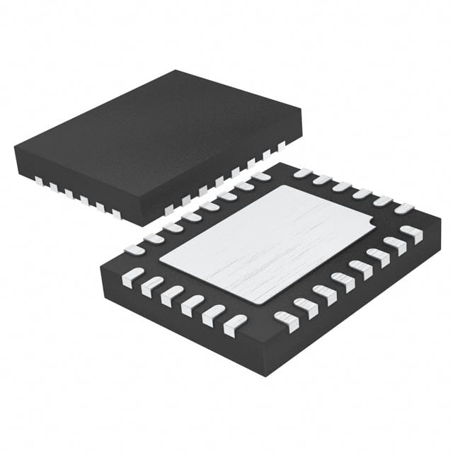
| 封装/外壳 | 28-WFQFN 裸露焊盘 |
| 工作温度 | -40°C ~ 125°C |
| 标准包装 | 73 |
| 电压-电源 | 4.5 V ~ 38 V |
| 输出数 | 1 |
| 降压 | 是 |
| 隔离式 | 无 |
| 频率-最大值 | 1MHz |


- 商务部:美国ITC正式对集成电路等产品启动337调查
- 曝三星4nm工艺存在良率问题 高通将骁龙8 Gen1或转产台积电
- 太阳诱电将投资9.5亿元在常州建新厂生产MLCC 预计2023年完工
- 英特尔发布欧洲新工厂建设计划 深化IDM 2.0 战略
- 台积电先进制程称霸业界 有大客户加持明年业绩稳了
- 达到5530亿美元!SIA预计今年全球半导体销售额将创下新高
- 英特尔拟将自动驾驶子公司Mobileye上市 估值或超500亿美元
- 三星加码芯片和SET,合并消费电子和移动部门,撤换高东真等 CEO
- 三星电子宣布重大人事变动 还合并消费电子和移动部门
- 海关总署:前11个月进口集成电路产品价值2.52万亿元 增长14.8%


PDF Datasheet 数据手册内容提取
LTC3874 PolyPhase Step-Down Synchronous Slave Controller with Sub-Milliohm DCR Sensing FEATURES DESCRIPTION n Phase Extender for High Phase Count Voltage Rails The LTC®3874 is a dual PolyPhase® current mode synchro- n Accurate Phase-to-Phase Current Sharing nous step-down slave controller. It enables high current, n Sub-Milliohm DCR Current Sensing multi-phase applications when paired with a companion n Phase-Lockable Fixed Frequency 250kHz to 1MHz master controller by extending the phase count. Compat- n Immediate Response to Master IC's Fault ible master controllers include the LTC3884, LTC3866, n Up to 12 Phase Operation LTC3875, LTC3877 and LTC3774. The LTC3874 employs a n Wide V Range: 4.5V to 38V unique architecture that enhances the signal-to-noise ratio IN n V Range: Up to 3.5V (LOWDCR Pin = INTV ) of the current sense signal, allowing the use of sub-milliohm OUT CC Up to 5.5V (LOWDCR Pin = OV) DC resistance power inductors to maximize efficiency while n Proprietary Current Mode Control Loop reducing switching jitter. Its peak current mode architecture n Programmable CCM/DCM Operation allows for accurate phase to phase current sharing even n Programmable Phase Shift Control for dynamic loads. n Dual N-Channel MOSFET Gate Drivers Effectively working with a master controller, the LTC3874 n 28-Lead (4mm × 5mm) QFN Package supports all the programmable features as well as fault protection. APPLICATIONS L, LT, LTC, LTM, Linear Technology, the Linear logo, PolyPhase and Burst Mode are registered trademarks of Analog Devices, Inc. All other trademarks are the property of their respective owners. Protected by U.S. Patents, including 5481178, 5705919, 5929620, 6100678, 6144194, n High Current Distributed Power Systems 6177787, 6304066, 6580258. n Telecom, Datacom, and Storage Systems n Intelligent Energy Efficient Power Regulation TYPICAL APPLICATION High Efficiency, 4-Phase 1.8V/120A Step-Down Supply VIN Dual Phase Efficiency and Power Loss 7V TO 14V vs Output Current, Sub-Milliohm DCR 4.7µF vs Traditional DCR VIN INTVCC LTC3874 TG0 0.33µH 100 VIN = 12V 14 PHASMD BOOST0 0.1µF (0.32mΩ DCR) VOUT 95 VCOCUMT = 1.8V 12 LOWDCR SW0 1.8V LTC3884 RRUUNN01 90k EFIRRLRXUUIETMNNVQ01CC IISSEENNSSBTEEGG00+–01 0.1µ9F03.212ΩµF 0.33µH + 4×720µF 120A EFFICIENCY (%) 889050 POWEEFRFI CLIOESNSCY 0.32mΩ 46810POWER LOSS (W) GGPPIIOO01 FFAAUULLTT01 BOOSSWT11 (0.32mΩ DCR) 75 01..352mmΩΩ 2 VVSSEENNSSEE01++ PPGGOOOOITDDH010 IMMTHOO0DDEE01 GBNGD1 931Ω + 4×720µF 700 10 L2O0AD CU3R0RENT 4(A0) 15.05mΩ 600 ITH1 ITH1 ISENSE1+ 3874 TA01b SYNC SYNC 0.22µF ISENSE1– 3874 TA02 3874fb 1 For more information www.linear.com/LTC3874
LTC3874 ABSOLUTE MAXIMUM RATINGS PIN CONFIGURATION (Note 1) V .............................................................−0.3V to 40V TOP VIEW IN R BOOST0, BOOST1 ......................................−0.3V to 46V C 0 1 D T T SW0, SW1 ....................................................−5V to 40V ITH0 LOW FAUL FAUL TG0 SW0 (BOOST0-SW0), (BOOST1-SW1) .................−0.3V to 6V 28 27 26 25 24 23 I +, I –, I +, I – ...−0.3V to INTV MODE0 1 22 BOOST0 SENSE0 SENSE0 SENSE1 SENSE1 CC ISENSE0+ 2 21 BG0 EXTV , INTV , RUN0, RUN1 ....................−0.3V to 6V CC CC ISENSE0– 3 20 VIN MODE0, MODE1, ILIM, LOWDCR, RUN0 4 29 19 INTVCC PHASMD, FREQ ....................................−0.3V to INTVcc RUN1 5 GND 18 EXTVCC SYNC, FAULT0, FAULT1, ITH0, ITH1 .........−0.3V to INTVcc ISENSE1– 6 17 BG1 INTV Peak Output Current ................................100mA ISENSE1+ 7 16 BOOST1 CC Operating Junction Temperature Range MODE1 8 15 SW1 9 10 11 12 13 14 (Note 2) ..................................................−40°C to 125°C Storage Temperature Range ..................−65°C to 150°C ITH1 FREQ ILIM SYNC ASMD TG1 H P UFD PACKAGE 28-LEAD (4mm × 5mm) PLASTIC QFN θJA = 43°C/W, θJC = 3.4°C/W EXPOSED PAD (PIN 29) IS GND, MUST BE SOLDERED TO PCB ORDER INFORMATION LEAD FREE FINISH TAPE AND REEL PART MARKING* PACKAGE DESCRIPTION TEMPERATURE RANGE LTC3874EUFD#PBF LTC3874EUFD#TRPBF 3874 28-Lead (4mm × 5mm) Plastic QFN –40°C to 125°C LTC3874IUFD#PBF LTC3874IUFD#TRPBF 3874 28-Lead (4mm × 5mm) Plastic QFN –40°C to 125°C Consult LTC Marketing for parts specified with wider operating temperature ranges. *The temperature grade is identified by a label on the shipping container. For more information on lead free part marking, go to: http://www.linear.com/leadfree/ For more information on tape and reel specifications, go to: http://www.linear.com/tapeandreel/. Some packages are available in 500 unit reels through designated sales channels with #TRMPBF suffix. 3874fb 2 For more information www.linear.com/LTC3874
LTC3874 ELECTRICAL CHARACTERISTICS The l denotes the specifications which apply over the specified operating junction temperature range, otherwise specifications are at T = 25°C (Note 2). V = 12V, V = 3.3V unless otherwise specified. A IN RUN0,1 SYMBOL PARAMETER CONDITIONS MIN TYP MAX UNITS Input Voltage V Input Voltage Range 4.5 38 V IN V Output Voltage Range LOWDCR = INTV (Note 3) 3.5 V OUT CC LOWDCR = 0V 5.5 V I Input DC Supply Current (Note 4) Q Normal Operation V = 3.3V 4.6 mA RUN0,1 Shutdown V = 0V 1.8 mA RUN0,1 V Undervoltage Lockout Threshold V Falling 3.5 V UVLO INTVCC V Rising 3.8 V INTVCC Control Loop I I Pins Bias Current V < (V – 3.3V) l ±0.15 ±0.4 µA ISENSE0,1 SENSE ISENSE0,1 INTVCC V > (V – 3.3V) l ±1 ±3 µA ISENSE0,1 INTVCC V Maximum Current Sense Threshold (Table 3) ISENSE(MAX) ILIM = INTV , LOWDCR = INTV , l 26.8 28.8 30.8 mV CC CC V = 1.2V, V = 2.18V ISENSE0,1 ITH ILIM = 0V, LOWDCR = INTV , l 14.5 16 17.5 mV CC V = 1.2V, V = 2.18V ISENSE0,1 ITH ILIM = INTV , LOWDCR = 0V, l 65 72 79 mV CC V = 1.2V, V = 2.18V ISENSE0,1 ITH ILIM = 0V, LOWDCR = 0V, l 33 40 47 mV V = 1.2V, V = 2.18V ISENSE0,1 ITH Gate Drivers TG R TG Pull-Up R TG High 2.6 Ω UP DS(ON) TG R TG Pull-Down R TG Low 1.5 Ω DOWN DS(ON) BG R BG Pull-Up R BG High 2.4 Ω UP DS(ON) BG R BG Pull-Down R BG Low 1.1 Ω DOWN DS(ON) TG0,1 TG Transition Time: (Note 5) t Rise Time C = 3300pF 30 ns r LOAD t Fall Time C = 3300pF 30 ns f LOAD BG0,1 BG Transition Time: (Note 5) t Rise Time C = 3300pF 30 ns r LOAD t Fall Time C = 3300pF 30 ns f LOAD TG/BG t Top Gate Off to Bottom Gate on Delay Time C = 3300pF Each Driver (Note 5) 30 ns 1D LOAD BG/TG t Bottom Gate Off to Top Gate On Delay Time C = 3300pF Each Driver (Note 5) 30 ns 2D LOAD t Minimum On-Time (Note 6) 60 ns ON(MIN) INTV Regulator CC V Internal V Voltage No Load 6V < V < 38V 5.25 5.5 5.75 V INTVCC CC IN V INT INTV Load Regulation I = 0mA to 20mA 0.5 2 % LDO CC CC V EXTV Switchover Voltage EXTV Ramping Positive (Note 7) l 4.5 4.7 V EXTVCC CC CC V EXT EXTV Voltage Drop I = 20mA, V = 5V 50 100 mV LDO CC CC EXTVCC V EXTV Hysteresis 300 mV LDOHYS CC 3874fb 3 For more information www.linear.com/LTC3874
LTC3874 ELECTRICAL CHARACTERISTICS The l denotes the specifications which apply over the specified operating junction temperature range, otherwise specifications are at T = 25°C (Note 2). V = 12V, V = 3.3V unless otherwise specified. A IN RUN0,1 SYMBOL PARAMETER CONDITIONS MIN TYP MAX UNITS Oscillator and Phase-Locked Loop f PLL SYNC Range l 250 1000 kHz RANGE f Nominal Frequency V = 0.9V 500 kHz NOM FREQ I Frequency Setting Current 9 10 11 µA FREQ θ SYNC-θ0 SYNC to Ch0 Phase Relationship Based on PHASMD = 0 180 Deg the Falling Edge of SYNC and Rising Edge PHASMD = 1/3 • INTV 60 Deg CC of TG0 PHASMD = 2/3 • INTV 120 Deg CC PHASMD = INTV 90 Deg CC θ SYNC-θ1 SYNC to Ch1 Phase Relationship Based on PHASMD = 0 0 Deg the Falling Edge of SYNC and Rising Edge PHASMD = 1/3 • INTV 300 Deg CC of TG1 PHASMD = 2/3 • INTV 240 Deg CC PHASMD = INTV 270 Deg CC Digital Inputs RUN0, RUN1, MODE0, MODE1, FAULT0, FAULT1, LOWDCR V Input High Threshold Voltage l 2.0 V IH V Input Low Threshold Voltage l 1.4 V IL Note 1: Stresses beyond those listed under Absolute Maximum Ratings Note 3: Output voltage is set and controlled by master controller in may cause permanent damage to the device. Exposure to any Absolute multiphase operations. Maximum Rating condition for extended periods may affect device Note 4: Dynamic supply current is higher due to the gate charge being reliability and lifetime. delivered at the switching frequency. See Application Information. Note 2: The LTC3874 is tested under pulsed load conditions such that Note 5: Rise and fall times are measured using 10% and 90% levels. Delay T ≈ T . The LTC3874E is guaranteed to meet performance specifications times are measured using 50% levels. J A from 0°C to 85°C. Specifications over the –40°C to 125°C operating Note 6: The minimum on-time condition corresponds to an inductor junction temperature range are assured by design, characterization and peak-to-peak ripple current ≥ 40% of I (see Minimum On-Time MAX correlation with statistical process controls. The LTC3874I is guaranteed Considerations in the Applications Information section). over the –40°C to 125°C operating junction temperature range. High Note 7: EXTV is enabled only if V is higher than 7V. CC IN junction temperatures degrade operating lifetimes; operating lifetime is derated for junction temperatures greater than 125°C. Note that the maximum ambient temperature consistent with these specifications is determined by specific operating conditions in conjunction with board layout, the rated package thermal impedance and other environmental factors. T is calculated from the ambient temperature T and power J A dissipation P according to the following formula: D T = T + (P • 43˚C/W) J A D 3874fb 4 For more information www.linear.com/LTC3874
LTC3874 TYPICAL PERFORMANCE CHARACTERISTICS (T = 25°C unless otherwise specified) A Efficiency vs Output Current Efficiency vs Output Current Dual Phase Efficiency and Power and Mode and Mode Loss vs Output Current 100 100 100 14 VIN = 12V 90 90 VOUT = 1.8V 95 CCM 12 80 80 DCM EFFICIENCY (%) 75640000 DCM CCM VVIONU =T =1 21V.2V EFFICIENCY (%) 75640000 CCM VVIONU =T =1 21V.8V EFFICIENCY (%) 889050 POWEEFRFI CLIOESNSCY 6810POWER LOSS (W 30 30 4 ) 0.32mΩ 20 20 75 1.5mΩ 2 10 10 0.32mΩ 1.5mΩ 0 0 70 0 0.1 1 10 100 0.1 1 10 100 0 10 20 30 40 50 60 LOAD CURRENT (A) LOAD CURRENT (A) LOAD CURRENT (A) 3874 G01 3874 G02 3874 G03 Load Step (Forced Continuous Load Step (Discontinuous Mode) 3-Phase with Master Conduction Mode) 3-Phase with Controller LTC3866 Master Controller LTC3866 IL(MASTER) IL(MASTER) 20A/DIV 20A/DIV IL(SLAVE1) IL(SLAVE1) 20A/DIV 20A/DIV IL(SLAVE0) IL(SLAVE0) 20A/DIV 20A/DIV VOUT VOUT 200mV/DIV 200mV/DIV AC-COUPLED 50µs/DIV 3874 G04 AC-Coupled 50µs/DIV 3874 G05 VIN = 12V VIN = 12V VOUT = 1.2V VOUT = 1.2V ILOAD 5A TO 50A ILOAD 5A TO 50A Start-Up Into a Pre-Biased Output Inductor Current at Light Load with Master Controller LTC3875 FORCED CONTINUOUS RUN MODE 5V/DIV 5A/DIV OV DISCONTINUOUS VOUT CONDUCTION 1V/DIV MODE OV 5A/DIV 1µs/DIV 3874 G06 20ms/DIV 3874 G06a VIN = 12V VIN = 12V VOUT = 1.2V VOUT = 1.0V ILOAD = 2A 3874fb 5 For more information www.linear.com/LTC3874
LTC3874 TYPICAL PERFORMANCE CHARACTERISTICS (T = 25°C unless otherwise specified) A Quiescent Current Current Sense Threshold vs Temperature without EXTV INTV Line Regulation vs I Voltage CC CC TH 6 6 100 LOWDCR = L, RANGE = H 5 5 80 A) CURRENT (m 43 OLTAGE (V) 43 (mV)SE 4600 LROAWNGDEC R= L= L, UIESCENT 2 INTV VCC 2 VISEN 200 LROAWNGDEC R= L= H, Q 1 1 –20 LOWDCR = H, RANGE = H 0 0 –40 –50 –5 45 95 125 0 5 10 15 20 25 30 35 40 0 0.5 1 1.5 2 2.5 3 TEMPERATURE (°C) VIN (V) VITH (V) 3874 G07 3874 G08 3874 G09 Maximum Current Sense Threshold vs Common Mode Voltage (LOWDCR = INTV , Undervoltage Lockout Threshold Quiescent Current CC V = 2.18V) (INTV ) vs Temperature vs Input Voltage without EXTV ITH CC CC 30 4.1 5.5 V) ILIM = INTVCC 3.9 RISING 5.3 ENT SENSE THRESHOLD (m 12210055 ILIM = GND UVLO THRESHOLD (V) 23333.....97153 FALLING SUPPLY CURRENT (mA) 544444......131579 RR 3.9 U 5 C 2.7 3.7 0 2.5 3.5 0 0.5 1.0 1.5 2.0 2.5 3.0 3.5 –50 –5 45 95 125 5 10 15 20 25 30 35 40 VISENSE COMMON MODE VOLTAGE (V) TEMPERATURE (°C) VIN (V) 3874 G10 3874 G12 3874 G14 3874fb 6 For more information www.linear.com/LTC3874
LTC3874 PIN FUNCTIONS MODE0/MODE1 (PIN 1/Pin 8): DCM/CCM Mode Control source. Voltage swing at the pins are from a Schottky pins. Each channel runs in forced continuous mode if the diode (external) voltage drop below ground to V . IN Mode pin is logic high. There is an internal 500k pull-down BOOST0/BOOST1 (Pin 22/Pin 16): Boosted Floating Driver resistor on Mode pin. To select discontinuous conduction Supplies. The (+) terminal of the bootstrap capacitors con- mode, float or pull down the MODE pin. nect to these pins. These pins swing from a diode voltage I +/I + (Pin 2/Pin 7): Current Sense Compara- drop below INTV up to V + INTV . SENSE0 SENSE1 CC IN CC tor Inputs. The (+) inputs to the current comparators are BG0/BG1 (Pin 21/Pin 17): Bottom Gate Driver Outputs. normally connected to DCR sensing networks. These pins drive the gates of the bottom N-channel MOS- I −/I − (Pin 3/Pin 6): Current Sense Compara- FETs between GND and INTV . SENSE0 SENSE1 CC tor Inputs. The (−) inputs to the current comparators are EXTV (Pin 18): External Power Input to an Internal Switch CC connected to the outputs. Connected to INTV . The switch closes and supplies the CC RUN0/RUN1 (Pin 4/Pin 5): Enable Run Inputs. Logic high IC power, bypassing the internal low dropout regulator, on RUN pin enables the corresponding channel. whenever EXTV is higher than 4.7V and V is greater CC IN than 7V. Do not exceed 6V on this pin. I /I (Pin 28/Pin 9): Current Control Threshold. Each TH0 TH1 associated channel’s current comparator tripping threshold INTV (Pin 19): Internal 5.5V Regulator Output. The con- CC increases with its I voltage. These pins must be con- trol circuits are powered from this voltage. Decouple this TH nected to the master controller’s I pins. pin to GND with a minimum of 4.7μF low ESR tantalum TH or ceramic capacitor. FREQ (Pin 10): Frequency Set Pin. There is a precision 10µA current flowing out of this pin. A resistor to ground V (Pin 20): Main Input Supply. Decouple this pin to GND IN sets a voltage which in turn programs the frequency. This with a capacitor (0.1μF to 1μF). pin sets the default switching frequency when there is no FAULT0, FAULT1 (Pin 26/Pin 25): Master Controller Fault external clock on the SYNC pin. See the application section Inputs. Connect these pins to the master chip fault indica- for detailed information. tor pins to respond to the fault signals from the master ILIM (Pin 11): Current Comparators Sense Voltage Limit. controller. When a FAULT pin is floating or low, both TG Program a DC voltage at this pin to set the maximum cur- and BG pins are pulled down in the corresponding chan- rent sense threshold for the current comparators. nel. There is an internal 500k pull-down resistor on each FAULT pin. SYNC (Pin 12): External Clock Synchronization Input. If an external clock is present at this pin, the switching frequency LOWDCR (Pin 27): Sub-milliohm DCR Current Sensing will be synchronized to the falling edge of external clock. Enable Pin. There is an internal 500k pull-up resistor be- Tie this pin to GND if not used. tween LOWDCR pin and INTV . Floating or pulling this CC pin logic high will enable the sub-milliohm DCR current PHASMD (Pin 13): Phase Set Pin. This pin determines the sensing. Puling this pin logic low will disable the sub- relative phases between the external clock on pin SYNC milliohm DCR current sensing. and the internal controllers. See Table 1 in the Operation section for details. GND (Exposed Pad Pin 29): Ground. Connect this pad, through vias, to a solid ground plane under the circuit. TG0/TG1 (Pin 24/Pin 14): Top Gate Driver Outputs. These The sources of the bottom N-channel MOSFETs, the (–) are the outputs of floating drivers with a voltage swing terminal of C , and the (–) terminal of C should equal to INTV superimposed on the switch node voltages. INTVCC IN CC connect to this ground plane as closely as possible to SW0/SW1 (Pin 23/Pin 15): Switch Node Connections. the IC. All small-signal components and compensation Connect these pins to the output filter inductor, bottom components should also connect to this ground plane. N-channel MOSFET drain and top N-channel MOSFET 3874fb 7 For more information www.linear.com/LTC3874
LTC3874 FUNCTIONAL BLOCK DIAGRAM One of Two Channels (CH0) Shown 10µA SYNC PHASMD EXTVCC 4.7V FREQ SYNC/PHASE VIN DETECT + – VIN + PLL-SYNC CIN OSC 5.5V REG S R Q INTVCC ICMP 5K IREV + – BOOST0 – + TG0 CB ON M1 REV SWITCH SW0 LOGIC UVLO AND ILIM ILIM RANGE SELECT 1 FAULTB ANTI- DB + VOUT0 LHOI: :1 1:1:1.8 5k FCNT THSHROOOUTG-H BG0 COUT0 DC RUN M2 AMP GND CVCC COMPSELNOSPAETION ISENSE0+ INTVCC UVLO ISENSE0– 1 INTVCC 60k + – + – + – + – 1.7V REF ITH0 LOWDCR MODE0 RUN0 FAULT0 3874 BD 3874fb 8 For more information www.linear.com/LTC3874
LTC3874 OPERATION Main Control Loop INTV /EXTV Power CC CC The LTC3874 is a constant frequency, LTC proprietary cur- Power for the top and bottom MOSFET drivers and most rent mode step-down slave controller for parallel operation other internal circuitry is derived from the INTV pin. CC with master controllers. During normal operation, each When the EXTV pin is left open or tied to a voltage less CC top MOSFET is turned on when the clock for that channel than 4.7V, an internal 5.5V linear regulator supplies INTV CC sets the RS latch, and turned off when the main current power from V . If EXTV is taken above 4.7V and V IN CC IN comparator, I , resets the RS latch. The peak inductor is higher than 7V, the 5.5V regulator is turned off and an CMP current at which I resets the RS latch is controlled by internal switch is turned on connecting EXTV . EXTV CMP CC CC the voltage on the I pin, which is the output of the master can be applied before V . Using the EXTV allows the TH IN CC controller. When the load current increases, the master INTV power to be drawn from an external source. CC controller increases the I voltage, which in turn causes TH Each top MOSFET driver is biased from the floating boot- the peak current in the corresponding slave channels to strap capacitor C , which normally recharges during each B increase, until the average inductor current matches the off cycle through an external diode when the top MOSFET new load current. After the top MOSFET has turned off, turns off. If the input voltage V decreases to a voltage IN the bottom MOSFET is turned on until the beginning of close to V , the loop may enter dropout and attempt to OUT the next cycle in Continuous Conduction Mode (CCM) or turn on the top MOSFET continuously. A dropout detector until the inductor current starts to reverse, as indicated detects this and forces the top MOSFET off for about one- by the reverse current comparator I , in Discontinuous REV twelfth of the clock period plus 100ns every three cycles Conduction Mode (DCM). The LTC3874 slave controllers to allow C to recharge. B DO NOT regulate the output voltage but regulate the cur- rent in each channel for current sharing with the master Start-Up and Shutdown (RUN0, RUN1) controllers. Output voltage regulation is achieved through The two channels of the LTC3874 can be independently the voltage feedback control loop in the master controllers. shut down using the RUN0 and RUN1 pins. Pulling either Sub-Milliohm DCR Current Sensing of these pins below 1.4V shuts down the main control circuits for that channel. During shutdown, both TG The LTC3874 employs a unique architecture to enhance and BG are pulled down to turn off the external power the signal-to-noise ratio that enables it to operate with MOSFETs. Pulling either of these pins above 2V enables a small sense signal of a sub-milliohm value inductor the controller. The RUN0/1 pins are actively pulled down DCR to improve power efficiency and reduce jitter due to until the INTV voltage passes the undervoltage lockout CC switching noise. threshold of 3.8V. For multiphase operation, the RUN0/1 Floating or pulling the LOWDCR pin high will enable sub- pins must be connected together and driven by the RUN milliohm DCR current sensing. The LTC3874 can sense pins on the master controller. Because a large RC filter in a DCR value as low as 0.2mΩ with careful PCB layout. the LTC3874 needs to settle during initialization, the RUN The proprietary signal processing circuit provides a 14dB pins can only be pulled up 4ms after V is ready. Do not IN signal-to-noise ratio improvement. As with conventional exceed the Absolute Maximum Rating of 6V on these pins. current mode architectures, the current limit threshold is still a function of the inductor peak current and the DCR value, and can be accurately set with the ILIM and I pins. TH 3874fb 9 For more information www.linear.com/LTC3874
LTC3874 OPERATION The start-up of each channel’s output voltage V is OUT Table 1 controlled by the master controller. After the RUN pins are PHASMD CHANNEL 0 PHASE CHANNEL 1 PHASE released, the master controller drives the output based on GND 180° 0° the programmed delay time and rise time. The slave con- 1/3 INTV 60° 300° CC troller LTC3874 follows the I voltage set by the master TH 2/3 INTV or Float 120° 240° CC to supply the same current to the output during startup. INTV 90° 270° CC Light Load Current Operation (Discontinuous The SYNC pin is used to synchronize switching frequency Conduction Mode, Continuous Conduction Mode) between the master and slave controllers. Input capacitance The LTC3874 can operate either in discontinuous conduc- ESR requirements and efficiency losses are substantially tion mode or forced continuous conduction mode. To reduced because the peak current drawn from the input select forced continuous mode, tie the MODE pin to a DC capacitor is effectively divided by the number of phases voltage above 2V (e.g., INTV ). To select discontinuous used and power loss is proportional to the RMS current CC conduction mode, tie the MODE pin to a DC voltage below squared. A two stage, single output voltage implementa- 1.4V (e.g., GND).In forced continuous mode, the induc- tion can reduce input path power loss by 75% and radi- tor current is allowed to reverse at light loads or under cally reduce the required RMS current rating of the input large transient conditions. The peak inductor current is capacitor(s). determined by the voltage on the I pin. In this mode, the TH efficiency at light loads is lower than in discontinuous mode. Single Output Multiphase Operation However, continuous mode has the advantages of lower The LTC3874 is configured for single output multiphase output ripple and less interference with audio circuitry. converters with a master controller by making these When the MODE pin is connected to GND, the LTC3874 connections operates in discontinuous mode at light loads. At very light • Tie all the I pins of paralleled channels together for loads, the current comparator I may remain tripped for TH CMP current sharing between masters and slaves; several cycles and force the external top MOSFET to stay off for the same number of cycles (i.e., skipping pulses). • Tie all SYNC or PLLIN pins of paralleled channels to- This mode provides higher light load efficiency than forced gether or tie the master chip’s CLKOUT pin to the slave continuous mode and the inductor current is not allowed chip’s SYNC pin for switching frequency synchronization to reverse. There is a 500k pull-down resistor internally among channels. connected to the MODE pin. If the MODE0/1 pins are left • Tie all the RUN pins of paralleled channels together for floating, both channels are in discontinuous conduction startup and shutdown at the same time. mode by default. • Tie the fault indictor pin of the master controller if avail- Multichip Operations (PHASMD and SYNC Pins) able to the FAULT pin of the slave controller for fault protection. The PHASMD pin determines the relative phases between the internal channels as well as the external clock signal on • The LTC3874 MODE pin can be tied to the master chip SYNC pin as shown in Table 1. The phases tabulated are PGOOD pin for start-up control. During soft-start, the relative to zero degree phase being defined as the falling LTC3874 operates in DCM mode. When the soft-start edge of the clock on SYNC pin. interval is done, the LTC3874 operates in CCM mode. Examples of single output multiphase converters are shown in Figure 1. 3874fb 10 For more information www.linear.com/LTC3874
LTC3874 OPERATION 3 PHASE OPERATION 3 PHASE + 1 PHASE OPERATION CH0 CH1 CH1 CH2 CH0 CH1 0° 240° 120° 0° 180° 60° 300° LTC3866 LTC3874 LTC3884 LTC3874 CLKOUT SYNC SYNC SYNC PHASMD = 1/3 INTVCC PHASMD = 1/3 INTVCC 4 PHASE OPERATION 4 PHASE OPERATION CH1 CH2 CH0 CH1 CH1 CH2 CH0 CH1 0° 180° 90° 270° 0° 180° 90° 270° LTC3875 LTC3874 LTC3884 LTC3874 CLKOUT SYNC SYNC SYNC PHASMD = FLOAT PHASMD = GND PHASMD = INTVCC 6 PHASE OPERATION 6 PHASE OPERATION CH1 CH2 CH0 CH1 CH0 CH1 CH1 CH2 CH0 CH1 CH0 CH1 0° 240° 120° 300° 60° 180° 0° 180° 60° 300° 120° 240° LTC3875 LTC3874 LTC3874 LTC3884 LTC3874 LTC3874 CLKOUT SYNC SYNC SYNC SYNC SYNC PHASMD = INTVCC PHASMD = GND PHASMD = 2/3 INTVCC PHASMD = 1/3 INTVCC PHASMD = 2/3 INTVCC 3874 F01 Figure 1. Multiphase Operation Frequency Selection and Phase-Locked Loop user can program the controller’s switching frequency with (FREQ and SYNC Pins) a single resistor to GND. A curve is provided later in the application section showing the relationship between the The selection of switching frequency is a trade-off between voltage on the FREQ pin and switching frequency (Figure efficiency and component size. Low frequency operation 5). A phase-locked loop (PLL) is integrated in the LTC3874 increases efficiency by reducing MOSFET switching losses, to synchronize the internal oscillator to an external clock but requires larger inductance and/or capacitance to main- source on the SYNC pin. The PLL loop filter network is tain low output ripple voltage. The switching frequency of integrated inside the LTC3874. The phase-locked loop is the LTC3874 controllers can be selected using the FREQ capable of locking to any frequency within the range of pin. If the SYNC pin is not being driven by an external clock 250kHz to 1MHz. The frequency setting resistor should source, the FREQ pin can be used to program the control- always be present to set the controller’s initial switching ler’s operating frequency from 250kHz to 1MHz. There is a frequency before locking to the external clock. precision 10µA current flowing out of the FREQ pin, so the 3874fb 11 For more information www.linear.com/LTC3874
LTC3874 APPLICATIONS INFORMATION The Typical Application on the first page of this data Table 3. Current Sense Threshold vs I Voltage TH sheet is a basic LTC3874 application circuit configured CURRENT SENSE THRESHOLD (mV) as a slave controller. In paralleled operation, the current LOWDCR = H LOWDCR = L sensing scheme and circuit parameters in the LTC3874 I (V) RANGE = H RANGE = L RANGE = H RANGE = L TH have to be the same as the master controller to achieve 2.40 32.5 18.1 81.3 45.1 balanced current sharing between masters and slaves. 2.33 31.4 17.4 78.4 43.6 Input and output capacitors are selected based on RMS 2.26 30.2 16.8 75.6 42.0 current rating, ripple and transient specs. 2.20 29.1 16.2 72.7 40.4 2.18 28.8 16.0 72.0 40.0 Current Limit Programming 2.13 28.0 15.5 69.9 38.8 To match the master controller current limit, each chan- 2.06 26.8 14.9 67.1 37.3 nel of the LTC3874 can be programmed separately with 1.99 25.7 14.3 64.2 35.7 the ILIM and LOWDCR pins. The 4-level logic input pin 1.92 24.6 13.6 61.4 34.1 ILIM setup summary is shown in Table 2. When ILIM is 1.85 23.4 13.0 58.5 32.5 grounded, both channels are set to be low current range. 1.79 22.3 12.4 55.7 30.9 When ILIM is tied to INTV , both channels are set to be CC 1.72 21.1 11.7 52.8 29.4 high current range. 1.68 20.4 11.3 51.0 28.4 Which setting should be used? For balanced load cur- 1.58 18.9 10.5 47.2 26.2 rent sharing, use the same current range setting as in 1.51 17.7 9.9 44.3 24.6 the master controller. Note, the LTC3874 does not have 1.45 16.6 9.2 41.5 23.0 active clamping circuit on I pin for peak current limit 1.38 15.5 8.6 38.6 21.4 TH and over current protection. Over current protection relies on the master controller to drive the ITH pin not to exceed ISENSE+ and ISENSE− Pins the clamped voltage. The relationship between the current I + and I – are the inputs to the current com- sense threshold and I voltage can be found in Table 3. SENSE SENSE TH parators. When the LOWDCR pin is high, their common Table 2. ILIM vs Range mode input voltage range is 0V to 3.5V. I – should SENSE CHANNEL 0 CHANNEL 1 be connected directly to VOUT of the master controller. ILIM CURRENT LIMIT CURRENT LIMIT I + is connected to an R • C filter with time constant SENSE GND Range Low Range Low one-fifth of L/DCR of the output inductor. Care must be 1/3 INTVCC Range High Range Low taken not to float these pins during normal operation. 2/3 INTVCC or Float Range Low Range High Filter components, especially capacitors, must be placed INTVcc Range High Range High close to the LTC3874, and the sense lines should run close 3874fb 12 For more information www.linear.com/LTC3874
LTC3874 APPLICATIONS INFORMATION together to a Kelvin connection underneath the current than 1mΩ for high current inductors. In high current and sense element. The LTC3874 is designed to be used with low output voltage applications, conduction loss of a high a sub-milliohm DCR value; without proper care, parasitic DCR or a sense resistor will cause a significant reduction resistance, capacitance and inductance will degrade the in power efficiency. For a specific output requirement, current sense signal integrity, making the programmed choose the inductor with the DCR that satisfies the maxi- current limit unpredictable. In Figure 2, resistor R must be mum desirable sense voltage, and use the relationship of placed close to the output inductor and capacitor C close to the sense pin filters to output inductor characteristics as the IC pins to prevent noise coupling to the sense signal. depicted below. The LTC3874 can also be used like any conventional cur- V ISENSE(MAX) DCR= rent mode controller by disabling the LOWDCR pin, con- ΔI I + L necting it to ground. An RC filter can be used to sense the MAX 2 output inductor signal and connects to the I + pin. Its SENSE time constant, R • C, should equal to L/DCR of the output RC = L/(5 • DCR) when the LOWDCR pin is high inductor. By pulling down the LOWDCR pin, the current RC = L/DCR when the LOWDCR pin is low limit increases by 2.5 times. See Table 3 for details. In these applications, the common mode operating voltage where: range of I +, I – is from 0V to 5.5V. SENSE SENSE V : Maximum sense voltage for a given I ISENSE(MAX) TH voltage Table 4. Output Voltage Range vs LOWDCR Pin LOWDCR OUTPUT VOLTAGE I : Maximum load current MAX Low 0V to 5.5V ΔI : Inductor ripple current L High 0V to 3.5V L, DCR: Output inductor characteristics R, C: Filter time constant VIN VIN INTVCC To ensure that the load current will be delivered over the full LTC3874 operating temperature range, the temperature coefficient BOOST INDUCTANCE of the DCR resistance, approximately 0.4%/°C, should be TG L DCR taken into consideration. SW VOUT BG Typically, C is selected in the range of 0.047µF to 0.47µF. GND This forces R to around 2kΩ, reducing error that might R ISENSE+ have been caused by the ISENSE pins’ ±1uA current. C ISENSE– There will be some power loss in R that relates to the duty cycle. It will be highest in continuous mode at maximum 3874 F02 input voltage: Figure 2 Inductor DCR Current Sensing ( ) V −V (cid:127)V IN(MAX) OUT OUT P (R)= LOSS Inductor DCR Current Sensing R The LTC3874 is specifically designed for high load current Ensure that R has a power rating higher than this value. applications requiring the highest possible efficiency; it is However, DCR sensing eliminates the conduction loss capable of sensing the signal of an inductor DCR in the of a sense resistor; it will provide a better efficiency at sub-milliohm range (Figure 2). The DCR is the DC winding heavy loads. To maintain a good signal-to-noise ratio for resistance of the inductor’s copper, which is often less the current sense signal, using a minimum ΔV of ISENSE 3874fb 13 For more information www.linear.com/LTC3874
LTC3874 APPLICATIONS INFORMATION 2mV for duty cycles less than 40% is desirable when the concentrate on copper loss and preventing saturation. LOWDCR pin is high; use a minimum ΔV of 10mV Ferrite core material saturates “hard,” which means that ISENSE for duty cycles less than 40% when the LOWDCR pin is inductance collapses abruptly when the peak design current low. The actual ripple voltage will be determined by the is exceeded. This results in an abrupt increase in inductor following equation: ripple current and consequent output voltage ripple. Do not allow the core to saturate! V ⎛ V −V ⎞ ΔV = OUT IN OUT ISENSE ⎜ ⎟ V ⎝ RC(cid:127)f ⎠ Power MOSFET and Schottky Diode IN OSC (Optional) Selection Inductor Value Calculation At least two external power MOSFETs need to be selected: One N-channel MOSFET for the top (main) switch and one Given the desired input and output voltages, the inductor or more N-channel MOSFET(s) for the bottom (synchro- value and operating frequency, f , directly determine OSC nous) switch. The number, type and on-resistance of all the inductor’s peak-to-peak ripple current: MOSFETs selected take into account the voltage step-down V ⎛ V –V ⎞ ratio as well as the actual position (main or synchronous) I = OUT IN OUT RIPPLE V ⎝⎜ f (cid:127)L ⎠⎟ in which the MOSFET will be used. A much smaller and IN OSC much lower input capacitance MOSFET should be used Lower ripple current reduces core losses in the inductor, for the top MOSFET in applications that have an output ESR losses in the output capacitors, and output voltage voltage that is less than one-third of the input voltage. In ripple. Thus, highest efficiency operation is obtained at applications where VIN >> VOUT , the top MOSFETs’ on- low frequency with a small ripple current. Achieving this, resistance is normally less important for overall efficiency however, requires a large inductor. than its input capacitance at operating frequencies above 300kHz. MOSFET manufacturers have designed special A reasonable starting point is to choose a ripple current purpose devices that provide reasonably low on-resistance that is about 40% of I . Note that the largest ripple OUT(MAX) with significantly reduced input capacitance for the main current occurs at the highest input voltage. To guarantee switch application in switching regulators. that ripple current does not exceed a specified maximum, the inductor should be chosen according to: The peak-to-peak MOSFET gate drive levels are set by the internal regulator voltage, V , requiring the use of V –V V INTVCC L≥ IN OUT (cid:127) OUT logic-level threshold MOSFETs in most applications. Pay fOSC(cid:127)IRIPPLE VIN close attention to the BV specification for the MOSFETs DSS as well; many of the logic-level MOSFETs are limited to Inductor Core Selection 30V or less. Selection criteria for the power MOSFETs Once the inductance value is determined, the type of in- include the on-resistance, RDS(ON), input capacitance, ductor must be selected. Core loss is independent of core input voltage and maximum output current. MOSFET input capacitance is a combination of several components but size for a fixed inductor value, but it is very dependent on inductance selected. As inductance increases, core losses can be taken from the typical gate charge curve included on most data sheets (Figure 3). The curve is generated by go down. Unfortunately, increased inductance requires forcing a constant input current into the gate of a common more turns of wire and therefore copper losses will increase. source, current source loaded stage and then plotting the Ferrite designs have very low core loss and are preferred gate voltage versus time. at high switching frequencies, so design goals can 3874fb 14 For more information www.linear.com/LTC3874
LTC3874 APPLICATIONS INFORMATION The power dissipation for the main and synchronous VIN MOSFETs at maximum output current are given by: MILLER EFFECT VGS V P = VOUT(I )2(1+δ)R + a b MAIN MAX DS(ON) + V IN + VDS QIN VGS – ⎛I ⎞ CMILLER = (QB – QA)/VDS – (V )2 MAX (R )(C )(cid:127) 3874 F03 IN ⎝⎜ 2 ⎠⎟ DR MILLER Figure 3. Gate Charge Characteristic ⎡ 1 1 ⎤ ⎢ + ⎥(cid:127)f The initial slope is the effect of the gate-to-source and ⎣⎢VINTVCC –VTH(MIN) VTH(MIN)⎦⎥ the gate-to-drain capacitance. The flat portion of the curve is the result of the Miller multiplication effect of the PSYNC = VIN–VOUT(IMAX)2(1+δ)RDS(ON) V drain-to-gate capacitance as the drain drops the voltage IN across the current source load. The upper sloping line is where δ is the temperature dependency of R , R DS(ON) DR due to the drain-to-gate accumulation capacitance and is the effective top driver resistance (approximately 2Ω at the gate-to-source capacitance. The Miller charge (the V = V ), V is the drain potential and the change GS MILLER IN increase in coulombs on the horizontal axis from a to b in drain potential in the particular application. V TH(MIN) while the curve is flat) is specified for a given V drain DS is the data sheet specified typical gate threshold voltage voltage, but can be adjusted for different V voltages by DS specified in the power MOSFET data sheet at the specified multiplying the ratio of the application V to the curve DS drain current. C is the calculated capacitance using MILLER specified V values. A way to estimate the C term DS MILLER the gate charge curve from the MOSFET data sheet and is to take the change in gate charge from points a and b the technique described above. on a manufacturer’s data sheet and divide by the stated Both MOSFETs have I2R losses while the topside N-channel V voltage specified. C is the most important se- DS MILLER equation includes an additional term for transition losses, lection criteria for determining the transition loss term in which peak at the highest input voltage. For V < 20V, the top MOSFET but is not directly specified on MOSFET IN the high current efficiency generally improves with larger data sheets. C and C are specified sometimes but RSS OS MOSFETs, while for V > 20V, the transition losses rapidly definitions of these parameters are not included. When the IN increase to the point that the use of a higher R device controller is operating in continuous mode the duty cycles DS(ON) with lower C actually provides higher efficiency. The for the top and bottom MOSFETs are given by: MILLER synchronous MOSFET losses are greatest at high input V voltage when the top switch duty factor is low or during MainSwitchDutyCycle= OUT V a short-circuit when the synchronous switch is on close IN to 100% of the period. ⎛V –V ⎞ SynchronousSwitchDutyCycle=⎜ IN OUT⎟ The term (1 + δ ) is generally given for a MOSFET in the ⎝ V ⎠ IN form of a normalized R vs temperature curve, but DS(ON) δ = 0.005/°C can be used as an approximation for low voltage MOSFETs. 3874fb 15 For more information www.linear.com/LTC3874
LTC3874 APPLICATIONS INFORMATION An optional Schottky diode across the synchronous the LTC3874 INTV current is limited to less than 34mA CC MOSFET conducts during the dead time between the con- from a 38V supply in the UFD package and not using the duction of the two large power MOSFETs. This prevents the EXTV supply: CC body diode of the bottom MOSFET from turning on, storing T = 70°C + (34mA)(38V)(43°C/W) = 125°C J charge during the dead time and requiring a reverse-recov- ery period which could cost as much as several percent in To prevent the maximum junction temperature from being efficiency. A 2A to 8A Schottky is generally a good com- exceeded, the input supply current must be checked while promise for both regions of operation due to the relatively operating in continuous conduction mode (MODE = INTVCC) small average current. Larger diodes result in additional at maximum VIN. When the voltage applied to EXTVCC rises transition loss due to their larger junction capacitance. above 4.7V and VIN above 7V, the INTVCC linear regula- tor is turned off and the EXTV is connected to INTV . CC CC INTV Regulators and EXTV Using the EXTV allows the MOSFET driver and control CC CC CC power to be derived from other high efficiency sources The LTC3874 features a PMOS LDO that supplies power such as +5V rails in the system. Do not apply more than to INTV from the V supply. INTV powers the gate CC IN CC 6V to the EXTV pin. drivers and most of the LTC3874’s internal circuitry. The CC linear regulator regulates the voltage at the INTV pin Significant efficiency and thermal gains can be realized CC to 5.5V when V is greater than 6V. EXTV connects by powering INTV from EXTV . Tying the EXTV pin IN CC CC CC CC to INTV through another P-channel MOSFET and can to a 5V supply reduces the junction temperature in the CC supply the needed power when its voltage is higher than previous example from 125°C to: 4.7V and V is higher than 7V. Each of these can supply IN T = 70°C + (34mA)(5V)(43°C/W) = 77°C a peak current of 100mA and must be bypassed to ground J with a minimum value of 4.7µF ceramic capacitor or low However, for low voltage outputs, additional circuitry is ESR electrolytic capacitor. No matter what type of bulk required to derive INTV power from the output. CC capacitor is used, an additional 0.1µF ceramic capacitor The following list summarizes the three possible connec- placed directly adjacent to the INTV and GND pins is CC tions for EXTV : CC highly recommended. Good bypassing is needed to supply 1. EXTV left open (or grounded). This will cause the high transient currents required by the MOSFET gate CC INTV to be powered from the internal LDO resulting drivers and to prevent interaction between the channels. CC in an efficiency penalty of up to 10% at high input High input voltage applications in which large MOSFETs voltages. are being driven at high frequencies may cause the maxi- mum junction temperature rating for the LTC3874 to be 2. EXTVCC connected to an external supply. If a 5V external exceeded. The INTVCC current, which is dominated by the supply is available, it may be used to power EXTVCC gate charge current, may be supplied by either the 5.5V providing it is compatible with the MOSFET gate drive linear regulator from V or EXTV . When the voltage on requirements. IN CC the EXTVCC pin is less than 4.4V, the linear regulator is 3. EXTVCC connected to an output-derived boost network. enabled. Power dissipation for the IC in this case is high- For 3.3V and other low voltage regulators, efficiency est and is equal to VIN • IINTVCC. The gate charge current gains can still be realized by connecting EXTVCC to an is dependent on operating frequency. The junction tem- output-derived voltage that has been boosted to greater perature can be estimated by using the equations given than 4.7V. in Note 2 of the Electrical Characteristics. For example, 3874fb 16 For more information www.linear.com/LTC3874
LTC3874 APPLICATIONS INFORMATION For applications where the main input power is 5V, tie Undervoltage Lockout the V and INTV pins together and tie the combined IN CC The LTC3874 has a precision UVLO comparator constantly pins to the 5V input with a 1Ω or 2.2Ω resistor as shown monitoring the INTV voltage to ensure that an adequate CC in Figure 4 to minimize the voltage drop caused by the gate-drive voltage is present. It locks out the switching gate charge current. This will override the INTV linear CC action and pulls down RUN pins when INTV is below CC regulator and will prevent INTV from dropping too low CC 3.5V. In multiphase operation, when the LTC3874 is in due to the dropout voltage. Make sure the INTV voltage CC undervoltage lockout, the RUN pin is pulled down to dis- is at or exceeds the R test voltage for the MOSFET, DS(ON) able the master’s switching action. To prevent oscillation which is typically 4.5V for logic-level devices. when there is a disturbance on the INTV , the UVLO CC comparator has 300mV of precision hysteresis. LTC3874 VIN RVIN Phase-Locked Loop and Frequency Synchronization 1Ω INTVCC + 5V The LTC3874 has a phase-locked loop (PLL) comprised 4C.I7NµTVFCC CIN of an internal voltage-controlled oscillator (VCO) and a 3874 F04 phase detector. This allows the internal clock to be locked Figure 4. Setup for a 5V Input to the falling edge of an external clock signal applied to the SYNC pin. The turn-on of the top MOSFET is synchronized or out-of-phase with the falling edge of external clock. Topside MOSFET Driver Supply (C , D ) B B The phase detector is an edge sensitive digital type that External bootstrap capacitor, C , connected to the BOOST B provides zero degrees phase shift between the external pin, supplies the gate drive voltages for the topside and internal oscillators. This type of phase detector does MOSFET. Capacitor C in the Functional Diagram is charged B not exhibit false lock to harmonics of the external clock. though external diode D from INTV when the SW pin B CC The output of the phase detector is a pair of complemen- is low. When the topside MOSFET is to be turned on, the tary current sources that charge or discharge the internal driver places the C voltage across the gate source of the B filter network. There is a precision 10µA of current flowing MOSFET. This enhances the MOSFET and turns on the out of the FREQ pin. This allows the user to use a single topside switch. The switch node voltage, SW, rises to V IN resistor to GND to set the switching frequency when no and the BOOST pin follows. With the topside MOSFET on, external clock is applied to the SYNC pin. The internal the boost voltage is above the input supply: switch between the FREQ pin and the integrated PLL V = V + V – V BOOST IN INTVCC DB filter network is ON, allowing the filter network to be pre- The value of the boost capacitor, C , needs to be 100 times charged to the same voltage potential as the FREQ pin. B that of the total input capacitance of the topside MOSFET(s). The relationship between the voltage on the FREQ pin and The reverse breakdown of the external Schottky diode the operating frequency is shown in Figure 5 and specified must be greater than V . When adjusting the gate in the Electrical Characteristic table. If an external clock is IN(MAX) drive level, the final arbiter is the total input current for detected on the SYNC pin, the internal switch mentioned the regulator. If a change is made and the input current above will turn off and isolate the influence of the FREQ decreases, then the efficiency has improved. If there is pin. Note that the LTC3874 can only be synchronized to no change in input current, then there is no change in an external clock whose frequency is within the range efficiency. of the LTC3874’s internal VCO. This is guaranteed to be between 250kHz and 1MHz. A simplified block diagram is shown in Figure 6. 3874fb 17 For more information www.linear.com/LTC3874
LTC3874 APPLICATIONS INFORMATION 1600 Fault Protection and Response 1400 Master controllers monitor system voltage, current, tem- 1200 perature and provide many protection features during all Hz)1000 kinds of fault conditions. The LTC3874 slave controllers k Y ( do not provide as many fault protections as master con- NC 800 UE trollers but respond to the fault signal from the master EQ 600 R controller. FAULT0 and FAULT1 pins are designed to share F 400 the fault signal between masters and slaves. In a typical 200 parallel application, connect the fault pins on LTC3874 to 0 the master fault indictor pins, so that the slave controller 0 0.5 1 1.5 2 2.5 can respond to all fault signals from the master. When FREQ PIN VOLTAGE (V) 3874 F05 the FAULT pin is pulled below 1.4V, both TG and BG in Figure 5. Relationship Between Oscillator Frequency the corresponding channel are pulled down and external and Voltage at the FREQ Pin MOSFETs are turned off. When the FAULT pin voltage is above 2V, the corresponding channel is back to normal 2.4V 5.5V operation. During fault conditions, all internal circuits in RSET the LTC3874 are still running so the slave controllers can 10µA immediately return to normal operation when the FAULT FREQ pin is released. SYNC DIGITAL EXTERNAL PHASE/ SYNC The LTC3874 has internal thermal shutdown protection OSCILLATOR FDREETQEUCETNOCRY VCO which pulls all TG and BG pins low when the junction temperature is higher than 160°C. The thermal shutdown has 10°C of hysteresis. In thermal shutdown, the FAULT0 and FAULT1 pins are also pulled low. The RUN pins are not internally pulled low. There is a 500k pull-down resistor 3874 F06 on each FAULT pin which sets the default voltage on the Figure 6. Phase-Locked Loop Block Diagram FAULT pins low if the FAULT pins are floating. Transient Response and Loop Stability If the external clock frequency is greater than the inter- nal oscillator’s frequency, fOSC, then current is sourced In a typical parallel operation, the LTC3874 cooperates continuously from the phase detector output, pulling up with master controllers to supply more current. To achieve the filter network. When the external clock frequency is balanced current sharing between master and slave, it is less than fOSC, current is sunk continuously, pulling down recommended that each slave channel copies the power the filter network. If the external and internal frequencies stage design from the master channel. Select the same are the same but exhibit a phase difference, the current inductors, same power MOSFETs, and same output capaci- sources turn on for an amount of time corresponding to tors between the master and slave channels. Control loop the phase difference. The voltage on the filter network is and compensation design on the I pin should start with TH adjusted until the phase and frequency of the internal and the single phase operation of the master controller. The external oscillators are identical. At the stable operating multiphase transient response and loop stability is almost point, the phase detector output is high impedance and the same as the single phase operation of the master by the filter capacitor holds the voltage. tying the I pins together between master and slaves. TH For example, design the compensation for a single phase Typically, the external clock (on the SYNC pin) input high 1.8V/20A output using LTC3866 with a 0.33μH inductor threshold is 2V, while the input low threshold is 1.4V. 3874fb 18 For more information www.linear.com/LTC3874
LTC3874 APPLICATIONS INFORMATION and 530μF output capacitors. To extend the output to If the duty cycle falls below what can be accommodated 1.8V/40A, simply parallel one channel of LTC3874 with by the minimum on-time, the controller will begin to skip the same inductor and output capacitors (total output cycles. The output voltage will continue to be regulated, but capacitors are 1060μF) and tie the I pin of LTC3874 to the ripple voltage and current will increase. The minimum TH the master I . The loop stability and transient responses on-time for the LTC3874 is approximately 90ns, with rea- TH of the two phase converter are very similar to the single sonably good PCB layout, minimum 30% inductor current phase design without any extra compensator on the I ripple and at least 2mV – 3mV (10mV – 15mV when the TH pin of the slave controller. Furthermore, LTpowerCAD is LOWDCR pin is low) ripple on the current sense signal. provided on the LTC website as a free download for tran- The minimum on-time can be affected by PCB switch- sient and stability analysis. ing noise in the current loop. As the peak sense voltage decreases the minimum on-time gradually increases to To minimize the high frequency noise on the I trace TH 130ns. This is of particular concern in forced continuous between master and slave I pins, a small filter capacitor TH applications with low ripple current at light loads. If the in the range of tens of pF can be placed closely at each I TH duty cycle drops below the minimum on-time limit in this pin of the slave controller. This small capacitor normally situation, a significant amount of cycle skipping can occur does not significantly affect the closed-loop bandwidth with correspondingly larger current and voltage ripple. but increases the gain margin at high frequency. PC Board Layout Checklist Mode Selection and Pre-Biased Startup When laying out the printed circuit board, the following There may be situations that require the power supply to checklist should be used to ensure proper operation of start up with a pre-bias on the output capacitors. In this the IC. These items are also illustrated graphically in the case, it is desirable to start up without discharging the layout diagram of Figure 7. Figure 8 illustrates the current output capacitors. The LTC3874 can be configured to waveforms present in the various branches of the 2-phase operate in DCM mode for pre-biased start-up. The master synchronous regulators operating in the continuous mode. chip’s PGOOD pin can be connected to the MODE pins of Check the following in the PC layout: the LTC3874 to ensure the DCM operation at startup and CCM operation in steady state. 1. Are the top N-channel MOSFETs M1 and M3 located within 1cm of each other with a common drain connec- Minimum On-Time Considerations tion at C ? Do not attempt to split the input decoupling IN for the two channels as it can cause a large resonant Minimum on-time t is the smallest time duration ON(MIN) loop. that the LTC3874 is capable of turning on the top MOSFET. It is determined by internal timing delays and the gate 2. Are the signal and power grounds kept separate? The charge required to turn on the top MOSFET. Low duty combined IC signal ground pin and the ground return of cycle applications may approach this minimum on-time C must return to the combined C (–) terminals. INTVCC OUT limit and care should be taken to ensure that: The I traces should be as short as possible. The path TH formed by the top N-channel MOSFET, Schottky diode V tON(MIN)< VOU(cid:127)Tf and the CIN capacitor should have short leads and PC IN trace lengths. The output capacitor (–) terminals should be connected as close as possible to the (–) terminals of the input capacitor by placing the capacitors next to each other and away from the Schottky loop described above. 3874fb 19 For more information www.linear.com/LTC3874
LTC3874 APPLICATIONS INFORMATION ITH1 LTC3874 L1 ISENSE1+ TG1 VOUT1 ISENSE1– SW1 CB1 M1 M2 BOOST1 D1 BG1 1µF CERAMIC fIN SYNC VIN COUT1 RUN0 CVIN RIN + GND RUN1 VIN + GND CINTVCC CIN + ISENSE0– INTVCC + 1µF COUT0 CERAMIC ISENSE0+ BG0 M3 M4 BOOST0 D0 CB0 ITH0 SW0 TG0 VOUT0 L0 3874 F07 Figure 7. Recommended Printed Circuit Layout Diagram 3. Are the I + and I – leads routed together with 5. Keep the switching nodes (SW1, SW0), top gate nodes SENSE SENSE minimum PC trace spacing? The filter capacitor between (TG1, TG0), and boost nodes (BOOST1, BOOST0) away I + and I – should be as close as possible to from sensitive small-signal nodes, especially from the SENSE SENSE the IC. Ensure accurate current sensing with Kelvin opposite channel’s current sensing feedback pins. All connections at the sense resistor or inductor, whichever of these nodes have very large and fast moving signals is used for current sensing. and therefore should be kept on the output side of the LTC3874 and occupy minimum PC trace area. If DCR 4. Is the INTV decoupling capacitor connected close CC sensing is used, place the resistor (Figure 2, “R”) close to the IC, between the INTV and the power ground CC to the switching node. pins? This capacitor carries the MOSFET drivers cur- rent peaks. An additional 1μF ceramic capacitor placed 6. Use a modified star ground technique: a low impedance, immediately next to the INTV and GND pins can help large copper area central grounding point on the same CC improve noise performance substantially. side of the PC board as the input and output capacitors with tie-ins for the bottom of the INTV decoupling CC capacitor, the bottom of the voltage feedback resistive divider and the GND pin of the IC. 3874fb 20 For more information www.linear.com/LTC3874
LTC3874 APPLICATIONS INFORMATION SW1 L1 VOUT1 D1 COUT1 RL1 VIN RIN CIN SW0 L0 VOUT0 BOLD LINES INDICATE D0 COUT0 RL0 HIGH SWITCHING CURRENT. KEEP LINES TO A MINIMUM LENGTH. 3874 F08 Figure 8. Branch Current Waveforms 3874fb 21 For more information www.linear.com/LTC3874
LTC3874 APPLICATIONS INFORMATION PC Board Layout Debugging MOSFET components to the sensitive current and voltage sensing traces. In addition, investigate common ground Start with one controller at a time. It is helpful to use a path voltage pickup between these components and the DC-50MHz current probe to monitor the current in the GND pin of the IC. inductor while testing the circuit. Monitor the output switching node (SW pin) to synchronize the oscilloscope Design Example to the internal oscillator and probe the actual output voltage as well. Check for proper performance over the operating As a design example using master controller LTC3866 and voltage and current range expected in the application. The slave controller LTC3874 for a 3-phase high current regula- frequency of operation should be maintained over the input tor, assume VIN = 12V (nominal), VIN = 20V (maximum), voltage range down to dropout and until the output load VOUT = 1.5V, IMAX = 90A, and f = 400kHz (see Figure 9). drops below the low current operation threshold. The master controller LTC3866 design can be found in the The duty cycle percentage should be maintained from cycle LTC3866 data sheet Design Example section. to cycle in a well-designed, low noise PCB implementation. The regulated output voltage is determined by the LTC3866: Variation in the duty cycle at a subharmonic rate can sug- gest noise pickup at the current or voltage sensing inputs V =0.6V(cid:127)⎛1+RB⎞ OUT ⎜ ⎟ or inadequate loop compensation. Overcompensation of ⎝ R ⎠ A the loop can be used to tame a poor PC layout if regulator Using a 20k 1% resistor from the V node to ground, bandwidth optimization is not required. Only after each FB the top feedback resistor is (to the nearest 1% standard controller is checked for its individual performance should value) 30.1k. both controllers be turned on at the same time. A particularly difficult region of operation is when one controller channel The frequency is set by biasing the LTC3866 FREQ pin to is nearing its current comparator trip point when the other 1V. The LTC3866 CLKOUT pin is connected to the LTC3874 channel is turning on its top MOSFET. This occurs around SYNC pin through an inverter. The LTC3874 PHASMD pin 50% duty cycle on either channel due to the phasing of is connected to 1/3 • INTV . CC the internal clocks and may cause minor duty cycle jitter. The inductance value is based on a 35% maximum ripple Reduce V from its nominal level to verify operation of current assumption per phase (10.5A). The highest value IN the regulator in dropout. Check the operation of the un- of ripple current occurs at the maximum input voltage: dervoltage lockout circuit by further lowering V while IN V ⎛ V ⎞ monitoring the outputs to verify operation. L= OUT 1– OUT ⎜ ⎟ f(cid:127)ΔIL(MAX)⎝ VIN(MAX)⎠ Investigate whether any problems exist only at higher out- put currents or only at higher input voltages. If problems This design will require 0.33μH. The Würth coincide with high input voltages and low output currents, 744301033,0.33μH inductor is chosen for both the look for capacitive coupling between the BOOST, SW, TG, LTC3866 and the LTC3874. At the nominal input voltage and possibly BG connections and the sensitive voltage (12V), the ripple current will be: and current pins. The capacitor placed across the current V ⎛ V ⎞ sensing pins needs to be placed immediately adjacent to ΔIL(NOM)= OUT ⎜1– OUT ⎟ f(cid:127)L V the pins of the IC. This capacitor helps to minimize the ⎝ IN(NOM)⎠ effects of differential noise injection due to high frequency It will have 10A (33%) ripple. The peak inductor current capacitive coupling. If problems are encountered with will be the maximum DC value plus one-half the ripple high current output loading at lower input voltages, look current, or 35A. for inductive coupling between C , Schottky and the top IN 3874fb 22 For more information www.linear.com/LTC3874
LTC3874 APPLICATIONS INFORMATION 100k VIN FREQ MODE/PLLIN 4.5V TO 14V 120k RUN PGOOD 0.1µF 10µF TK/SS ITEMP CMDSH-3 2.2Ω ×2 ITH EXTVCC VFB VIN 30.1k DIFFOUT INTVCC 10k 20kRA RB LTC3866 DIFFP BOOST 0.1µF L1 VOUT DIFFN TG BSC050NE2LS 0.33µH 1.5V DCR = 0.32mΩ 90A 1.5nF SNSD+ SW C1 220nF SNS– BG BSC010NE2LS 931Ω 4.64k 1×060µF + 330µF C2 220nF R2 R1 ×6 SNSA+ PGND ILIM CLKOUT 4.7µF 1µF SGND GND 30.1k 10k 220pF 1k 2.2Ω 10µF 10µF 1µF ×2 4.7µF CMDSH-3 CMDSH-3 ×2 VIN INTVCC 2N3904 BSC050NE2LS TG0 TG1 BSC050NE2LS 0.33µH 0.33µH BOOST0 BOOST1 DCR = 0.32mΩ 0.1µF 0.1µF DCR = 0.32mΩ SW0 SW1 L2 L3 BG0 BG1 BSC010NE2LS LTC3874 BSC010NE2LS R3 R4 931Ω 931Ω ISENSE0+ ISENSE1+ C3 C4 220nF ISENSE0– ISENSE1– 220nF RUN0 4.7nF RUN1 EXTVCC FAULT0 LOWDCR FAULT1 ILIM 20k 2N7002 120k MODE0 PHASMD MODE1 75k ITH0 FREG 10k 10pF GND ITH1 GND SYNC L1, L2, L3 = WÜRTH 744301033 3874 F09 Figure 9. High Efficiency, Triple Phase Sub-Milliohm DCR Sensing 1.5V/90A Step-Down Supply 3874fb 23 For more information www.linear.com/LTC3874
LTC3874 APPLICATIONS INFORMATION The minimum on-time occurs at the maximum V , and Both ICs’ RUN pins are connected together. During start- IN should not be less than 90ns: up, the LTC3866 has 1µA current to pull up the RUN pins. A 4.7nF capacitor is connected to the RUN pins to ensure V 1.5V tON(MIN)= V OUT (cid:127)f=20V(400kHz)=187ns the LTC3874 RUN pins have 4mS delay after VIN is ready. IN(MAX) The LTC3866 PGOOD pin is connected to the LTC3874 DCR current sensing is used in this circuit. For the LTC3866, FAULT pins through a NMOS switch. The switch is con- if C1 and C2 are chosen to be 220nF, based on the chosen trolled by the LTC3866 TK/SS pin. During the soft-start, 0.33μH inductor with 0.32mΩ DCR, R1 and R2 can be the switch is off. The LTC3874 FAULT pins are pulled up calculated as: by a 120k resistor. When the soft-start interval is done, the NMOS switch is turned on. The LTC3874 FAULT pins L R1= =4.69k are controlled by the LTC3866 PGOOD pin. DCR(cid:127)C1 The LTC3874 Mode pins are tied to the LTC3866 PGOOD L R2= =937Ω pin for start-up control. DCR(cid:127)C2(cid:127)5 The LTC3866 and LTC3874 choose the same power Choose R1 = 4.64k and R2 = 931Ω. MOSFET, C , and C . IN OUT For the LTC3874, if C3 and C4 are chosen to be 220nF, The power dissipation on the topside MOSFET can be based on the chosen 0.33μH inductor with 0.32mΩ DCR, easily estimated. Choosing an Infineon BSC050NE2LS R3 and R4 can be calculated as: MOSFET results in: R = 7.1mΩ (max), V = DS(ON) MILLER L 2.8V, CMILLER ≅ 35pF. At maximum input voltage with TJ R3= =937Ω (estimated) = 75˚C: DCR(cid:127)C3(cid:127)5 L 1.5V R4= =937Ω P = (30A)2[1+(0.005)(75°C–25°C)] MAIN DCR(cid:127)C4(cid:127)5 20V Choose R3 = 931 Ω and R4 = 931Ω. (cid:127)(0.0071Ω)+(20V)2⎛⎜30A⎞⎟(2Ω)(35pF)(cid:127) ⎝ 2 ⎠ The maximum DCR of the inductor is 0.34mΩ. The VSENSE(MAX) is calculated as: ⎡ 1 + 1 ⎤(400kHz) ⎢ ⎥ ⎣5.5V–2.8V 2.8V⎦ V =I (cid:127)DCR =12mV =599mW+122mW SENSE(MAX) PEAK MAX =721mW The current limit is chosen to be 15mV for the LTC3866. When the current limit is 15mV for the LTC3866, the ITH An Infineon BSC010NE2LS, RDS(ON) = 1.1mΩ, is chosen pin voltage is 2V. Based on Table 3, the LTC3874 LOWDCR for the bottom FET. The resulting power loss is: pin is pulled high and the ILIM pin is pulled low to choose 20V–1.5V 2 both channels' current limit to be 14.4mV when the ITH PSYNC= 20V (30A) [1+(0.005)(75°C–25°C)] pin voltage is 2V. (cid:127)(0.0011Ω)=1.14W 3874fb 24 For more information www.linear.com/LTC3874
LTC3874 APPLICATIONS INFORMATION Design Example 2 The slave chip LTC3874 should use the same inductor, power MOSFET, C , and C as the master chip. DCR Using master controller LTC3884 and slave controller IN OUT sensing is also used for the slave chip. LTC3874 for a dual-output, 3 + 1 phase high current regulator, assume V = 12V (nominal), and V = 15V The LTC3884 I , the LTC3874 I and the LTC3874 I IN IN TH1 TH0 TH1 (maximum). LTC3884 channel 0 provides V of 1.5V pins are connected together. The LTC3874 LOWDCR pin OUT0 and 30A output current, and channel 1 together with is pulled high and the ILIM pin is forced to 0V to obtain channel 0 and channel 1 in the LTC3874 provides V the same current limit as LTC3884 CH1. OUT1 of 1.0V, with 90A output current (see Figure 11). The LTC3884 RUN1, the LTC3874 RUN0 and the LTC3874 The master chip LTC3884 design can be found in the RUN1 pins are connected together. The LTC3884 FAULT pins LTC3884 data sheet (Design Example section). are connected to LTC3874’s FAULT pins so the LTC3874 will be disabled if the LTC3884 is under any fault event. The LTC3884 SYNC pin is connected to the LTC3874 SYNC pin for switching frequency synchronization. The The LTC3874 MODE pins are tied to the LTC3884 PGOOD1 LTC3874 PHASMD pin is forced to 1/3 INTV to form a pin for start-up control. During soft-start, the LTC3874 CC PolyPhase configuration. operates in DCM mode. When the soft-start interval is done, the LTC3874 operates in CCM mode. 3874fb 25 For more information www.linear.com/LTC3874
LTC3874 APPLICATIONS INFORMATION VIN 2.2Ω 4.5V TO 14V 10µF 10µF ×2 ×2 4.7µF 1µF CMDSH-3 CMDSH-3 BSC050NE2LS VIN INTVCC TG2 TG1 BSC050NE2LS VOUT 0.25µH BOOST2 BOOST1 0.25µH 1.0V DCR = 0.32mΩ 0.1µF 0.1µF DCR = 0.32mΩ 120A SW2 SW1 L2 BSC010NE2LSI BSC010NE2LSI L1 100µF + 330µF BG2 LTC3875 BG1 ×12 ×12 TCOMP2 TCOMP1 PHASMD ENTEMPB 3.57k 3.57k SNSD2+ SNSD1+ 220nF 220nF 13.3k SNS2– SNS1– 715Ω 220nF 220nF 715Ω SNSA2+ SNSA1+ RUN1 VOSNS1+ RUN2 VOSNS2+ ITH1 VOSNS1– ITH2 VOSNS2– CLKOUT IFAST 100k 30.1k 10nF TK/SS1 EXTVCC TK/SS2 PGOOD 2.2nF 0.1µF FREQ ILIM 20k TRSET2 TRSET1 4.02k 220pF 100k TAVG MODE/PLLIN 10k SGND/PGND GND 2.2Ω 10µF 10µF 1µF ×2 4.7µF CMDSH-3 CMDSH-3 ×2 VIN INTVCC BSC050NE2LS TG0 TG1 BSC050NE2LS 0.25µH 0.25µH BOOST0 BOOST1 DCR = 0.32mΩ 0.1µF 0.1µF DCR = 0.32mΩ SW0 SW1 L3 L4 BG0 BG1 BSC010NE2LSI LTC3874 BSC010NE2LSI 715Ω 715Ω ISENSE0+ ISENSE1+ 220nF 220nF ISENSE0– ISENSE1– RUN0 RUN1 EXTVCC FAULT0 LOWDCR FAULT1 ILIM 2N7002 MODE0 L1, L2, L3, L4: WÜRTH 744301025 MODE1 PHASMD ITH0 75k ITH1 FREQ SYNC GND GND 100pF 120k 3874 F10 Figure 10. High Efficiency, 4-Phase 1V/120A Step-Down Supply 3874fb 26 For more information www.linear.com/LTC3874
LTC3874 APPLICATIONS INFORMATION 330µF6.3Vx2 3874 F11 100µF6.3Vx2 10µFx2D4 Q8L4BSC050NE2LS0.1µF0.25µH 744301025 Q9BSC010NE2LSI715Ω1% 220nF INTVCC1 20K PGOOD110K100K D1, D2, D3, D4: CMDSH3-TR C3884/LTC3874) INTVCC14.7µFD3 VINTVINCCTG1TG00.1µFBOOST0BOOST1SW0SW1 BG0BG1 LTC3874 ++IISENSE0SENSE1220nF––IISENSE0SENSE1 EXTVCCRUN0PHASMDRUN1RUN1FAULT0FREQIFAULTFAULT1LIMITH0IMODE0TH1MODE1SYNCSYNCGND uck Converter (LT B 10µFx2 Q6BSC050NE2LS Q7BSC010NE2LSI715Ω1% 0V/90A L30.25µH 744301025DCR=0.32 mΩ A and 1. C31µF1Ω1%2mΩVIN7V to 14V270µF10µF10µF16Vx2D12mΩD2x24.7µFx2+–INTVVIICCINININQ2L1L2TG0Q1TG10.1µFBSC050NE2LSBSC050NE2LS0.1µF0.33µH0.25µH1.0V / 90AVOUT1BOOST0BOOST1744301033744301025330µF100µFSW0SW1DCR=0.32 mΩDCR=0.32 mΩ6.3V6.3VQ3Q4BG0BG1BSC010NE2LSIx2x2BSC010NE2LSI4.99kSYNCVDD25SYNCLTC388410kPGOOD0PGOOD020kPGOOD110kPGOOD1SDA10kVOUT0_CFGSDA931ΩSCL715Ω10k17.8kSCL1%1%VOUT1_CFGALERT10kVDD33ALERT24.9kFAULT10kFAULT0ASEL0FAULT1ASEL1SHARE_CLK10kFREQ_CFGSHARE_CLKRUN010kPHASE_CFG4.32kRUN0RUN110kRUN1EXTVCCWP+I+ISENSE0SENSE1220nF220nF––IISENSE0SENSE1++VVSENSE0SENSE1––330µFVV100µFSENSE1SENSE0330µF6.3V6.3VTSNS0TSNS1I6.3VTH1x210nF10nFx2IITH0TH1x2150pF47pFIITHR0THR1MMBT3906-AL3-RVPGNDSGNDVDD33DD251500pF1500pFVDD33VDD252.2µF1µF Figure 11. Master/Slave 3 +1 High Efficiency, Dual-Output, 1.5V/30 1.5V / 30A VOUT0 100µF6.3Vx2 3874fb 27 For more information www.linear.com/LTC3874
LTC3874 PACKAGE DESCRIPTION Please refer to http://www.linear.com/product/LTC3874#packaging for the most recent package drawings. UFD Package 28-Lead Plastic QFN (4mm × 5mm) (Reference LTC DWG # 05-08-1712 Rev C) 0.70 ±0.05 4.50 ±0.05 3.10 ±0.05 2.50 REF 2.65 ±0.05 3.65 ±0.05 PACKAGE OUTLINE 0.25 ±0.05 0.50 BSC 3.50 REF 4.10 ±0.05 5.50 ±0.05 RECOMMENDED SOLDER PAD PITCH AND DIMENSIONS APPLY SOLDER MASK TO AREAS THAT ARE NOT SOLDERED PIN 1 NOTCH 2.50 REF R = 0.20 OR 0.35 4.00 ±0.10 0.75 ±0.05 R =TY 0P.05 RTY =P 0.115 × 45° CHAMFER (2 SIDES) 27 28 0.40 ±0.10 PIN 1 TOP MARK (NOTE 6) 1 2 5.00 ±0.10 3.50 REF (2 SIDES) 3.65 ±0.10 2.65 ±0.10 (UFD28) QFN 0816 REV C 0.200 REF 0.25 ±0.05 0.00 – 0.05 0.50 BSC BOTTOM VIEW—EXPOSED PAD NOTE: 1. DRAWING PROPOSED TO BE MADE A JEDEC PACKAGE OUTLINE MO-220 VARIATION (WGHD-3). 2. DRAWING NOT TO SCALE 3. ALL DIMENSIONS ARE IN MILLIMETERS 4. DIMENSIONS OF EXPOSED PAD ON BOTTOM OF PACKAGE DO NOT INCLUDE MOLD FLASH. MOLD FLASH, IF PRESENT, SHALL NOT EXCEED 0.15mm ON ANY SIDE 5. EXPOSED PAD SHALL BE SOLDER PLATED 6. SHADED AREA IS ONLY A REFERENCE FOR PIN 1 LOCATION ON THE TOP AND BOTTOM OF PACKAGE 3874fb 28 For more information www.linear.com/LTC3874
LTC3874 REVISION HISTORY REV DATE DESCRIPTION PAGE NUMBER A 12/15 Added Tape and Reel information link 2 B 01/16 Updated Applications schematic 1 Added additional drawing to Figure 1 11 Added application schematic 27 C 05/17 Reduced Minimum On-Time 3 Changed V description from Table 1 to Table 3 3 ISENSE(MAX) 3874fb Information furnished by Linear Technology Corporation is believed to be accurate and reliable. 29 However, no responsibility is assumed for its use. Linear Technology Corporation makes no representa- tion that the interconneFcotiro nm oof rites cinirfcouritms aast idoens cwribwewd .hlienreeianr .wcioll mno/tL iTnfCri3n8ge7 o4n existing patent rights.
LTC3874 TYPICAL APPLICATION High Efficiency Dual 1.0V/1.5V Step-Down Converter VIN 4.7µF VIN INTVCC L1 M1 TG0 TG1 M2 L2 0.33µH 0.33µH VOUT0 (0.32mΩ DCR) 0.1µF BOOST0 BOOST1 0.1µF (0.32mΩ DCR) VOUT1 1.0V SW0 SW1 1.5V 60A M3 M4 60A + 931Ω BG0 BG1 931Ω + 470µF 0.22µF LTC3874 0.22µF 470µF ×2 ×2 ISENSE0+ ISENSE1+ ISENSE0– ISENSE1– LTC3884 RUN0 RUN0 RUN1 RUN1 EXTVCC L1, L2: WÜRTH 744301033 GPIO0 FAULT0 LOWDCR M1, M2: BSC050NE2LS VSENSE0+ GPIO1 FAULT1 M3, M4: BSC010NE2LS PGOOD0 MODE0 VOUT1 VSENSE1+ PGOOD1 MODE1 ILIM ITH0 ITH0 PHASMD 90k ITH1 ITH1 FREQ SYNC SYNC GND 3874 TA02 RELATED PARTS PART NUMBER DESCRIPTION COMMENTS LTM4676A Dual 13A or Single 26A Step-Down DC/DC 4.5V ≤ V ≤17V; 0.5V ≤ V (±0.5%) ≤ 5.5V, I2C/PMBus Interface, 16mm × 16mm IN OUT µModule Regulator with Digital Power System × 5mm, BGA Package Management LTM4675 Dual 9A or Single 18A μModule Regulator with 4.5V ≤ V ≤17V; 0.5V ≤ V (±0.5%) ≤ 5.5V, I2C/PMBus Interface, 11.9mm × IN OUT Digital Power System Management 16mm × 5mm, BGA Package LTM4677 Dual 18A or Single 36A μModule Regulator with 4.5V ≤ V ≤16V; 0.5V ≤ V (±0.5%) ≤ 1.8V, I2C/PMBus Interface, 16mm × 16mm IN OUT Digital Power System Management × 5.01mm, BGA Package LTC3884 Dual Output Multiphase Step-Down Controller with 4.5V ≤ V ≤ 38V, 0.5V ≤ V (±0.5%) ≤ 5.5V, 70ms Start-Up, I2C/PMBus Interface, IN OUT Sub mΩ DCR Sensing Current Mode Control and Programmable Analog Loop Compensation, Input Current Sense Digital Power System Management LTC3887/ Dual Output Multiphase Step-Down DC/DC 4.5V ≤ V ≤ 24V, 0.5V ≤ V , (±0.5%) ≤ 5.5V, 70ms Start-Up, I2C/PMBus IN OUT01 LTC3887-1 Controller with Digital Power System Management, Interface, -1 Version Uses DrMOS or Power Blocks 70ms Start-Up LTC3882/ Dual Output Multiphase Step-Down DC/DC Voltage 3V ≤ V ≤ 38V, 0.5V ≤ V ≤ 5.25V, ±0.5% V Accuracy I2C/PMBus Interface, IN OUT1,2 OUT LTC3882-1 Mode Controller with Digital Power System Uses DrMOS or Power Blocks Management LTC3866 Single Output Current Mode Synchronous Step- 4.5V ≤ V ≤ 38V, 0.6V ≤ V ≤ 3.5V, with Remote V Sense, 4mm × 4mm, IN OUT OUT Down Controller with Sub-Milliohm DCR Sensing QFN-24, TSSOP-24 Packages LTC3883/ Single Phase Step-Down DC/DC Controller with V Up to 24V, 0.5V ≤ V ≤ 5.5V, Input Current Sense Amplifier, I2C/PMBus IN OUT LTC3883-1 Digital Power System Management Interface with EEPROM and 16-Bit ADC, ±0.5% V Accuracy OUT LT3875 Dual, Multiphase Current Mode Synchronous 4.5V ≤ V ≤ 38V, 0.6V ≤ V ≤ 3.5V, with Remote Sense IN OUT Step-Down Controller with Sub-Milliohm DCR Sensing, Up to 12 Phases LTC3774 Dual, Multiphase Current Mode Synchronous V Up to 40V, 0.6V ≤ V ≤ 3.5V, Very High Output Current Applications with IN OUT Step-Down Controller with Sub-Milliohm DCR Accurate Current Share Between Phases Supporting LTC3880/-1, LTC3883/-1, Sensing, Up to 12 Phases LTC3886, LTC3887/-1 LTC3877 Dual Phase Step-Down Synchronous Controller 4.5V ≤ V ≤ 38V, 0.6V ≤ V ≤ 1.23V with V in 10mV Steps, 0.6V ≤ V ≤ 5V IN OUT ID OUT with 6-Bit V Output Voltage Programming and without V , Up to 12-Phase Operation ID ID Low Value DCR Sensing 3874fb 30 LT 0517 REV C • PRINTED IN USA www.linear.com/LTC3874 For more information www.linear.com/LTC3874 LINEAR TECHNOLOGY CORPORATION 2013