ICGOO在线商城 > 集成电路(IC) > PMIC - 稳压器 - DC DC 切换控制器 > LM5020MMX-1/NOPB

 Datasheet下载
- 型号: LM5020MMX-1/NOPB
- 制造商: Texas Instruments
- 库位|库存: xxxx|xxxx
- 要求:
| 数量阶梯 | 香港交货 | 国内含税 |
| +xxxx | $xxxx | ¥xxxx |
查看当月历史价格
查看今年历史价格
LM5020MMX-1/NOPB产品简介:
ICGOO电子元器件商城为您提供LM5020MMX-1/NOPB由Texas Instruments设计生产,在icgoo商城现货销售,并且可以通过原厂、代理商等渠道进行代购。 LM5020MMX-1/NOPB价格参考。Texas InstrumentsLM5020MMX-1/NOPB封装/规格:PMIC - 稳压器 - DC DC 切换控制器, 反激 稳压器 正 输出 升压/降压 DC-DC 控制器 IC 10-VSSOP。您可以下载LM5020MMX-1/NOPB参考资料、Datasheet数据手册功能说明书,资料中有LM5020MMX-1/NOPB 详细功能的应用电路图电压和使用方法及教程。
LM5020MMX-1/NOPB 是 Texas Instruments(德州仪器)推出的一款 PMIC(电源管理集成电路),属于 DC-DC 切换控制器类别。该型号的应用场景主要包括以下几个方面:

 1. 工业设备
   - 可编程逻辑控制器 (PLC):为 PLC 的核心电路提供高效稳定的电源管理。
   - 工业自动化系统:用于驱动传感器、执行器和其他控制模块,确保系统的可靠性和效率。
   - 电机驱动器:支持高效电源转换,适用于小型电机驱动应用。

 2. 通信设备
   - 网络交换机和路由器:为通信设备中的高性能处理器和接口芯片供电。
   - 基站电源:在低功耗和高效率要求下,为无线通信基站提供电源管理解决方案。

 3. 消费电子
   - 便携式设备:如智能音箱、便携式充电器等,需要高效电源转换以延长电池寿命。
   - 智能家居设备:为物联网设备(如智能灯泡、智能插座)提供稳定电源。

 4. 汽车电子
   - 车载信息娱乐系统:为导航、音响等系统提供高效的电源管理。
   - 车身控制系统:如车窗升降、座椅调节等,需要稳定的电源支持。
   - LED 驱动:用于汽车前大灯、尾灯和内部照明的电源管理。

 5. 医疗设备
   - 便携式医疗设备:如血糖仪、便携式超声设备等,要求低功耗和高效率。
   - 患者监护仪:为传感器和数据处理单元提供稳定电源。

 6. 其他应用
   - 太阳能微逆变器:用于小型光伏系统中的电源管理。
   - 电池管理系统 (BMS):为锂电池或其他储能系统提供高效电源转换。

 特点与优势
LM5020MMX-1/NOPB 具有高效率、小尺寸和灵活设计的特点,适用于需要宽输入电压范围和高效电源转换的应用场景。其固定频率电流模式控制架构能够简化设计并提高系统稳定性,非常适合对电源效率和空间要求较高的场合。
| 参数 | 数值 |
| 产品目录 | 集成电路 (IC)半导体 |
| Cuk | 无 |
| 描述 | IC REG CTRLR PWM CM 10-MSOP开关控制器 100V Current Mode PWM Cntlr |
| DevelopmentKit | LM5020EVAL/NOPB |
| 产品分类 | |
| 品牌 | Texas Instruments |
| 产品手册 | |
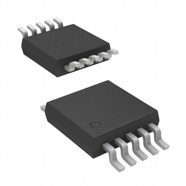
| 产品图片 |
|
| rohs | 符合RoHS无铅 / 符合限制有害物质指令(RoHS)规范要求 |
| 产品系列 | 电源管理 IC,开关控制器 ,Texas Instruments LM5020MMX-1/NOPB- |
| 数据手册 | |
| 产品型号 | LM5020MMX-1/NOPB |
| PWM类型 | 电流模式 |
| 上升时间 | 18 ns |
| 下降时间 | 15 ns |
| 产品 | Current Mode PWM Controllers |
| 产品种类 | 开关控制器 |
| 倍增器 | 无 |
| 关闭 | Yes |
| 其它名称 | 296-35291-6 |
| 分频器 | 无 |
| 包装 | Digi-Reel® |
| 升压 | 是 |
| 占空比 | 85% |
| 占空比-最大 | 80 % |
| 参考设计库 | http://www.digikey.com/rdl/4294959904/4294959903/255 |
| 反向 | 是 |
| 反激式 | 是 |
| 同步管脚 | No |
| 商标 | Texas Instruments |
| 安装风格 | SMD/SMT |
| 封装 | Reel |
| 封装/外壳 | 10-TFSOP,10-MSOP(0.118",3.00mm 宽) |
| 封装/箱体 | VSSOP-10 |
| 工作温度 | -40°C ~ 125°C |
| 工作电源电压 | 13 V to 90 V |
| 工作电源电流 | 3 mA |
| 工厂包装数量 | 3500 |
| 开关频率 | 200 kHz,630 kHz |
| 拓扑结构 | Divider |
| 描述/功能 | High voltage pulse-width-modulation controller |
| 最大工作温度 | + 125 C |
| 最小工作温度 | - 40 C |
| 标准包装 | 1 |
| 电压-电源 | 13 V ~ 90 V |
| 类型 | Current Mode PWM Controller |
| 系列 | LM5020 |
| 绝缘 | Non-Isolated |
| 设计资源 | http://www.digikey.com/product-highlights/cn/zh/texas-instruments-webench-design-center/3176 |
| 输入电压 | 100 V |
| 输出数 | 1 |
| 输出电压 | 8 V to 15 V |
| 输出电流 | 1 A |
| 输出端数量 | 1 Output |
| 配用 | /product-detail/zh/LM5020EVAL/LM5020EVAL-ND/695389/product-detail/zh/LM5020EVAL%2FNOPB/LM5020EVAL%2FNOPB-ND/2753639 |
| 降压 | 是 |
| 隔离式 | 无 |
| 频率-最大值 | 1MHz |


- 商务部:美国ITC正式对集成电路等产品启动337调查
- 曝三星4nm工艺存在良率问题 高通将骁龙8 Gen1或转产台积电
- 太阳诱电将投资9.5亿元在常州建新厂生产MLCC 预计2023年完工
- 英特尔发布欧洲新工厂建设计划 深化IDM 2.0 战略
- 台积电先进制程称霸业界 有大客户加持明年业绩稳了
- 达到5530亿美元!SIA预计今年全球半导体销售额将创下新高
- 英特尔拟将自动驾驶子公司Mobileye上市 估值或超500亿美元
- 三星加码芯片和SET,合并消费电子和移动部门,撤换高东真等 CEO
- 三星电子宣布重大人事变动 还合并消费电子和移动部门
- 海关总署:前11个月进口集成电路产品价值2.52万亿元 增长14.8%


PDF Datasheet 数据手册内容提取
LM5020 www.ti.com SNVS275F–MAY2004–REVISEDAPRIL2006 LM5020 100V Current Mode PWM Controller CheckforSamples:LM5020 FEATURES PACKAGES 1 • InternalStart-upBiasRegulator • VSSOP-10 2 • ErrorAmplifier • WSON-10(4mmx4mm) • PrecisionVoltageReference DESCRIPTION • ProgrammableSoftstart The LM5020 high voltage pulse-width-modulation • 1APeakGateDriver (PWM) controller contains all of the features needed • MaximumDutyCycleLimiting(80%for to implement single ended primary power converter LM5020-1or50%forLM5020-2) topologies. Output voltage regulation is based on • ProgrammableLineUnderVoltageLockout current-mode control, which eases the design of loop compensation while providing inherent line feed- (UVLO)withAdjustableHysteresis forward. The LM5020 includes a high-voltage start-up • Cycle-by-CycleOver-CurrentProtection regulator that operates over a wide input range up to • SlopeCompensation(LM5020-1) 100V. The PWM controller is designed for high speed • ProgrammableOscillatorFrequencywith capability including an oscillator frequency range to 1MHz and total propagation delays less than 100ns. SynchronizationCapability Additional features include an error amplifier, • CurrentSenseLeadingEdgeBlanking precision reference, line under-voltage lockout, cycle- • ThermalShutdownProtection by-cycle current limit, slope compensation, softstart, oscillator synchronization capability and thermal APPLICATIONS shutdown. The controller is available in both VSSOP- 10andWSON-10packages. • TelecommunicationPowerConverters • IndustrialPowerConverters • +42VAutomotiveSystems Typical Application Circuit V IN VIN VCC VOUT LM5020 UVLO SS OUT CS RT/SYNC FB GND COMP COMPENSATION Figure1. Non-IsolatedFlybackConverter 1 Pleasebeawarethatanimportantnoticeconcerningavailability,standardwarranty,anduseincriticalapplicationsof TexasInstrumentssemiconductorproductsanddisclaimerstheretoappearsattheendofthisdatasheet. Alltrademarksarethepropertyoftheirrespectiveowners. 2 PRODUCTIONDATAinformationiscurrentasofpublicationdate. Copyright©2004–2006,TexasInstrumentsIncorporated Products conform to specifications per the terms of the Texas Instruments standard warranty. Production processing does not necessarilyincludetestingofallparameters.
LM5020 SNVS275F–MAY2004–REVISEDAPRIL2006 www.ti.com Connection Diagram TopView 1 10 VIN SS 2 9 FB RT/SYNC 3 8 COMP CS 4 7 VCC UVLO 5 6 OUT GND Figure2. 10-LeadVSSOP,WSON PINDESCRIPTIONS Pin Name Description ApplicationInformation 1 VIN SourceInputVoltage Inputtothestart-upregulator.Inputrangeis13Vto100V. 2 FB FeedbackSignal Invertinginputoftheinternalerroramplifier.Thenon- invertinginputisinternallyconnectedtoa1.25Vreference. 3 COMP Theoutputoftheerroramplifierandinputtothe COMPpull-upisprovidedbyaninternal5Kresistorwhich PulseWidthModulator maybeusedtobiasanopto-couplertransistor. 4 VCC Outputoftheinternalhighvoltageseriespass Ifanauxiliarywindingraisesthevoltageonthispinabove regulator.Regulatedoutputvoltageis7.7V theregulationsetpoint,theinternalseriespassregulator willshutdown,reducingtheinternalpowerdissipation. 5 OUT OutputofthePWMcontroller Gatedriveroutputwitha1Apeakcurrentcapability. 6 GND Groundreturn 7 UVLO LineUnder-VoltageShutdown Anexternalresistordividerfromthepowerconverter sourcevoltagesetstheshutdownlevels.Thethresholdat thispinis1.25V.Hysteresisissetbyaswitchedinternal 20µAcurrentsource. 8 CS CurrentSenseinput Currentsenseinputforcurrentmodecontrolandover- currentprotection.Currentlimitingisaccomplishedusinga dedicatedcurrentsensecomparator.IftheCSpinvoltage exceeds0.5VtheOUTpinswitcheslowforcycle-by-cycle currentlimiting.CSisheldlowfor50nsafterOUTswitches hightoblankleadingedgecurrentspikes. 9 RT/SYNC Oscillatortimingresistorpinandsynchronization AnexternalresistorconnectedfromRTtoGNDsetsthe input oscillatorfrequency.Thispinalsoacceptssynchronization pulsesfromanexternalclock. 10 SS SoftstartInput Anexternalcapacitorandaninternal10µAcurrentsource setthesoft-startramprate. Thesedeviceshavelimitedbuilt-inESDprotection.Theleadsshouldbeshortedtogetherorthedeviceplacedinconductivefoam duringstorageorhandlingtopreventelectrostaticdamagetotheMOSgates. 2 SubmitDocumentationFeedback Copyright©2004–2006,TexasInstrumentsIncorporated ProductFolderLinks:LM5020
LM5020 www.ti.com SNVS275F–MAY2004–REVISEDAPRIL2006 Absolute Maximum Ratings(1)(2) VINtoGND -0.3Vto100V VCCtoGND -0.3Vto16V RTtoGND -0.3Vto5.5V AllotherpinstoGND -0.3Vto7V PowerDissipation InternallyLimited ESDRating(3) HumanBodyModel 2kV StorageTemperature -65°Cto+150°C JunctionTemperature 150°C (1) AbsoluteMaximumRatingsarelimitsbeyondwhichdamagetothedevicemayoccur.OperatingRatingsareconditionsunderwhich operationofthedeviceisintendedtobefunctional.Forensuredspecificationsandtestconditions,seetheElectricalCharacteristics. (2) IfMilitary/Aerospacespecifieddevicesarerequired,pleasecontacttheTexasInstrumentsSalesOffice/Distributorsforavailabilityand specifications. (3) Thehumanbodymodelisa100pFcapacitordischargedthrougha1.5kΩresistor. Operating Ratings VINVoltage 13Vto90V ExternalVoltageappliedtoVCC 8Vto15V OperatingJunctionTemperature -40°Cto+125°C Electrical Characteristics SpecificationsinstandardtypefaceareforT=+25°Candthoseinboldfacetypeapplyoverthefulloperatingjunction J temperaturerange.Unlessotherwisespecified:VIN=48V,VCC=10V,andRT=31.6kΩ.(1) Symbol Parameter Conditions Min Typ Max Units StartupRegulator V Reg V Regulation V =Open 7.4 7.7 8.0 V CC CC CC V CurrentLimit See(2) 15 22 mA CC I-V StartupRegulatorLeakage V =100V 150 500 µA IN IN I ShutdownCurrent V =0V,V =open 250 350 µA IN UVLO CC VCCSupply V UVLO(Rising) VccReg VccReg- V CC -300mV 100mV V UVLO(Falling) 5.3 6.0 6.7 V CC I SupplyCurrent Cload=0 2 3 mA CC ErrorAmplifier GBW GainBandwidth 4 MHz DCGain 75 dB ReferenceVoltage FB=COMP 1.225 1.25 1.275 V COMPSinkCapability FB=1.5VCOMP=1V 5 17 mA UVLOPin ShutdownThreshold 1.225 1.25 1.275 V UndervoltageShutdownHysteresis 16 20 24 µA CurrentSource CurrentLimit ILIMDelaytoOutput CSstepfrom0to0.6V 30 ns TimetoonsetofOUT Transition(90%) CyclebyCycleCSThreshold 0.45 0.5 0.55 V Voltage LeadingEdgeBlankingTime 50 ns (1) Limitsare100%productiontestedat25°C.Limitsovertheoperatingtemperaturerangearespecifiedthroughcorrelationusing StatisticalQualityControl(SQC)methods.ThelimitsareusedtocalculateNational'sAverageOutgoingQualityLevel(AOQL). (2) Devicethermallimitationsmaylimitusablerange. Copyright©2004–2006,TexasInstrumentsIncorporated SubmitDocumentationFeedback 3 ProductFolderLinks:LM5020
LM5020 SNVS275F–MAY2004–REVISEDAPRIL2006 www.ti.com Electrical Characteristics (continued) SpecificationsinstandardtypefaceareforT=+25°Candthoseinboldfacetypeapplyoverthefulloperatingjunction J temperaturerange.Unlessotherwisespecified:VIN=48V,VCC=10V,andRT=31.6kΩ.(1) Symbol Parameter Conditions Min Typ Max Units CSSinkImpedance(clocked) 35 55 Ω SoftStart SoftstartCurrentSource 7 10 13 µA SoftstarttoCOMPOffset 0.35 0.55 0.75 V Oscillator Frequency1(RT=31.6k) See(3) 175 200 225 kHz Frequency2(RT=9.76k) See(3) 560 630 700 kHz Syncthreshold 2.4 3.2 3.8 V PWMComparator DelaytoOutput COMPsetto2V, 25 ns CSstepped0to0.4V, TimetoonsetofOUT transitionlow MinDutyCycle COMP=0V 0 % MaxDutyCycle(-1Device) 75 80 85 % MaxDutyCycle(-2Device) 50 % COMPtoPWMComparatorGain 0.33 COMPOpenCircuitVoltage 4.3 5.2 6.1 V COMPShortCircuitCurrent COMP=0V 0.6 1.1 1.5 mA SlopeCompensation SlopeCompAmplitude DeltaincreaseatPWM 80 105 130 mV (LM5020-1DeviceOnly) ComparatortoCS OutputSection OutputHighSaturation Iout=50mA,V -V 0.25 0.75 V CC OUT OutputLowSaturation I =100mA,V 0.25 0.75 V OUT OUT RiseTime Cload=1nF 18 ns FallTime Cload=1nF 15 ns ThermalShutdown Tsd ThermalShutdownTemp. 165 °C ThermalShutdownHysteresis 25 °C (3) Specificationappliestotheoscillatorfrequency.TheoperationalfrequencyoftheLM5020-2devicesisdividedbytwo. 4 SubmitDocumentationFeedback Copyright©2004–2006,TexasInstrumentsIncorporated ProductFolderLinks:LM5020
LM5020 www.ti.com SNVS275F–MAY2004–REVISEDAPRIL2006 Typical Performance Characteristics Unlessotherwisespecified:T =25°C. J V andV V CC IN CC vs vs V I (V =48V) 20 IN 9 CC IN 18 8 16 7 14 6 12 V) V) V(CC 180 V (CC 45 6 3 4 2 2 0 1 0 10 20 0 5 10 15 20 25 VIN (V) ICC (mA) Figure3. Figure4. OscillatorFrequency OscillatorFrequency vs vs Temperature RT RT=31.6kΩ 1.00E+06 210 205 z) UENCY (Hz) 1.00E+05 ENCY (kH 200 Q U FRE REQ F 195 1.00E+04 190 1 10 100 -40 10 60 110 RT (k:) TEMPERATURE (oC) Figure5. Figure6. SoftStartCurrent vs Temperature ErrorAmp.Gain/PhasePlot 13.0 50 225 40 180 11.8 30 135 20 90 A) RENT (P 10.6 )Bd( NIA 100 405 o) E(SAH R 9.4 G -10 -45 P U C -20 -90 8.2 -30 -135 -40 -180 7.0 -50 -225 -40 10 60 110 10k 100k 1M 10M TEMPERATURE (oC) FREQUEN CY (Hz) Figure7. Figure8. Copyright©2004–2006,TexasInstrumentsIncorporated SubmitDocumentationFeedback 5 ProductFolderLinks:LM5020
LM5020 SNVS275F–MAY2004–REVISEDAPRIL2006 www.ti.com Block Diagram 7.7V SERIES REGULATOR VIN VCC 5V REFERENCE 1.25V ENABLE UVLO + - LOGIC 1.25V UVLO HYSTERESIS (20 PA) CLK RT/SYNC OSC VCC DRIVER SLOPECOMP OUT RAMP 50 PA Max Duty Limit S Q GENERATOR LM5020-1 (80%) (LM5020-1 Only) 0 LM5020-2 (50%) R Q 5V COMP GND 1.25V 5k PWM 2R + FB - LOGIC 1.4V R SS SS 10 PA CS SS + 2k 0.5V - CLK + LEB 6 SubmitDocumentationFeedback Copyright©2004–2006,TexasInstrumentsIncorporated ProductFolderLinks:LM5020
LM5020 www.ti.com SNVS275F–MAY2004–REVISEDAPRIL2006 DETAILED OPERATING DESCRIPTION The LM5020 High Voltage PWM controller contains all of the features needed to implement single ended primary power converter topologies. The LM5020 includes a high-voltage startup regulator that operates over a wide input range to 100V. The PWM controller is designed for high speed capability including an oscillator frequency range to 1MHz and total propagation delays less than 100ns. Additional features include an error amplifier, precision reference, line under-voltage lockout, cycle-by-cycle current limit, slope compensation, softstart, oscillator sync capability and thermal shutdown. The functional block diagram of the LM5020 is shown in Figure 1. The LM5020 is designed for current-mode control power converters, which require a single drive output, such as Flyback and Forward topologies. The LM5020 provides all of the advantages of current-mode control includinglinefeed-forward,cycle-by-cyclecurrentlimitingandsimplifiedloopcompensation. High Voltage Start-Up Regulator The LM5020 contains an internal high voltage startup regulator, that allows the input pin (Vin) to be connected directly to line voltages as high as 100V. The regulator output is internally current limited to 15mA. When power is applied, the regulator is enabled and sources current into an external capacitor connected to the V pin. The CC recommended capacitance range for the Vcc regulator is 0.1µF to 100µF. When the voltage on the V pin CC reaches the regulation level of 7.7V, the controller output is enabled. The controller will remain enabled until V CC fallsbelow6V. In typical applications, a transformer auxiliary winding is connected through a diode to the V pin. This winding CC should raise the V voltage above 8V to shut off the internal startup regulator. Powering V from an auxiliary CC CC winding improves conversion efficiency while reducing the power dissipated in the controller. The external V CC capacitor must be selected such that the capacitor maintains the Vcc voltage greater than the V UVLO falling CC threshold (6V) during the initial start-up. During a fault condition when the converter auxiliary winding is inactive, external current draw on the V line should be limited such that the power dissipated in the start-up regulator CC doesnotexceedthemaximumpowerdissipationcapabilityofthecontroller. An external start-up or other bias rail can be used instead of the internal start-up regulator by connecting the V CC andtheVinpinstogetherandfeedingtheexternalbiasvoltage(8-15V)tothetwopins. Line Under Voltage Detector The LM5020 contains a line Under Voltage Lock Out (UVLO) circuit. An external set-point voltage divider from Vin to GND sets the operational range of the converter. The resistor divider must be designed such that the voltage at the UVLO pin is greater than 1.25V when Vin is in the desired operating range. If the under voltage threshold is not met, all functions of the controller are disabled and the controller remains in a low power standby state. UVLO hysteresis is accomplished with an internal 20µA current source that is switched on or off into the impedance of the set-point divider. When the UVLO threshold is exceeded, the current source is activated to instantly raise the voltage at the UVLO pin. When the UVLO pin voltage falls below the 1.25V threshold the current source is turned off, causing the voltage at the UVLO pin to fall. The UVLO pin can also be used to implement a remote enable / disable function. If an external transistor pulls the UVLO pin below the 1.25V threshold,theconverterisdisabled. Error Amplifier An internal high gain error amplifier is provided within the LM5020. The amplifier's non-inverting input is internally set to a fixed reference voltage of 1.25V. The inverting input is connected to the FB pin. In non-isolated applications, the power converter output is connected to the FB pin via voltage scaling resistors. Loop compensation components are connected between the COMP and FB pins. For most isolated applications the error amplifier function is implemented on the secondary side of the converter and the internal error amplifier is not used. The internal error amplifier is configured as an open drain output and can be disabled by connecting theFBpintoground.Aninternal5Kpull-upresistorbetweena5VreferenceandCOMPcanbeusedasthepull- upforanoptocouplerinisolatedapplications. Copyright©2004–2006,TexasInstrumentsIncorporated SubmitDocumentationFeedback 7 ProductFolderLinks:LM5020
LM5020 SNVS275F–MAY2004–REVISEDAPRIL2006 www.ti.com Current Limit/Current Sense The LM5020 provides a cycle-by-cycle over current protection function. Current limit is accomplished by an internal current sense comparator. If the voltage at the current sense comparator input exceeds 0.5V, the output is immediately terminated. A small RC filter, located near the controller, is recommended to filter noise from the current sense signal. The CS input has an internal MOSFET which discharges the CS pin capacitance at the conclusion of every cycle. The discharge device remains on an additional 50ns after the beginning of the new cycletoattenuatetheleadingedgespikeonthecurrentsensesignal. The LM5020 current sense and PWM comparators are very fast, and may respond to short duration noise pulses. Layout considerations are critical for the current sense filter and sense resistor. The capacitor associated with the CS filter must be located very close to the LM5020 and connected directly to the pins of the controller (CS and GND). If a current sense transformer is used, both leads of the transformer secondary should be routed to the sense resistor and the current sense filter network. A sense resistor located in the source of the primary power MOSFET may be used for current sensing, but a low inductance resistor is required. When designing with a current sense resistor all of the noise sensitive low power ground connections should be connected together local to the controller and a single connection should be made to the high current power ground (sense resistor groundpoint). Oscillator and Sync Capability A single external resistor connected between the RT and GND pins sets the LM5020 oscillator frequency. Internal to the LM5020-2 device (50% duty cycle limited option) is an oscillator divide by two circuit. This divide by two circuit creates an exact 50% duty cycle pulse which is used internally to create a precise 50% duty cycle limit function. Because of this, the internal oscillator actually operates at twice the frequency of the output (OUT). For the LM5020-1 device the oscillator frequency and the operational output frequency are the same. To set a desiredoutputoperationalfrequency(F),theRTresistorcanbecalculatedfrom: LM5020-1: 1 RT = F x 158 x 10-12 (1) LM5020-2: 1 RT = F x 316 x 10-12 (2) The LM5020 can also be synchronized to an external clock. The external clock must have a higher frequency than the free running oscillator frequency set by the RT resistor. The clock signal should be capacitively coupled into the RT pin through a 100pF capacitor. A peak voltage level greater than 3.7 Volts at the RT pin is required for detection of the sync pulse. The sync pulse width should be set between 15 to 150ns by the external components.TheRTresistorisalwaysrequired,whethertheoscillatorisfreerunningorexternallysynchronized. The voltage at the RT pin is internally regulated at 2 Volts. The RT resistor should be located very close to the deviceandconnecteddirectlytothepinsofthecontroller(RTandGND). PWM Comparator / Slope Compensation The PWM comparator compares the current ramp signal with the loop error voltage derived from the error amplifier output. The error amplifier output voltage at the COMP pin is offset by 1.4V and then further attenuated by a 3:1 resistor divider. The PWM comparator polarity is such that 0 Volts on the COMP pin will result in a zero duty cycle at the controller output. For duty cycles greater than 50 percent, current mode control circuits are subjecttosub-harmonicoscillation.Byaddinganadditionalfixedslopevoltagerampsignal(slopecompensation) to the current sense signal, this oscillation can be avoided. The LM5020-1 integrates this slope compensation by summing a current ramp generated by the oscillator with the current sense signal. Additional slope compensation may be added by increasing the source impedance of the current sense signal. Since the LM5020-2 is not capableofdutycyclesgreaterthan50%,thereisnoslopecompensationfeatureinthisdevice. 8 SubmitDocumentationFeedback Copyright©2004–2006,TexasInstrumentsIncorporated ProductFolderLinks:LM5020
LM5020 www.ti.com SNVS275F–MAY2004–REVISEDAPRIL2006 Soft Start Thesoftstartfeatureallowsthepowerconvertertograduallyreachtheinitialsteadystateoperatingpoint,thereby reducing start-up stresses and current surges. At power on, after the V and the line undervoltage lockout CC thresholds are satisfied, an internal 10µA current source charges an external capacitor connected to the SS pin. The capacitor voltage will ramp up slowly and will limit the COMP pin voltage and the duty cycle of the output pulses. Gate Driver and Maximum Duty Cycle Limit The LM5020 provides an internal gate driver (OUT), which can source and sink a peak current of 1 Amp. The LM5020 is available in two duty cycle limit options. The maximum output duty cycle is typically 80% for the LM5020-1 option and precisely equal to 50% for the LM5020-2 option. The maximum duty cycle function for the LM5020-2 is accomplished with an internal toggle flip-flop which ensures an accurate duty cycle limit. The internal oscillator frequency of the LM5020-2 is therefore twice the operating frequency of the PWM controller (OUTpin). The 80% maximum duty cycle limit of the LM5020-1 is determined by the internal oscillator and varies more than the 50% limit of the LM5020-2. For the LM5020-1 the internal oscillator frequency and the operational frequency ofthePWMcontrollerareequal. Thermal Protection Internal thermal shutdown circuitry is provided to protect the integrated circuit in the event the maximum junction temperature is exceeded. This feature prevents catastrophic failures from accidental device overheating. When activated, typically at 165 degrees Celsius, the controller is forced into a low power standby state, disabling the output driver and the bias regulator. After the temperature is reduced (typical hysteresis = 25°C) the V CC regulatorisenabledandasoftstartsequenceinitiated. Typical Application Circuit: 36V - 75 V and 3.3V, 4.5A OUT IN C12 J2 R13 R10 470 pF +3.3V C9 2 J1 V+ T1 30-75V IN 0.1 PF 20 D2 10, 1W 1 1 CMPD2838E C13 C14 C15 GND 100 PF 100 PF 270 PF OUT RTN D3 2 GND MBRD835L GND GND GND GND R2 R1 GND C1 C2 61.9k 10 GND Z1 2.2 PF 2.2 PF 1SMB5936B GND GND GND D1 C4 C10 CMPD2838E Shutdown 0.1 PF 4.7 PF 5678 R3 GND GND 0.0C13 PF 2.87k R1.400k 1U1 4 QSi17898DP R2.1413k VIN VCC 7 GND GND UVLO 5 4321 OUT R12 3 COMP 8 R7 1.47k SYNC 9 RT/ CS 2 Input C8 10 SYNC FB 6 100R8 R9 100 pF SS GND 0.47 0.47 GND R5 R6 LM5020 C11 C6 15.0k 12.4k 1000 pF 220 pF C5 C7 0.01 PF GND GND GND 3300 pF GND GND Copyright©2004–2006,TexasInstrumentsIncorporated SubmitDocumentationFeedback 9 ProductFolderLinks:LM5020
LM5020 SNVS275F–MAY2004–REVISEDAPRIL2006 www.ti.com Table1.BillOfMaterials ITEM PARTNUMBER DESCRIPTION VALUE C 1 C4532X7R2A225M CAPACITOR,CER,TDK 2.2µF,100V C 2 C4532X7R2A225M CAPACITOR,CER,TDK 2.2µF,100V C 3 C2012X7R1H103K CAPACITOR,CER,TDK 0.01µF,50V C 4 C3216X7R2A104K CAPACITOR,CER,TDK 0.1µF,100V C 5 C2012X7R1H103K CAPACITOR,CER,TDK 0.01µF,50V C 6 C2012C0G1H221J CAPACITOR,CER,KEMET 220pF,50V C 7 C2012C0G1H332J CAPACITOR,CER,TDK 3300pF,50V C 8 C2012C0G1H101J CAPACITOR,CER,TDK 100pF,50V C 9 C2012X7R1H104K CAPACITOR,CER,TDK 0.1µF,50V C 10 C3216X7R1C475K CAPACITOR,CER,TDK 4.7µF,16V C 11 C2012C0G1H102J CAPACITOR,CER,TDK 1000pF,50V C 12 C2012C0G1H471J CAPACITOR,CER,TDK 470p,50V C 13 C4532X7S0G107M CAPACITOR,CER,TDK 100µF,4V C 14 C4532X7S0G107M CAPACITOR,CER,TDK 100µF,4V C 15 A700X277M0004AT CAPACITOR,ALUMORGANIC,KEMET 270µF,4V D 1 CMPD2838E-NSA DIODE,SIGNAL,CENTRAL D 2 CMPD2838E-NSA DIODE,SIGNAL,CENTRAL D 3 MBRD835L DIODE,RECTIFIER,ON SEMICONDUCTOR J 1 MKDS1/2-3.81 TERMBLK,MINI,2POS,PHOENIX CONTACT J 2 MKDS1/2-3.81 TERMBLK,MINI,2POS,PHOENIX CONTACT Q 1 SI7898DP FET,SILICONIX 150V,85mΩ R 1 CRCW120610R0F RESISTOR 10 R 2 CRCW12066192F RESISTOR 61.9kΩ R 3 CRCW08052871F RESISTOR 2.87kΩ R 4 CRCW08051001F RESISTOR 1.00kΩ R 5 CRCW08051502F RESISTOR 15.0kΩ R 6 CRCW08051242F RESISTOR 12.4kΩ R 7 CRCW08051000F RESISTOR 100 R 8 CRCW12060R47F RESISTOR 0.47 R 9 CRCW12060R47F RESISTOR 0.47 R 10 CRCW251210R0F RESISTOR 10,1W R 11 CRCW08052431F RESISTOR 2.43K R 12 CRCW08051471F RESISTOR 1.47K R 13 CRCW080520R0F RESISTOR 20 T 1 B0695-ACOILCRAFT TRANSFORMER,FLYBACK,EFD20CORE T 1 PA0751PULSE TRANSFORMER,FLYBACK,EFD20CORE ALTERNATE U 1 LM5020-2MM CONTROLLER,SINGLEOUT,PWM, NATIONAL Z 1 1SMB5936B DIODE,ZENER,SMB,30V 10 SubmitDocumentationFeedback Copyright©2004–2006,TexasInstrumentsIncorporated ProductFolderLinks:LM5020
PACKAGE OPTION ADDENDUM www.ti.com 6-Feb-2020 PACKAGING INFORMATION Orderable Device Status Package Type Package Pins Package Eco Plan Lead/Ball Finish MSL Peak Temp Op Temp (°C) Device Marking Samples (1) Drawing Qty (2) (6) (3) (4/5) LM5020MM-1 NRND VSSOP DGS 10 1000 TBD Call TI Call TI -40 to 125 SBLB LM5020MM-1/NOPB ACTIVE VSSOP DGS 10 1000 Green (RoHS SN Level-1-260C-UNLIM -40 to 125 SBLB & no Sb/Br) LM5020MM-2/NOPB ACTIVE VSSOP DGS 10 1000 Green (RoHS SN Level-1-260C-UNLIM -40 to 125 SBNB & no Sb/Br) LM5020MMX-1/NOPB ACTIVE VSSOP DGS 10 3500 Green (RoHS SN Level-1-260C-UNLIM -40 to 125 SBLB & no Sb/Br) LM5020MMX-2/NOPB ACTIVE VSSOP DGS 10 3500 Green (RoHS SN Level-1-260C-UNLIM -40 to 125 SBNB & no Sb/Br) LM5020SD-1/NOPB ACTIVE WSON DPR 10 1000 Green (RoHS SN Level-1-260C-UNLIM -40 to 125 5020-1 & no Sb/Br) LM5020SD-2/NOPB ACTIVE WSON DPR 10 1000 Green (RoHS SN Level-1-260C-UNLIM -40 to 125 5020-2 & no Sb/Br) LM5020SDX-1/NOPB ACTIVE WSON DPR 10 4500 Green (RoHS SN Level-1-260C-UNLIM -40 to 125 5020-1 & no Sb/Br) LM5020SDX-2/NOPB ACTIVE WSON DPR 10 4500 Green (RoHS SN Level-1-260C-UNLIM -40 to 125 5020-2 & no Sb/Br) (1) The marketing status values are defined as follows: ACTIVE: Product device recommended for new designs. LIFEBUY: TI has announced that the device will be discontinued, and a lifetime-buy period is in effect. NRND: Not recommended for new designs. Device is in production to support existing customers, but TI does not recommend using this part in a new design. PREVIEW: Device has been announced but is not in production. Samples may or may not be available. OBSOLETE: TI has discontinued the production of the device. (2) RoHS: TI defines "RoHS" to mean semiconductor products that are compliant with the current EU RoHS requirements for all 10 RoHS substances, including the requirement that RoHS substance do not exceed 0.1% by weight in homogeneous materials. Where designed to be soldered at high temperatures, "RoHS" products are suitable for use in specified lead-free processes. TI may reference these types of products as "Pb-Free". RoHS Exempt: TI defines "RoHS Exempt" to mean products that contain lead but are compliant with EU RoHS pursuant to a specific EU RoHS exemption. Green: TI defines "Green" to mean the content of Chlorine (Cl) and Bromine (Br) based flame retardants meet JS709B low halogen requirements of <=1000ppm threshold. Antimony trioxide based flame retardants must also meet the <=1000ppm threshold requirement. (3) MSL, Peak Temp. - The Moisture Sensitivity Level rating according to the JEDEC industry standard classifications, and peak solder temperature. (4) There may be additional marking, which relates to the logo, the lot trace code information, or the environmental category on the device. Addendum-Page 1
PACKAGE OPTION ADDENDUM www.ti.com 6-Feb-2020 (5) Multiple Device Markings will be inside parentheses. Only one Device Marking contained in parentheses and separated by a "~" will appear on a device. If a line is indented then it is a continuation of the previous line and the two combined represent the entire Device Marking for that device. (6) Lead/Ball Finish - Orderable Devices may have multiple material finish options. Finish options are separated by a vertical ruled line. Lead/Ball Finish values may wrap to two lines if the finish value exceeds the maximum column width. Important Information and Disclaimer:The information provided on this page represents TI's knowledge and belief as of the date that it is provided. TI bases its knowledge and belief on information provided by third parties, and makes no representation or warranty as to the accuracy of such information. Efforts are underway to better integrate information from third parties. TI has taken and continues to take reasonable steps to provide representative and accurate information but may not have conducted destructive testing or chemical analysis on incoming materials and chemicals. TI and TI suppliers consider certain information to be proprietary, and thus CAS numbers and other limited information may not be available for release. In no event shall TI's liability arising out of such information exceed the total purchase price of the TI part(s) at issue in this document sold by TI to Customer on an annual basis. Addendum-Page 2
PACKAGE MATERIALS INFORMATION www.ti.com 29-Sep-2019 TAPE AND REEL INFORMATION *Alldimensionsarenominal Device Package Package Pins SPQ Reel Reel A0 B0 K0 P1 W Pin1 Type Drawing Diameter Width (mm) (mm) (mm) (mm) (mm) Quadrant (mm) W1(mm) LM5020MM-1 VSSOP DGS 10 1000 178.0 12.4 5.3 3.4 1.4 8.0 12.0 Q1 LM5020MM-1/NOPB VSSOP DGS 10 1000 178.0 12.4 5.3 3.4 1.4 8.0 12.0 Q1 LM5020MM-2/NOPB VSSOP DGS 10 1000 178.0 12.4 5.3 3.4 1.4 8.0 12.0 Q1 LM5020MMX-1/NOPB VSSOP DGS 10 3500 330.0 12.4 5.3 3.4 1.4 8.0 12.0 Q1 LM5020MMX-2/NOPB VSSOP DGS 10 3500 330.0 12.4 5.3 3.4 1.4 8.0 12.0 Q1 LM5020SD-1/NOPB WSON DPR 10 1000 178.0 12.4 4.3 4.3 1.3 8.0 12.0 Q1 LM5020SD-2/NOPB WSON DPR 10 1000 178.0 12.4 4.3 4.3 1.3 8.0 12.0 Q1 LM5020SDX-1/NOPB WSON DPR 10 4500 330.0 12.4 4.3 4.3 1.3 8.0 12.0 Q1 LM5020SDX-2/NOPB WSON DPR 10 4500 330.0 12.4 4.3 4.3 1.3 8.0 12.0 Q1 PackMaterials-Page1
PACKAGE MATERIALS INFORMATION www.ti.com 29-Sep-2019 *Alldimensionsarenominal Device PackageType PackageDrawing Pins SPQ Length(mm) Width(mm) Height(mm) LM5020MM-1 VSSOP DGS 10 1000 210.0 185.0 35.0 LM5020MM-1/NOPB VSSOP DGS 10 1000 210.0 185.0 35.0 LM5020MM-2/NOPB VSSOP DGS 10 1000 210.0 185.0 35.0 LM5020MMX-1/NOPB VSSOP DGS 10 3500 367.0 367.0 35.0 LM5020MMX-2/NOPB VSSOP DGS 10 3500 367.0 367.0 35.0 LM5020SD-1/NOPB WSON DPR 10 1000 210.0 185.0 35.0 LM5020SD-2/NOPB WSON DPR 10 1000 210.0 185.0 35.0 LM5020SDX-1/NOPB WSON DPR 10 4500 367.0 367.0 35.0 LM5020SDX-2/NOPB WSON DPR 10 4500 367.0 367.0 35.0 PackMaterials-Page2
PACKAGE OUTLINE DGS0010A VSSOP - 1.1 mm max height SCALE 3.200 SMALL OUTLINE PACKAGE C 5.05 4.75 TYP SEATING PLANE A PIN 1 ID 0.1 C AREA 8X 0.5 10 1 3.1 2X 2.9 NOTE 3 2 5 6 0.27 10X 0.17 B 3.1 0.1 C A B 1.1 MAX 2.9 NOTE 4 0.23 TYP SEE DETAIL A 0.13 0.25 GAGE PLANE 0.15 0.7 0 - 8 0.05 0.4 DETAIL A TYPICAL 4221984/A 05/2015 NOTES: 1. All linear dimensions are in millimeters. Any dimensions in parenthesis are for reference only. Dimensioning and tolerancing per ASME Y14.5M. 2. This drawing is subject to change without notice. 3. This dimension does not include mold flash, protrusions, or gate burrs. Mold flash, protrusions, or gate burrs shall not exceed 0.15 mm per side. 4. This dimension does not include interlead flash. Interlead flash shall not exceed 0.25 mm per side. 5. Reference JEDEC registration MO-187, variation BA. www.ti.com
EXAMPLE BOARD LAYOUT DGS0010A VSSOP - 1.1 mm max height SMALL OUTLINE PACKAGE 10X (1.45) 10X (0.3) SYMM (R0.05) TYP 1 10 SYMM 8X (0.5) 5 6 (4.4) LAND PATTERN EXAMPLE SCALE:10X SOOPLEDNEINRG MASK METAL MSOELTDAEL RU NMDAESRK SOOPLEDNEINRG MASK 0.05 MAX 0.05 MIN ALL AROUND ALL AROUND NON SOLDER MASK SOLDER MASK DEFINED DEFINED SOLDER MASK DETAILS NOT TO SCALE 4221984/A 05/2015 NOTES: (continued) 6. Publication IPC-7351 may have alternate designs. 7. Solder mask tolerances between and around signal pads can vary based on board fabrication site. www.ti.com
EXAMPLE STENCIL DESIGN DGS0010A VSSOP - 1.1 mm max height SMALL OUTLINE PACKAGE 10X (1.45) SYMM (R0.05) TYP 10X (0.3) 1 10 SYMM 8X (0.5) 5 6 (4.4) SOLDER PASTE EXAMPLE BASED ON 0.125 mm THICK STENCIL SCALE:10X 4221984/A 05/2015 NOTES: (continued) 8. Laser cutting apertures with trapezoidal walls and rounded corners may offer better paste release. IPC-7525 may have alternate design recommendations. 9. Board assembly site may have different recommendations for stencil design. www.ti.com
MECHANICAL DATA DPR0010A SDC10A (Rev A) www.ti.com
IMPORTANTNOTICEANDDISCLAIMER TI PROVIDES TECHNICAL AND RELIABILITY DATA (INCLUDING DATASHEETS), DESIGN RESOURCES (INCLUDING REFERENCE DESIGNS), APPLICATION OR OTHER DESIGN ADVICE, WEB TOOLS, SAFETY INFORMATION, AND OTHER RESOURCES “AS IS” AND WITH ALL FAULTS, AND DISCLAIMS ALL WARRANTIES, EXPRESS AND IMPLIED, INCLUDING WITHOUT LIMITATION ANY IMPLIED WARRANTIES OF MERCHANTABILITY, FITNESS FOR A PARTICULAR PURPOSE OR NON-INFRINGEMENT OF THIRD PARTY INTELLECTUAL PROPERTY RIGHTS. These resources are intended for skilled developers designing with TI products. You are solely responsible for (1) selecting the appropriate TI products for your application, (2) designing, validating and testing your application, and (3) ensuring your application meets applicable standards, and any other safety, security, or other requirements. These resources are subject to change without notice. TI grants you permission to use these resources only for development of an application that uses the TI products described in the resource. Other reproduction and display of these resources is prohibited. No license is granted to any other TI intellectual property right or to any third party intellectual property right. TI disclaims responsibility for, and you will fully indemnify TI and its representatives against, any claims, damages, costs, losses, and liabilities arising out of your use of these resources. TI’s products are provided subject to TI’s Terms of Sale (www.ti.com/legal/termsofsale.html) or other applicable terms available either on ti.com or provided in conjunction with such TI products. TI’s provision of these resources does not expand or otherwise alter TI’s applicable warranties or warranty disclaimers for TI products. Mailing Address: Texas Instruments, Post Office Box 655303, Dallas, Texas 75265 Copyright © 2020, Texas Instruments Incorporated