ICGOO在线商城 > 集成电路(IC) > PMIC - 电源管理 - 专用 > LTC3589IUJ-1#PBF
/LTC3589IUJ-1#PBF.jpg)
 Datasheet下载
- 型号: LTC3589IUJ-1#PBF
- 制造商: LINEAR TECHNOLOGY
- 库位|库存: xxxx|xxxx
- 要求:
| 数量阶梯 | 香港交货 | 国内含税 |
| +xxxx | $xxxx | ¥xxxx |
查看当月历史价格
查看今年历史价格
LTC3589IUJ-1#PBF产品简介:
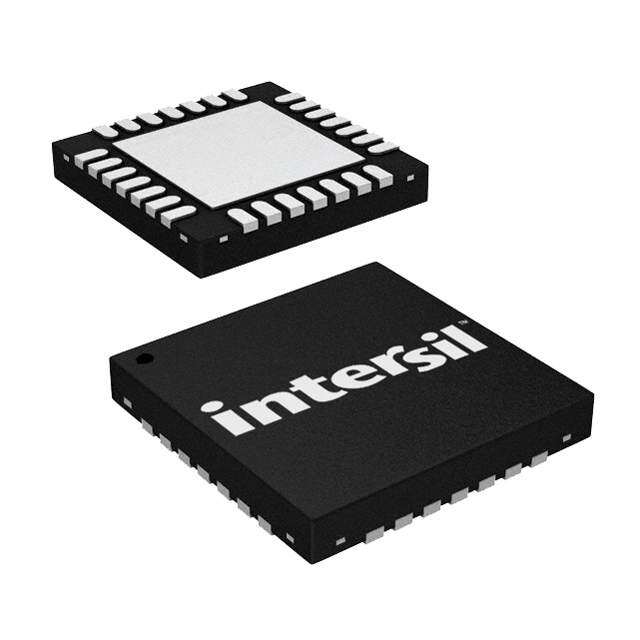
ICGOO电子元器件商城为您提供LTC3589IUJ-1#PBF由LINEAR TECHNOLOGY设计生产,在icgoo商城现货销售,并且可以通过原厂、代理商等渠道进行代购。 LTC3589IUJ-1#PBF价格参考。LINEAR TECHNOLOGYLTC3589IUJ-1#PBF封装/规格:PMIC - 电源管理 - 专用, 手持式/移动设备,OMAP™ PMIC 40-QFN(6x6)。您可以下载LTC3589IUJ-1#PBF参考资料、Datasheet数据手册功能说明书,资料中有LTC3589IUJ-1#PBF 详细功能的应用电路图电压和使用方法及教程。
LTC3589IUJ-1#PBF 是由 Linear Technology(现为 Analog Devices 旗下品牌)生产的一款高度集成的电源管理集成电路(PMIC),专为便携式和低功耗应用设计。该器件属于专用电源管理类别,广泛应用于需要多路电源轨管理的系统中。

主要应用场景包括:

1. 便携式医疗设备:如血糖仪、便携式监测设备等,LTC3589IUJ-1#PBF 可提供多路稳定电源,支持处理器、传感器和显示屏等模块的供电需求。

2. 工业手持设备:如数据采集器、便携式测试仪器,其高集成度和低静态电流特性有助于延长电池寿命并减小设备体积。

3. 电池供电系统:适用于锂离子电池供电的设备,能够高效管理电池能量,并支持多种电压轨输出,满足复杂系统的供电需求。

4. 嵌入式系统与FPGA电源管理:为低功耗FPGA、DSP或微处理器系统提供多路电源,支持上电时序控制,确保系统稳定启动。

5. 消费类电子产品:如电子书、便携式音频设备等,适用于对空间和功耗有严格要求的产品。

该芯片集成了多个DC/DC转换器、LDO、电池充电管理及电源路径管理功能,具有高集成度、低静态电流和灵活配置等优点,非常适合空间受限且需高效电源管理的场景。
| 参数 | 数值 |
| 产品目录 | 集成电路 (IC) |
| 描述 | IC CONV DC/DC 8-OUTPUT 40QFN |
| 产品分类 | |
| 品牌 | Linear Technology |
| 数据手册 | http://www.linear.com/docs/29451 |
| 产品图片 |
|
| 产品型号 | LTC3589IUJ-1#PBF |
| PCN设计/规格 | |
| rohs | 无铅 / 符合限制有害物质指令(RoHS)规范要求 |
| 产品系列 | - |
| 产品培训模块 | http://www.digikey.cn/PTM/IndividualPTM.page?site=cn&lang=zhs&ptm=25200 |
| 供应商器件封装 | 40-QFN(6x6) |
| 包装 | 管件 |
| 安装类型 | 表面贴装 |
| 封装/外壳 | 40-WFQFN 裸露焊盘 |
| 工作温度 | -40°C ~ 125°C |
| 应用 | 手持式/移动设备,OMAP™ |
| 标准包装 | 61 |
| 电压-电源 | 2.7 V ~ 5.5 V |
| 电流-电源 | 8µA |


- 商务部:美国ITC正式对集成电路等产品启动337调查
- 曝三星4nm工艺存在良率问题 高通将骁龙8 Gen1或转产台积电
- 太阳诱电将投资9.5亿元在常州建新厂生产MLCC 预计2023年完工
- 英特尔发布欧洲新工厂建设计划 深化IDM 2.0 战略
- 台积电先进制程称霸业界 有大客户加持明年业绩稳了
- 达到5530亿美元!SIA预计今年全球半导体销售额将创下新高
- 英特尔拟将自动驾驶子公司Mobileye上市 估值或超500亿美元
- 三星加码芯片和SET,合并消费电子和移动部门,撤换高东真等 CEO
- 三星电子宣布重大人事变动 还合并消费电子和移动部门
- 海关总署:前11个月进口集成电路产品价值2.52万亿元 增长14.8%


PDF Datasheet 数据手册内容提取
LTC3589/LTC3589-1/ LTC3589-2 8-Output Regulator with 2 Sequencing and I C FeaTures DescripTion n Triple I2C Adjustable High Efficiency Step-Down DC/ The LTC®3589 is a complete power management solu- DC Converters: 1.6A, 1A/1.2A, 1A/1.2A tion for ARM and ARM-based processors and advanced n High Efficiency 1.2A Buck-Boost DC/DC Converter portable microprocessor systems. The device contains n Triple 250mA LDO Regulators three step-down DC/DC converters for core, memory and n Pushbutton ON/OFF Control with System Reset SoC rails, a buck-boost regulator for I/O at 1.8V to 5V and n Flexible Pin-Strap Sequencing Operation three 250mA LDO regulators for low noise analog sup- n I2C and Independent Enable Control Pins plies. An I2C serial port is used to control enables, output n Power Good and Reset Outputs voltage levels, dynamic voltage scaling, operating modes n Dynamic Voltage Scaling and Slew Rate Control and status reporting. Differences between the LTC3589, n Selectable 2.25MHz or 1.12MHz Switching Frequency LTC3589-1, and LTC3589-2 are summarized in Table 1. n Always-Alive 25mA LDO Regulator Regulator start-up is sequenced by connecting outputs to n 8µA Standby Current enable pins in the desired order or programmed via the n 40-Pin 6mm × 6mm × 0.75mm QFN I2C port. System power-on, power-off, and reset functions are controlled by pushbutton interface, pin inputs, or I2C applicaTions interface. n Handheld Instruments and Scanners The LTC3589 supports i.MX53/51, PXA and OMAP pro- n Portable Industrial Devices cessors with eight independent rails at appropriate power n Automotive Infotainment levels. Other features include interface signals such as n Medical Devices the VSTB pin that simultaneously toggle up to four rails n High End Consumer Devices between programmed run and standby output voltages. n Multirail Systems The device is available in a low profile 40-pin 6mm × 6mm n Supports Freescale i.MX53/51, Marvell PXA and exposed pad QFN package. Other Application Processors L, LT, LTC, LTM, Burst Mode, Linear Technology and the Linear logo are registered trademarks of Linear Technology Corporation. All other trademarks are the property of their respective owners. Typical applicaTion VIN 2.7V TO 5.5V Start-Up Sequence VIN 1µH 0.8V TO VIN LDO1_STBY SW1 0.5V TO VIN AT 25mA AT 1.6A 1µF 22µF BB_OUT 1.5µH WAKE 0.36V TO VIN LDO2 SW2 0.5V TO VIN (1V/DIV) AT 250mA AT 1A 1µF LTC3589 22µF SW2 1.5µH 0.5V/DIV LDO3 1.8V LDO3 SW3 0.5V TO VIN AT 250mA AT 1A 1µF SW3 22µF LDO2 2.8V LDO4 2.7µH AT 250mA SW1 1µF 3 I2C SW4AB 7 ENABLES SW4CD 500µs/DIV 3589 TA01b BB_OUT 1.8V TO 5V PWR_ON WAKE ON 4 22µF STATUS GND 3589 TA01a 3589fh 1 For more information www.linear.com/LTC3589
LTC3589/LTC3589-1/ LTC3589-2 Table oF conTenTs Features ............................................................................................................................1 Applications .......................................................................................................................1 Typical Application ...............................................................................................................1 Description.........................................................................................................................1 Absolute Maximum Ratings .....................................................................................................3 Pin Configuration .................................................................................................................3 Order Information .................................................................................................................3 Electrical Characteristics ........................................................................................................4 Typical Performance Characteristics ..........................................................................................9 Pin Functions .....................................................................................................................13 Block Diagram ....................................................................................................................15 Operation..........................................................................................................................16 Introduction ..........................................................................................................................................................16 LTC3589, LTC3589-1, and LTC3589-2 Functional Comparison .............................................................................17 Always-On LDO .....................................................................................................................................................17 Step-Down Switching Regulators .........................................................................................................................20 Buck-Boost Switching Regulator ..........................................................................................................................24 Slewing DAC Reference Operation ........................................................................................................................28 Pushbutton Operation ...........................................................................................................................................29 Enable and Power-On Sequencing ........................................................................................................................31 Fault Detection, Shutdown, and Reporting ............................................................................................................32 I2C Operation ........................................................................................................................................................36 Thermal Considerations and Board Layout ...........................................................................................................42 Typical Application ..............................................................................................................46 Package Description ............................................................................................................48 Revision History .................................................................................................................49 Typical Application ..............................................................................................................50 Related Parts .....................................................................................................................50 3589fh 2 For more information www.linear.com/LTC3589
LTC3589/LTC3589-1/ LTC3589-2 absoluTe MaxiMuM raTings (Notes 1, 3) V , DV , SW1, SW2, SW3, SW4AB, SW4CD ....–0.3V to 6V LDO4, PGOOD, VSTB, EN1, EN2, EN3, EN4, EN_LDO2, IN DD SW1, SW2, SW3, SW4AB, SW4CD EN_LDO34, EN_LDO3, ON, PBSTAT, WAKE, RSTO, (Transients < 1µs, Duty Cycle < 5%) ...............–2V to 7V PWR_ON, IRQ, ...........................................–0.3V to 6V PV , PV , PV , PV ...............–0.3V to V + 0.3V SDA, SCL ......................................–0.3V to DV + 0.3V IN1 IN2 IN3 IN4 IN DD V , V .........................–0.3V to V + 0.3V Operating Junction Temperature Range IN_LDO2 IN_LDO34 IN LDO1_STBY, LDO1_FB, BUCK1_FB, BUCK2_FB, (Note 2) ..................................................–40°C to 150°C BUCK3_FB, BB_FB, BB_OUT, LDO2, LDO2_FB, LDO3, Storage Temperature Range ..................–65°C to 150°C pin conFiguraTion LTC3589 LTC3589-1/LTC3589-2 TOP VIEW TOP VIEW BB_FB BUCK1_FB LDO2_FB VIN LDO1_STBY LDO1_FB BUCK3_FB BUCK2_FB DVDD SDA BB_FB BUCK1_FB LDO2_FB VIN LDO1_STBY LDO1_FB BUCK3_FB BUCK2_FB DVDD SDA 40 39 38 37 36 35 34 33 32 31 40 39 38 37 36 35 34 33 32 31 VIN_LDO2 1 30 SCL VIN_LDO2 1 30 SCL LDO2 2 29 PGOOD LDO2 2 29 PGOOD LDO3 3 28 VSTB LDO3 3 28 VSTB LDO4 4 27 PVIN3 LDO4 4 27 PVIN3 VIN_LDO34 5 41 26 SW3 VIN_LDO34 5 41 26 SW3 PVIN1 6 GND 25 SW2 PVIN1 6 GND 25 SW2 SW1 7 24 PVIN2 SW1 7 24 PVIN2 RSTO 8 23 WAKE RSTO 8 23 WAKE EN_LDO2 9 22 PBSTAT EN_LDO2 9 22 PBSTAT EN1 10 21 ON EN1 10 21 ON 11 12 13 14 15 16 17 18 19 20 11 12 13 14 15 16 17 18 19 20 EN2 SW4AB EN3 EN4 PVIN4 BB_OUT IRQ N_LDO34 SW4CD PWR_ON EN2 SW4AB EN3 EN4 PVIN4 BB_OUT IRQ EN_LDO3 SW4CD PWR_ON UJ PACKAGE E UJ PACKAGE 40-LEAD (6mm × 6mm) PLASTIC QFN 40-LEAD (6mm × 6mm) PLASTIC QFN TJMAX = 150°C, θJA = 33°C/W TJMAX = 150°C, θJA = 33°C/W EXPOSED PAD (PIN 41) IS GND, MUST BE SOLDERED TO PCB EXPOSED PAD (PIN 41) IS GND, MUST BE SOLDERED TO PCB orDer inForMaTion http://www.linear.com/product/LTC3589#orderinfo LEAD FREE FINISH TAPE AND REEL PART MARKING* PACKAGE DESCRIPTION TEMPERATURE RANGE LTC3589EUJ#PBF LTC3589EUJ#TRPBF LTC3589UJ 40-Lead (6mm × 6mm) Plastic QFN –40°C to 125°C LTC3589IUJ#PBF LTC3589IUJ#TRPBF LTC3589UJ 40-Lead (6mm × 6mm) Plastic QFN –40°C to 125°C LTC3589HUJ#PBF LTC3589HUJ#TRPBF LTC3589UJ 40-Lead (6mm × 6mm) Plastic QFN –40°C to 150°C LTC3589EUJ-1#PBF LTC3589EUJ-1#TRPBF LTC3589UJ-1 40-Lead (6mm × 6mm) Plastic QFN –40°C to 125°C LTC3589IUJ-1#PBF LTC3589IUJ-1#TRPBF LTC3589UJ-1 40-Lead (6mm × 6mm) Plastic QFN –40°C to 125°C LTC3589HUJ-1#PBF LTC3589HUJ-1#TRPBF LTC3589UJ-1 40-Lead (6mm × 6mm) Plastic QFN –40°C to 150°C LTC3589EUJ-2#PBF LTC3589EUJ-2#TRPBF LTC3589UJ-2 40-Lead (6mm × 6mm) Plastic QFN –40°C to 125°C LTC3589IUJ-2#PBF LTC3589IUJ-2#TRPBF LTC3589UJ-2 40-Lead (6mm × 6mm) Plastic QFN –40°C to 125°C LTC3589HUJ-2#PBF LTC3589HUJ-2#TRPBF LTC3589UJ-2 40-Lead (6mm × 6mm) Plastic QFN –40°C to 150°C Consult LTC Marketing for parts specified with wider operating temperature ranges. *The temperature grade is identified by a label on the shipping container. For more information on lead free part marking, go to: http://www.linear.com/leadfree/ For more information on tape and reel specifications, go to: http://www.linear.com/tapeandreel/. Some packages are available in 500 unit reels through designated sales channels with #TRMPBF suffix. 3589fh 3 For more information www.linear.com/LTC3589
LTC3589/LTC3589-1/ LTC3589-2 elecTrical characTerisTics The l denotes the specifications which apply over the specified operating junction temperature range, otherwise specifications are at T = 25°C (Note 2). V = PV = PV = PV = PV = V = V A IN IN1 IN2 IN3 IN4 IN_LDO2 IN_LDO34 = DV = 3.8V. All regulators disabled unless otherwise noted. DD SYMBOL PARAMETER CONDITIONS MIN TYP MAX UNITS V Operating Input Supply Voltage, V l 2.7 5.5 V IN IN I V Standby Current All Enables = 0V, PWR_ON = 0V, I = 0mA l 8 18 µA STANDBY IN LDO1 f Oscillator Frequency l 1.8 2.25 2.6 MHz OSC Step-Down Switching Regulators 1, 2, and 3 I Pulse-Skipping Mode V Quiescent Current V = 0.85V (Note 5) l 120 200 µA VIN IN FB per Buck l Burst Mode® V Quiescent Current per Buck 23 40 µA IN I Feedback Pin Input Current V = 0.8V –50 50 nA FB FB D Maximum Duty Cycle V = 0V 100 % X FB R SW Pull-Down Resistance Regulators Disabled 2.5 kΩ SW t Soft-Start Rate (Note 6) 0.8 V/ms SS V Maximum Feedback Voltage BxDTV1 = BxDTV2 = 11111, l 0.735 0.75 0.765 V FB(MAX) V = 2.7V to 5.5V IN V Feedback LSB Step Size 12.5 mV FB(LSB) V Minimum Feedback Voltage BxDTV1 = BxDTV2 = 00000, l 0.351 0.3625 0.374 V FB(MIN) V = 2.7V to 5.5V IN 1.6A Step-Down Switching Regulator 1 I Peak PMOS Current Limit SW1 l 2.0 2.7 A LIM1 RP1 R of PMOS1 I = –100mA 180 mΩ DS(ON) SW1 RN1 R of NMOS1 I = 100mA 110 mΩ DS(ON) SW1 1.0A/1.2A Step-Down Switching Regulators 2 and 3 I Peak PMOS Current Limit SW2 and SW3 (LTC3589) l 1.5 1.9 A LIM2, 3 Peak PMOS Current Limit SW2 and SW3 (LTC3589-1/ l LTC3589-2) 1.8 2.3 A RP2, 3 R of PMOS2 and PMOS3 I = –100mA 250 mΩ DS(ON) SW1 RN2, 3 R of NMOS2 and NMOS3 I = 100mA 130 mΩ DS(ON) SW1 1.2A Buck-Boost Switching Regulator 4 (Buck-Boost) I PWM Mode V Quiescent Current V = 0.85V (Note 5) l 115 170 µA VIN IN BB_FB Burst Mode V Quiescent Current l 19 35 µA IN V Feedback Voltage V = 2.7V to 5.5V l 0.776 0.8 0.824 V BB_FB IN V Output Voltage Range 1.8 5.0 V OUTBB I Peak PMOS Current Limit SW4AB l 2.3 2.9 A LIM4 I Forward Burst Current Limit (Switch A) Burst Mode Operation 600 mA PEAK4 I Reverse Current Limit (Switch D) 1 A LIMR4 I Reverse Burst Current Limit (Switch D) Burst Mode Operation 0 mA ZERO4 RP4 R of Switch A and Switch D I = I = 100mA 160 mΩ DS(ON) SW4AB SW4CD RN4 R of Switch B and Switch C I = I = –100mA 110 mΩ DS(ON) SW4AB SW4CD R BB_OUT Pull-Down Resistance Regulator Disabled 2.5 kΩ OUT4 t Soft-Start Rate (Note 6) 2 V/ms SS I Feedback Pin Input Current V = 0.85V –50 50 nA FB FB 3589fh 4 For more information www.linear.com/LTC3589
LTC3589/LTC3589-1/ LTC3589-2 elecTrical characTerisTics The l denotes the specifications which apply over the specified operating junction temperature range, otherwise specifications are at T = 25°C (Note 2). V = PV = PV = PV = PV = V = V A IN IN1 IN2 IN3 IN4 IN_LDO2 IN_LDO34 = DV = 3.8V. All regulators disabled unless otherwise noted. DD SYMBOL PARAMETER CONDITIONS MIN TYP MAX UNITS LDO Regulators t Soft-Start Time LDO2, LDO3, LDO4 100 µs LDO_SS R Output Pull-Down Resistance LDO2, LDO3, LDO4 LDO Disabled 2.5 kΩ LDO_PD Always-On Regulator (LDO1_STBY) V LDO1 Feedback Voltage l 0.76 0.8 0.84 V LDO1_FB V LDO1 Line Regulation I = 1mA, LDO1_STBY = 1.2V, 0.15 %/V LDO1 LDO1_STBY V = 2.7V to 5.5V IN LDO1 Load Regulation I = 0.1mA to 25mA, 0.1 % LDO1 LDO1_STBY = 1.2V I Available Output Current l 25 mA LDO1 I Short-Circuit Output Current Limit 65 100 mA LDO1_SC V Dropout Voltage (Note 4) I = 25mA, LDO1_STBY = 3.3V 200 mV DROP1 LDO1 I LDO1_FB Input Current V = 0.85V –50 50 nA LDO1_FB LDO1_FB LDO Regulator 2 (LDO2) V V Input Voltage Range l 1.7 V V IN_LDO2 IN_LDO2 IN I V Quiescent Current Regulator Enabled l 12 20 µA VIN_LDO2 IN_LDO2 V Shutdown Current Regulator Disabled l 0 1 µA IN_LDO2 I V Quiescent Current EN_LDO2 = High l 50 85 µA VIN IN V LDO2 Maximum Feedback Voltage L2DTV1 = L2DTV2 = 11111 l 0.735 0.75 0.765 V FB2(MAX) V LDO2 Feedback LSB Step Size 12.5 mV FB2(LSB) V LDO2 Minimum Feedback Voltage L2DTV1 = L2DTV2 = 00000 l 0.351 0.3625 0.374 V FB2(MIN) V = V = 2.7V to 5.5V, IN_LDO2 IN I = 1mA LDO2 LDO2 Line Regulation I =1mA, V = 2.7V to 5.5V 0.01 %/V LDO2 IN_LDO2 LDO2 Load Regulation I = 1mA to 250mA 0.01 % LDO2 I LDO2 Available Output Current l 250 mA LDO2 I LDO2 Short-Circuit Current Limit 300 450 600 mA LDO2_SC V Dropout Voltage (Note 4) I = 200mA, V = 2.5V 140 180 mV DROP2 LDO2 LDO2 350 500 mV I = 200mA, V = 1.2V LDO2 LDO2 I LDO2_FB Input Current V = 0.8V –50 50 nA LDO2_FB LDO2_FB LDO Regulator 3 (LDO3) V V Input Range (LTC3589) l 2.35 V V IN_LDO34 IN_LDO34 IN V Input Range (LTC3589-1/LTC3589-2) l 3.0 V V IN_LDO34 IN I V Quiescent Current Regulator Enabled l 15 29 µA VIN_LDO34 IN_LDO34 V Shutdown Current Regulator Disabled l 0 1 µA IN_LDO34 I V Quiescent Current EN_LDO3 = High l 50 85 µA VIN IN V LDO3 Output Voltage (LTC3589) V = V = 2.7V to 5V, l 1.746 1.8 1.854 V LDO3 IN_LDO34 IN LDO3 Output Voltage (LTC3589-1/LTC3589-2) I = 1mA l 2.716 2.8 2.884 V LDO3 LD03 Line Regulation I =1mA, V = 2.7V to 5.5V 0.01 %/V LDO3 IN_LDO34 LDO3 Load Regulation I = 1mA to 250mA 0.05 % LDO3 I LDO3 Available Output Current l 250 mA LDO3 I LDO3 Short-Circuit Current Limit 300 450 600 mA LDO3_SC V LDO3 Dropout Voltage (LTC3589) (Note 4) I = 200mA, V = 1.8V 190 250 mV DROP3 LDO3 LDO3 LDO3 Dropout Voltage (LTC3589-1/LTC3589-2) I = 200mA, V = 2.8V 140 180 mV LDO3 LDO3 (Note 4) 3589fh 5 For more information www.linear.com/LTC3589
LTC3589/LTC3589-1/ LTC3589-2 elecTrical characTerisTics The l denotes the specifications which apply over the specified operating junction temperature range, otherwise specifications are at T = 25°C (Note 2). V = PV = PV = PV = PV = V = V A IN IN1 IN2 IN3 IN4 IN_LDO2 IN_LDO34 = DV = 3.8V. All regulators disabled unless otherwise noted. DD SYMBOL PARAMETER CONDITIONS MIN TYP MAX UNITS LDO Regulator 4 (LDO4) V V Input Range (LTC3589) l 2.35 V V IN_LDO34 IN_LDO34 IN V Input Range (LTC3589-1/LTC3589-2) l 1.7 V V IN_LDO34 IN I V Quiescent Current Regulator Enabled l 14 24 µA VIN_LDO34 IN_LDO34 V Shutdown Current Regulator Disabled l 0 1 µA IN_LDO34 I V Quiescent Current EN_LDO4 = High l 50 85 µA VIN IN V LDO 4 Output Voltage I = 1mA, L2DTV2[6:5] = 00 l 2.716 2.8 2.884 V LDO4 LDO4 (LTC3589) L2DTV2[6:5] = 01 l 2.425 2.5 2.575 V L2DTV2[6:5] = 10 l 1.746 1.8 1.854 V L2DTV2[6:5] = 11 l 3.201 3.3 3.399 V V LDO 4 Output Voltage I = 1mA, L2DTV2[6:5] = 00 l 1.164 1.2 1.236 V LDO4 LDO4 (LTC3589-1) L2DTV2[6:5] = 01 l 1.746 1.8 1.854 V (LTC3589-2) L2DTV2[6:5] = 10 l 2.425 2.5 2.575 V L2DTV2[6:5] = 11 l 3.104 3.2 3.296 V LD04 Line Regulation I =1mA, V = 2.7V to 5.5V, 0.01 %/V LDO4 IN_LDO34 V = 1.8V OUT LDO4 Load Regulation I = 1mA to 250mA 0.05 % LDO4 I LDO4 Available Output Current l 250 mA LDO4 I LDO4 Short-Circuit Current Limit 300 450 600 mA LDO4_SC V LDO4 Dropout Voltage (Note 4) I = 200mA, V = 3.3V 120 160 mV DROP4 LDO4 LDO4 I = 200mA, V = 1.8V 190 250 mV LDO4 LDO4 I = 200mA, V = 3.2V (LTC3589-1/ 120 160 mV LDO4 LDO4 LTC3589-2) Enable Inputs V Threshold Rising All Enables Low l 0.8 1.2 V ENx_THR V Threshold Rising Any Enable High l 0.5 0.530 V ENx_THR2 V Threshold Falling Any Enable High l 0.420 0.45 V ENx_THF2 R Input Pull-Down Resistance 4.5 MΩ ENX VSTB, PWR_ON Inputs V VSTB Pin Threshold Rising l 0.8 1.2 V VSTB_THR V VSTB Pin Threshold Falling l 0.4 0.7 V VSTB_THF R Pull-Down Resistance 4.5 MΩ VSTB V PWR_ON Pin Threshold Rising l 0.8 1.2 V PWR_ONTHR V PWR_ON Pin Threshold Falling l 0.4 0.7 V PWR_ONTHF R Pull-Down Resistance 4.5 MΩ PWR_ON I2C Port DV DV Input Supply Voltage l 1.6 5.5 V DD DD I DV Quiescent Current SCL/SDA = 0kHz 0.5 µA DVDD DD V DV UVLO Level 0.8 V DVDD_UVLO DD ADDRESS Device Address – Write 01101000 Device Address – Read 01101001 V SDA, SCL SDA and SCL Input Threshold Rising 70 %DV IH DD V SDA, SCL SDA and SCL Input Threshold Falling 30 %DV IL DD I I SDA and SCL Input Current SDA = SCL = 0V to 5.5V –250 250 nA IHSCx ILSCx V SDA SDA Output Low Voltage I = 3mA l 0.4 V OL SDA f SCL Clock Operating Frequency 400 kHz SCL 3589fh 6 For more information www.linear.com/LTC3589
LTC3589/LTC3589-1/ LTC3589-2 elecTrical characTerisTics The l denotes the specifications which apply over the specified operating junction temperature range, otherwise specifications are at T = 25°C (Note 2). V = PV = PV = PV = PV = V = V A IN IN1 IN2 IN3 IN4 IN_LDO2 IN_LDO34 = DV = 3.8V. All regulators disabled unless otherwise noted. DD SYMBOL PARAMETER CONDITIONS MIN TYP MAX UNITS t Repeated Start Condition Set-Up Time 0.6 µs SU_STA t Stop Condition Set-Up Time 0.6 µs SU_STO t Data Hold Time Output 0 900 ns HD_DAT(O) t Data Hold Time Input 0 ns HD_DAT(I) t Data Set-Up Time 100 ns SU_DAT t SCL Clock Low Period 1.3 µs LOW t SCL Clock High Period 0.6 µs HIGH t Data Fall Time C = Capacitance of One BUS Line (pF) 20 + 0.1C 300 ns f B B t Data Rise Time C = Capacitance of One BUS Line (pF) 20 + 0.1C 300 ns r B B t Input Spike Suppression Pulse Width 50 ns SP Pushbutton Interface V ON Threshold Rising l 0.8 1.2 V ON_THR V ON Threshold Falling l 0.4 0.7 V ON_THF I ON Input Current ON = V –100 100 nA ON IN ON = 0V 40 µA t ON Low Time to PBSTAT Low 50 ms ON_PBSTAT1 t ON High Time to PBSTAT High 0.2 µs ON_PBSTAT2 t ON Low Time to WAKE High 400 ms ON_WAKE t ON Low Time to Hard Reset 5 s ON_HR t PBSTAT Minimum Pulse Width 50 ms PBSTAT_PW t PBSTAT Blanking from WAKE Low 1 s PBSTAT_BK t Minimum WAKE Low Time 1 s WAKE_OFF t WAKE High Time with PWR_ON = 0V 5 s WAKE_ON t PWR_ON to WAKE High (LTC3589) 50 ms PWR_ON PWR_ON to WAKE High (LTC3589-1/LTC3589-2) 2 ms t PWR_ON to WAKE Low (LTC3589) 50 ms PWR_OFF PWR_ON to WAKE Low (LTC3589-1/LTC3589-2) 2 ms Status Output Pins (PBSTAT, WAKE, PGOOD, RSTO, IRQ) V PBSTAT Output Low Voltage I = 3mA 0.1 0.4 V PBSTAT PBSTAT I PBSTAT Output High Leakage Current V = 3.8V –0.1 0.1 µA PBSTAT PBSTAT V WAKE Output Low Voltage I = 3mA 0.1 0.4 V WAKE WAKE I WAKE Output High Leakage Current V = 3.8V –0.1 0.1 µA WAKE WAKE V PGOOD Output Low Voltage I = 3mA 0.1 0.4 V PGOOD PGOOD I PGOOD Output High Leakage Current V = 3.8V –0.1 0.1 µA PGOOD PGOOD V PGOOD Threshold Rising –6 % PGOOD PGOOD Threshold Falling –8 % V LDO1 Power Good Threshold Rising –6 % NRSTO LDO1 Power Good Threshold Falling –8 % V Undervoltage Lockout Rising 2.65 2.7 V UVLO Undervoltage Lockout Falling 2.55 V 3589fh 7 For more information www.linear.com/LTC3589
LTC3589/LTC3589-1/ LTC3589-2 elecTrical characTerisTics The l denotes the specifications which apply over the specified operating junction temperature range, otherwise specifications are at T = 25°C (Note 2). V = PV = PV = PV = PV = V = V A IN IN1 IN2 IN3 IN4 IN_LDO2 IN_LDO34 = DV = 3.8V. All regulators disabled unless otherwise noted. DD SYMBOL PARAMETER CONDITIONS MIN TYP MAX UNITS V Undervoltage Warning Rising 3 UVWARN Undervoltage Warning Falling 2.9 V RSTO Output Low Voltage I = 3mA 0.1 0.4 V RSTO RSTO I RSTO Output High Leakage Current V = 3.8V –0.1 0.1 µA RSTO RSTO V IRQ Output Low Voltage I = 3mA 0.1 0.4 V IRQ IRQ I IRQ Output High Leakage Current V = 3.8V –0.1 0.1 µA IRQ IRQ Note 1: Stresses beyond those listed Under Absolute Maximum ratings Note that the maximum ambient temperature consistent with these may cause permanent damage to the device. Exposure to any Absolute specifications is determined by specific operating conditions in Maximum rating condition for extended periods may affect device conjunction with board layout, the rated package thermal impedance and reliability and lifetime. other environmental factors. Note 2: The LTC3589 are tested under pulsed load conditions such Note 3: The LTC3589 include overtemperature protection that is intended that T ≈ T . The LTC3589E are guaranteed to meet specifications from to protect the device during momentary overload conditions. Junction J A 0°C to 85°C junction temperature. Specifications over the –40°C to temperature will exceed 150°C when overtemperature protection is active. 125°C operating junction temperature range are assured by design, Continuous operation above the specified maximum operating temperature characterization and correlation with statistical process controls. The may impair device reliability. LTC3589I are guaranteed over the –40°C to 125°C operating junction Note 4: Dropout voltage is defined as (V – V ) for LDO1 or IN LDO temperature range and the LTC3589H are guaranteed over the full (V – V ) for other LDOs when V is 3% lower than V IN_LDO LDO LDO LDO –40°C to 150°C operating junction temperature range. High junction measured with V = V = 4.3V. IN IN_LDO temperatures degrade operating lifetimes; operating lifetime is derated for Note 5: Dynamic supply current is higher due to the gate charge being junction temperatures greater than 125°C. The junction temperature (T J delivered at the switching frequency. in °C) is calculated from the ambient temperature (T in °C) and power A Note 6: Soft-start measured in test mode with regulator error amplifier in dissipation (PD, in Watts) according to the formula: unity gain mode. TJ = TA + (PD • θJA), where the package junction to ambient thermal impedance θJA = 33°C/W. 3589fh 8 For more information www.linear.com/LTC3589
LTC3589/LTC3589-1/ LTC3589-2 Typical perForMance characTerisTics V = 3.8V, T = 25°C, unless otherwise noted. IN A Step-Down Switching Regulator Standby IVIN vs VIN LDO2 to LDO4 IVIN vs VIN IVIN vs VIN 14 250 900 PULSE-SKIPPING MODE 12 ENABLE THREE LDOs 800 200 700 ENABLE THREE BUCKS 10 600 ENABLE TWO LDOs 150 ENABLE TWO BUCKS A) 8 A) A) 500 µ µ µ (N (N (N IVI 6 IVI100 ENABLE ONE LDO IVI400 300 ENABLE ONE BUCK 4 200 50 2 100 0 0 0 2.5 3.0 3.5 4.0 4.5 5.0 5.5 2.5 3.0 3.5 4.0 4.5 5.0 5.5 2.5 3.0 3.5 4.0 4.5 5.0 5.5 VIN (V) VIN (V) VIN (V) 3589 G01 3589 G02 3589 G03 Step-Down Switching Regulator Input Supply Current I vs V vs Temperature Buck-Boost I vs V VIN IN VIN IN 120 1200 450 Burst Mode OPERATION 400 100 ENABLE THREE BUCKS 1000 ALL REGULATORS ENABLED 350 PULSE-SKIPPING MODE PWM MODE 80 800 300 ENABLE TWO BUCKS A) A) A) 250 I (µVIN 60 ENABLE ONE BUCK I (µVIN600 ALL REGULATORS ENABLED I (µVIN200 40 400 Burst Mode OPERATION 150 100 20 200 Burst Mode OPERATION 50 STANDBY (ONLY LDO1 ON) 0 0 0 2.5 3.0 3.5 4.0 4.5 5.0 5.5 –50 –25 0 25 50 75 100 125 150 2.5 3.0 3.5 4.0 4.5 5.0 5.5 VIN (V) TEMPERATURE (°C) VIN (V) 3589 G04 3589 G05 3589 G06 Oscillator Frequency vs Temperature Switching Frequency Change vs V Buck-Boost Efficiency vs I IN OUT 2.30 1.0 100 VIN = 3.8V 0.8 90 BURST 2.25 0.6 80 REQUENCY (MHz)222...112050 RCENT CHANGE (%)–000...2024 EFFICIENCY (%) 54670000 PWM MODE F2.05 PE 30 –0.4 20 VOUT = 5.0V 2.00 –0.6 10 VVOOUUTT == 23..53VV 1.95 –0.8 0 –50 –10 30 70 110 150 2.5 3.0 3.5 4.0 4.5 5.0 5.5 0.01 0.1 1 10 100 1000 TEMPERATURE (°C) VIN (V) LOAD CURRENT (mA) 3589 G07 3589 G08 3589 G9 3589fh 9 For more information www.linear.com/LTC3589
LTC3589/LTC3589-1/ LTC3589-2 Typical perForMance characTerisTics V = 3.8V, T = 25°C, unless otherwise noted. IN A Step-Down Switching Regulator 1 Step-Down Switching Regulator 2 Buck-Boost Efficiency vs I Efficiency vs I Efficiency vs I OUT OUT OUT 100 100 100 VOUT = 3.3V VOUT = 1.2V VOUT = 1.8V 90 90 90 BURST BURST 80 80 BURST 80 70 70 70 %) %) %) NCY ( 5600 PWM MODE NCY ( 5600 NCY ( 5600 EFFICIE 4300 EFFICIE 4300 FCOORNCTEINDUOUS EFFICIE 4300 FCOORNCTEINDUOUS 2100 VVIINN == 54..02VV 2100 PULSE-SKIPPING 2100 PULSE-SKIPPING VIN = 3.0V 0 0 0 0.01 0.1 1 10 100 1000 0.01 0.1 1 10 100 1000 0.01 0.1 1 10 100 1000 LOAD CURRENT (mA) LOAD CURRENT (mA) LOAD CURRENT (mA) 3589 G10 3589 G11 3589 G12 Step-Down Switching Regulator 3 Step-Down Switching Regulator Buck-Boost R DS(ON) Efficiency vs I R vs Temperature vs Temperature OUT DS(ON) 100 0.40 0.25 VOUT = 3.3V 90 0.35 80 0.20 BURST 0.30 70 BUCK2, 3 PMOS PMOS FFICIENCY (%) 546000 PSUKILPSPEI-NG FCOORNCTEINDUOUS R (Ω)DS(ON)000...122505 BBUUCCKK21, 3 P NMMOOSS R (Ω)DS(ON)00..1150 NMOS E 30 0.10 20 BUCK1 NMOS 0.05 10 0.05 0 0 0 0.01 0.1 1 10 100 1000 –50 –10 30 70 110 150 –50 –10 30 70 110 150 LOAD CURRENT (mA) TEMPERATURE (°C) TEMPERATURE (°C) 3589 G13 3589 G14 3589 G15 Step-Down Switching Regulator Current Limit Buck-Boost Current Limit Step-Down Switching Regulator vs Temperature vs Temperature Soft-Start 3.5 3.5 BUCK1 VOUT 3.0 3.0 PEAK LIMIT T (A) 2.5 (LTCB3U58C9K-21,/ LBTUCC3K5389-2) T (A) 2.5 CLAMP LIMIT 500mV/DIV MI 2.0 MI 2.0 LI BUCK2, BUCK3 LI IL T T 200mA/DIV N N E 1.5 E 1.5 R R R R U U C 1.0 C 1.0 0.5 0.5 200µs/DIV 3589 G18 0 0 –50 –25 0 25 50 75 100 125 150 –50 –25 0 25 50 75 100 125 150 TEMPERATURE (°C) TEMPERATURE (°C) 3589 G16 3589 G17 3589fh 10 For more information www.linear.com/LTC3589
LTC3589/LTC3589-1/ LTC3589-2 Typical perForMance characTerisTics V = 3.8V, T = 25°C, unless otherwise noted. IN A Buck-Boost Switching Regulator Step-Down Switching Regulator 1 Soft-Start Dynamic Voltage Slew Load Step PULSE-SKIPPING MODE 1V/DIV VOUT VOUT VOUT 50mV/DIV 1V/DIV PGOOD 5V/DIV 500mA/DIV VSTB ILOAD IL 5V/DIV 1A/DIV 100µs/DIV 3589 G19 200µs/DIV 3589 G20 40µs/DIV 3589 G21 VRRCR = 1.75mV/µs LOAD CAPACITANCE = 44µF Step-Down Switching Regulator 1 Buck-Boost Switching Regulator 1 Maximum Buck-Boost Load Load Step Load Step Current vs V IN 2.5 Burst Mode OPERATION VOUT VOUT 50mV/DIV 200mV/DIV 2.0 A) NT ( 1.5 E ILOAD RR ILOAD U C D 1.0 A 1A/DIV 1A/DIV LO 40µs/DIV 3589 G22 40µs/DIV 3589 G23 0.5 VOUT = 1.8V VOUT = 3.3V LOAD CAPACITANCE = 44µF LOAD CAPACITANCE = 22µF VOUT = 5V 0 2.5 3.0 3.5 4.0 4.5 5.0 5.5 VIN (V) 3589 G24 LDO1 Dropout Voltage LDO1 Short-Circuit Current vs Temperature LDO1 Output Change vs V vs Temperature IN 500 0.5 80 VLDO1 = 25mA VLDO1 = 1.8V 400 0.0 mA) 70 mV) %) T ( ROPOUT VOLTAGE ( 320000 VLDO1 = 3.3V CHANGE IN V (LDO1––01..50 RT-CIRCUIT CURREN 654000 D VLDO1 = 1.2V O 100 –1.5 VLDO1 = 1.8V SH 30 VLDO1 = 2.8V VLDO1 = 3.3V 0 –2.0 20 –50 –25 0 25 50 75 100 125 150 2 3 4 5 –50 –25 0 25 50 75 100 125 150 TEMPERATURE (°C) VIN (V) TEMPERATURE (°C) 3589 G25 3589 G26 3589 G27 3589fh 11 For more information www.linear.com/LTC3589
LTC3589/LTC3589-1/ LTC3589-2 Typical perForMance characTerisTics V = 3.8V, T = 25°C, unless otherwise noted. IN A LDO2, LDO3, LDO4 Dropout LDO2, LDO3, LDO4 Dropout LDO2, LDO3, LDO4 Short-Circuit Voltage vs Temperature Voltage vs Load Current Current vs Temperature 500 500 500 400 VLDO = 1.2V 400 mA) 450 mV) mV) VLDO = 1.2V T ( DROPOUT VOLTAGE ( 320000 VLDO = 1.8V DROPOUT VOLTAGE ( 320000 VLDO = 1.8V ORT-CIRCUIT CURREN 433050000 100 VLDO = 3.3V 100 SH 250 VLDO = 3.3V 0 0 200 –50 –25 0 25 50 75 100 125 150 0 50 100 150 200 250 –50 –25 0 25 50 75 100 125 150 TEMPERATURE (°C) LOAD CURRENT (mA) TEMPERATURE (°C) ILOAD = 200mA 3589 G28 3589 G29 3589 G30 LDO2, LDO3, LDO4 Enable LDO2, LDO3, LDO4 Load Step Response Response LDO1 Load Step Response VLDO4 =2.8V VLDO3 =1.8V VLDO 1.8V VLDO1 1.2V 50mV/DIV 50mV/DIV 1V/DIV VLDO2 =1.2V 220mA 20mA VEN_LDO2,VEN_LDO34 100mAI/LDDIVO 10mAIL/DDOIV1 10mA 1mA 100µs/DIV 3589 G31 10µs/DIV 3589 G32 40µs/DIV 3589 G33 LOAD CAPACITANCE = 1µF LOAD CAPACITANCE = 1µF 3589fh 12 For more information www.linear.com/LTC3589
LTC3589/LTC3589-1/ LTC3589-2 pin FuncTions V (Pin 1): Power Input for LDO2. This pin should SW4AB (Pin 12): Switch Pin for Buck-Boost Switching IN_LDO2 be bypassed to ground with a 1µF or greater ceramic Regulator 4. Connected to the buck-boost internal power capacitor. switches A and B. Connect an inductor between this pin and SW4CD (Pin 19). LDO2 (Pin 2): Output Voltage of LDO2. Nominal output voltage is set with a resistor feedback divider that servos to EN3 (Pin 13): Enable Step-Down Switching Regulator 3. an I2C register controlled DAC reference. This pin must be Active high input to enable step-down switching bypassed to ground with a 1µF or greater ceramic capacitor. regulator 3. A weak pull-down forces EN3 low when left floating. LDO3 (Pin 3): Output Voltage of LDO3. Nominal output voltage is fixed at 1.8V or 2.8V (LTC3589-1/LTC3589-2). EN4 (Pin 14): Enable Buck-Boost Switching Regulator 4. This pin must be bypassed to ground with a 1µF or greater Active high input to enable buck-boost switching ceramic capacitor. regulator 4. A weak pull-down forces EN4 low when left floating. LDO4 (Pin 4): Output Voltage of LDO4. Output voltage is selected via the I2C port. This pin must be bypassed to PV (Pin 15): Power Input for Switching Regulator 4. IN4 ground with a 1µF or greater ceramic capacitor. Tie this pin to V supply. This pin should be bypassed to IN ground with a 4.7µF or greater ceramic capacitor. V (Pin 5): Power Input for LDO3 and LDO4. This IN_LDO34 pin should be bypassed to ground with a 1µF or greater BB_OUT (Pin 16): Output Voltage of Buck-Boost Switching ceramic capacitor. Regulator 4. This pin must be bypassed to ground with a 22µF or greater ceramic capacitor. PV (Pin 6): Power Input for Step-Down Switching IN1 Regulator 1. Tie this pin to V supply. This pin should IRQ (Pin 17): Interrupt Request Output. Open-drain IN be bypassed to ground with a 4.7µF or greater ceramic driver is pulled low for power good, undervoltage, and capacitor. overtemperature warning and fault conditions. Clear IRQ by writing to the I2C CLIRQ command register. SW1 (Pin 7): Switch Pin for Step-Down Switching Regulator 1. Connect one side of step-down switching EN_LDO34 (Pin 18): LTC3589 Enable LDO3 and LDO4 regulator 1 inductor to this pin. Logic Input. Active high to enable LDO3 and LDO4. Disable LDO4 via I2C software commands using I2C command RSTO (Pin 8): Reset Output. Open-drain output pulls low registers OVEN or L2DTV2. A weak pull-down forces when the always-on regulator LDO1 is below regulation EN_LDO34 low when left floating. and during a hard reset initiated by a pushbutton input. EN_LDO3 (Pin 18): LTC3589-1/LTC3589-2 Enable LDO3 EN_LDO2 (Pin 9): Enable LDO2 Logic Input. Active high Logic Input. Active high to enable LDO3. A weak pull-down input to enable LDO2. A weak pull-down forces EN_LDO2 forces EN_LDO3 low when left floating. low when left floating. SW4CD (Pin 19): Switch Pin for Buck-Boost Switching EN1 (Pin 10): Enable Step-Down Switching Regulator 1. Regulator 4. Connected to the buck-boost internal power Active high input to enable step-down switching switches C and D. Connect an inductor between this node regulator 1. A weak pull-down forces EN1 low when left and SW4AB (Pin 12). floating. PWR_ON (Pin 20): External Power-On. Handshaking pin EN2 (Pin 11): Enable Step-Down Switching Regulator 2. to acknowledge successful power-on sequence. PWR_ON Active high input to enable step-down switching must be driven high within five seconds of WAKE going regulator 2. A weak pull-down forces EN2 low when left high to keep power on. It can be used to activate the WAKE floating. output by driving high. Drive low to shut down WAKE. 3589fh 13 For more information www.linear.com/LTC3589
LTC3589/LTC3589-1/ LTC3589-2 pin FuncTions ON (Pin 21): Pushbutton Input. A weak internal pull- DV (Pin 32): Supply Voltage for I2C Serial Port. This DD up forces ON high when left floating. A normally open pin sets the logic reference level of SCL and SDA I2C pins. pushbutton is connected from ON to ground to force a DV resets I2C registers to power on state when driven to DD low state on this pin. <1V. SCL and SDA logic levels are scaled to DV . Connect DD a 0.1µF decoupling capacitor from this pin to ground. PBSTAT (Pin 22): Pushbutton Status. Open-drain output to be used for processor interrupts. PBSTAT mirrors the BUCK2_FB (Pin 33): Feedback Input for Step-Down status of ON pushbutton pin. PBSTAT is delayed 50ms Switching Regulator 2. Set full-scale output voltage using from ON pin for debounce. resistor divider connected from the output of step-down switching regulator 2 to this pin to ground. WAKE (Pin 23): System Wake Up. Open-drain driver output releases high when signaled by pushbutton activation or BUCK3_FB (Pin 34): Feedback Input for Step-Down PWR_ON input. It may be used to initiate a pin-strapped Switching Regulator 3. Set full-scale output voltage using power-up sequence by connecting to a regulator enable pin. resistor divider connected from the output of step-down switching regulator 3 to this pin to ground. PVIN2 (Pin 24): Power Input for Step-Down Switching Regulator 2. Tie this pin to V supply. This pin should LDO1_FB (Pin 35): Feedback Input for LDO1. Set IN be bypassed to ground with a 4.7µF or greater ceramic output voltage using a resistor divider connected from capacitor. LDO1_STDBY to this pin to ground. SW2 (Pin 25): Switch Pin for Step-Down Switching LDO1_STDBY (Pin 36): Always-On LDO1 Output. This pin Regulator 2. Connect one side of step-down switching provides an always-on supply voltage useful for light loads regulator 2 inductor to this pin. such as a watchdog microprocessor or a real-time clock. Connect a 1µF capacitor from LDO1_STBY to ground. SW3 (Pin 26): Switch Pin for Step-Down Switching Regulator 3. Connect one side of step-down switching V (Pin 37): Supply Voltage Input. This pin should IN regulator 3 inductor to this pin. be bypassed to ground with a 1µF or greater ceramic capacitor. PVIN3 (Pin 27): Power Input for Step-Down Switching Regulator 3. Tie this pin to the V supply. This pin should LDO2_FB (Pin 38): Feedback Input for LDO2. Set full-scale IN be bypassed to ground with a 4.7µF or greater ceramic output voltage using a resistor divider connected from capacitor. LDO2_OUT to this pin to ground. VSTB (Pin 28): Voltage Standby. When VSTB is low, DAC BUCK1_FB (Pin 39): Feedback Input for Step-Down reference registers are selected by bit values in command Switching Regulator 1. Set full-scale output voltage using register VCCR. When VSTB is high, the DAC registers are resistor divider connected from the output of step-down forced xxDVT2 registers. Tie VSTB to ground if unused. switching regulator 1 to this pin to ground. PGOOD (Pin 29): Power Good Output. Open-drain output BB_FB (Pin 40): Feedback Input for Buck-Boost Switching pulls down when any regulator falls below power good Regulator 4. Set the output voltage using resistor divider threshold and during regulator dynamic voltage slew connected from BB_OUT to this pin to ground. unless disabled in I2C register. Pulls down when all GND (Exposed Pad Pin 41): Ground. The Exposed Pad must regulators are disabled. be connected to a continuous ground plane on the second SCL (Pin 30): Clock Input Pin for the I2C Serial Port. The layer of the printed circuit board by several interconnect I2C logic levels are scaled with respect to DV . vias directly under the LTC3589 for maximum heat transfer. DD SDA (Pin 31): Data Input Pin for the I2C Serial Port. The I2C logic levels are scaled with respect to DV . DD 3589fh 14 For more information www.linear.com/LTC3589
LTC3589/LTC3589-1/ LTC3589-2 block DiagraM VIN PVIN4 1.8V TO 5.0V BB_OUT AT 1.2A VREF BUCK-BOOST 0.8V TO VIN AT 25mA LDO1_STDBY VREF SW4AB OK SW4CD LDO1_FB ALWAYS ON LDO1 EN OK BB_FB IRQ PVIN1 ON (PB) PBSTAT BUCK 1 CONTROL + SEQUENCE WAKE PWR_ON EONK SW1 0A.T5 V1 .T6OA VIN VSTB DAC VREF EN1 BUCK1_FB EN-PINS EN2 PVIN2 EN-I2C EN3 BUCK 2 EN4 EN_LDO2 EN SW2 0A.T5 V1 AT/O1. 2VAIN EN_LDO34 OK EN_LDO3 VREF (LTC3589-1/ DAC LTC3589-2) n BUCK2_FB DVDD PVIN3 SDA I2C SCL BUCK 3 PGOOD EN SW3 0A.T5 V1 AT/O1. 2VAIN OK VREF DAC RSTO 7 BUCK3_FB PGOOWOEDR VIN_LDO2 DAC VREF LDO2 0.36V TO VIN EN LDO2 AT 250mA OK LDO2_FB VIN_LDO34 LDO4 LDO3 VREF VREF 1.8V, 2.5V, 2.8V, 3.3V (LTC3589) 1.2V, 1.8V, 2L.5TVC,3 35.829V- 2()L TACT3 255809m-1A/ LDO4 OENK OENK LDO3 12..88VV ((LLTTCC33558899)-1/ LTC3589-2) AT 250mA GND (EXPOSED PAD) 3589 BD 3589fh 15 For more information www.linear.com/LTC3589
LTC3589/LTC3589-1/ LTC3589-2 operaTion INTRODUCTION The power-on default frequency is 2.25MHz. Each of the step-down regulators have dynamically slewing DAC input The LTC3589 is a complete power management solution references and external feedback pins to set output voltage for portable microprocessors and peripheral devices. It range. The step-down regulators three operating modes, generates a total of eight voltage rails for supplying power pulse-skipping, burst, or forced continuous, are set using to the processor core, SDRAM, system memory, PC cards, the I2C interface. In pulse-skipping mode the regulator will always-on real-time clock and HDD functions. Supplying the support 100% duty cycle. For best efficiency at low output voltage rails are an always-on low quiescent current 25mA loads select Burst Mode operation. Forced continuous LDO, one 1.6A and two 1A (1.2A for LTC3589-1/LTC3589- mode minimizes output voltage ripple at light loads. 2) step-down regulators, a 1.2A buck-boost regulator, and three 250mA low dropout regulators. Supporting The 4-switch buck-boost DC/DC voltage mode converter the multiple regulators is a highly configurable power- generates a user-programmable output voltage rail from on sequencing capability, dynamic voltage slewing DAC 1.8V to 5V. Utilizing a proprietary switching algorithm, output voltage control, a pushbutton interface controller, the buck-boost converter maintains high efficiency and regulator control via an I2C interface, and extensive status low noise operation with input voltages that are above, and interrupt outputs. below or equal to the required output rail. The buck-boost error amplifier uses a fixed 0.8V reference and the output The LTC3589 operates over an input supply range of 2.7V voltage is set by an external resistor divider. Burst Mode to 5.5V. The input supplies for the 250mA LDO regulators operation is enabled through the I2C control registers. No may operate as low as 1.7V to limit power loss at low external compensation components are required for the output voltages. buck-boost converter. The always-on LDO1 provides a resistor programmable output voltage as low as 0.8V and is capable of supplying The reference inputs for the three step-down regulators and 25mA. With only the always-on LDO active the LTC3589 LDO2 are 5-bit D to A converters with up-down ramping draws just 8µA (typical). Always-on LDO1 will continue to at selectable slew rates. The slew endpoint voltages and operate with V levels as low as 2.0V (typical) to maintain select bits are stored in I2C registers for each DAC. A IN memory and RTC function as long as possible. select bit in the I2C command registers chooses which register to use for each target voltage. Variable reference Each of the 250mA LDO regulators has unique output slew rates from 0.88mV/µs to 7mV/µs are selectable in voltage configurations. LDO3 has a fixed 1.8V (2.8V for the I2C register. Each of the four DACs has independent LTC3589-1/LTC3589-2) output. LDO4 has four output voltage, voltage select, and slew rate control registers. levels selectable via the I2C interface. Its possible outputs are 1.8V, 2.5V, 2.8V, and 3.3V (1.2V, 1.8V, 2.5V, 3.2V for The LTC3589 is equipped with a pushbutton control circuit LTC3589-1/ LTC3589-2). LDO2 has a dynamically slewing that will activate the WAKE output, indicate pushbutton DAC set point reference and an external feedback pin to status via the PBSTAT pin, and initiate a hard reset set the output voltage range with a resistive divider. Each shutdown of the regulators. Grounding the ON pin with the LDO draws 50µA (typical) quiescent current. pushbutton for 400ms will force the WAKE pin to release HIGH. The WAKE pin output can be tied to the enable pin The LTC3589 includes three internally compensated of the first regulator in a power-on sequence. Once in the constant frequency current mode step-down switching power-on state, subsequent pushes of the button longer regulators two capable of supplying 1A of output current than 50ms are mirrored by the PBSTAT output. Holding and one capable of supplying 1.6A. The LTC3589-1/ ON LOW for five seconds disables all the regulators, pulls LTC3589-2 step-down regulators can supply 1.2A, 1.2A, down the WAKE pin, and pulls down RSTO for one second and 1.6A. Step-down regulator switching frequencies of to indicate to the processor that a hard reset occurred. All 2.25MHz or 1.125MHz are independently selected for each step-down regulator using the I2C command registers. regulator enables and pushbutton inputs are inhibited for one second following the hard reset. 3589fh 16 For more information www.linear.com/LTC3589
LTC3589/LTC3589-1/ LTC3589-2 operaTion The LTC3589 has flexible options for enabling and LTC3589, LTC3589-1, AND LTC3589-2 FUNCTIONAL sequencing the regulator enables. The regulators are COMPARISON enabled using input pins or the I2C serial port. To define Table 1. summarizes the functional differences between a power-on sequence tie the enable of the first regulator the LTC3589, LTC3589-1, and LTC3589-2. to be powered up to the WAKE pin. Connect the first regulators output to the enable pin of the second regulator, Table 1. LTC3589, LTC3589-1, and LTC3589-2 Functional Differences and so on. One or more regulators may be started in any sequence. Each enable pin has a 200µs (typical) delay LTC3589 LTC3589-1 LTC3589-2 between the pin and the internal enable of the regulator. Power-On Inhibit 1 second <2ms <2ms Enable Delay When the system controllers are satisfied that power rails Buck2 Current 1A 1.2A 1.2A are up, the controller must drive PWR_ON HIGH to keep Output WAKE active. To ensure correct start-up sequencing, the Buck3 Current 1A 1.2A 1.2A regulators outputs are monitored by voltage comparators Output which require each output to discharge below 300mV before PGOOD Fault Enabled by Disabled by Disabled by re-enabling. A software control command register function Timeout Default. I2C Default. I2C Default. I2C is available which sets the regulators to effectively ignore Disable. Enable. Enable. their enable pins but respond to I2C register enables. This PWR_ON to WAKE 50ms 2ms 2ms Delay function enables software-only control of any combination LDO3 V 1.8V 2.8V 2.8V of pin-strapped regulators and is useful for implementing OUT LDO4 V 1.8V, 2.5V, 1.2V*, 1.8V, 1.2V*, 1.8V, system power saving modes. Keep-alive mode exempts OUT 2.8V*, 3.3V 2.5V, 3.2V 2.5V, 3.2V selected regulators from turning off during normal * Indicates Default V shutdown. In keep-alive mode, the LTC3589 powers down OUT Default LDO4 LDO34_EN Pin I2C I2C normally and is ready for the next start-up sequence, but Enable selected regulators are kept on to power memory or other Wait to Enable Until Yes by Default. Yes by Default. No by Default. functions during system standby modes. Output < 300mV I2C Select. I2C Select. I2C Select. The LTC3589 will shut down all regulators and pull down Insert 2k Discharge Yes if Start-Up Yes if Start-Up Always Resistor When is Wait to Enable is Wait to Enable the WAKE pin under high temperature, V undervoltage, IN Disabled Until Output < Until Output < and extended low regulator output voltage conditions. 300mV 300mV Status of a hard shutdown is reported by the IRQ status Details of the operation of the LTC3589 are found in the pin and the IRQSTAT status register. following sections. The I2C serial port on the LTC3589 contains 13 command registers for controlling each of the regulators, one read- ALWAYS-ON LDO only register for monitoring each regulators power good The LTC3589 includes a low quiescent current low dropout status, one read-only register for reading the cause of regulator that remains powered whenever a valid supply an IRQ event, and one clear IRQ command register. The LTC3589 I2C supports random addressing of any register. is present on VIN. The always-on LDO will remain active until V drops below 2.0V (typical). This is below the 2.5V IN 3589fh 17 For more information www.linear.com/LTC3589
LTC3589/LTC3589-1/ LTC3589-2 operaTion undervoltage threshold in effect for the rest of the LTC3589 current limit protection circuits. Default operation for the circuits. The always-on LDO is used to provide power to LTC3589 is when an LDO regulator is disabled, a 2.5k a standby microcontroller, real-time clock, or other keep- pull-down resistor is connected to its output. alive circuits. The LDO is guaranteed to support a 25mA To help reduce LDO power loss in the system, the regulators load. A 1µF low impedance ceramic bypass capacitor from have dedicated supply inputs that may be lower than the LDO1_STBY to GND is required for compensation. A power main V supply. Connect a low ESR 1µF capacitor to each IN good monitor pulls RSTO LOW for a minimum of 14ms of the output pins LDO2, LDO3, and LDO4. (typical) whenever LDO1_STBY is 8% below its regulation target. An LDO1_STBY undervoltage condition is reported LDO Regulator 2 in the PGOOD status register. The output voltage of LDO1 One of the LTC3589 dynamic slewing DACs serves as the is set with a resistor divider connected from LDO1_STBY reference input of LDO2. The output range of LDO2 is set to the feedback pin LDO1_FB, as shown in Figure 1. using an external resistor divider connected from LDO2 ⎛ R1⎞ to the feedback pin LDO2_FB, as shown in Figure 2. Set VLDO1_STBY =0.8•⎜1+ ⎟(V) the output voltage of LDO2 using the following formula: ⎝ R2⎠ ⎛ R1⎞ Typical values for R1 are in the range of 40k to 1M. VOUT =⎜1+ ⎟•(0.3625+L2DTVx•0.0125)(V) ⎝ R2⎠ LDO1_STBY is protected from short-circuits and overloading. L2DTVx is the five bit word contained in the LDO2 dynamic target voltage 1 (L2DTV1) or the LDO2 dynamic target voltage 2 (L2DTV2) command registers. The default value VIN 0.8V + of L2DTVx[4-0] is 11001 to output a reference voltage of – 0.675V. LDO2 is enabled by writing bit 4 in the output LDO1_STBY voltage enable (OVEN) command register to 1 or driving R1 1µF the EN_LDO2 pin high. Whenever the command is given to LDO1_FB slew LDO2 DAC reference to a lower voltage an integrated 2.5k pull-down resistor is connected to LDO2 output. R2 3589 F01 Figure 1. Always-On LDO Application Circuit PVIN EA LDO2 250mA LDO REGULATORS 0.3625V TO 0.75V R1 1µF Three LDO regulators on the LTC3589 will each deliver FB up to 250mA output. The LDO regulators are enabled by pin input or I2C command register. Pin EN_LDO2 enables R2 5 DAC LDO2 and the LTC3589 EN_LDO34 pin enables LDO3 and LDO4 together. An I2C command register bit is available to 3589 F02 decouple LDO4 from pin EN_LDO34 so that LDO4 is under Figure 2. LDO2 Application Circuit command register control only. The LTC3589-1/LTC3589-2 EN_LDO3 pin enables LDO3 only. LDO4 is controlled using the I2C command registers. All the regulators have 3589fh 18 For more information www.linear.com/LTC3589
LTC3589/LTC3589-1/ LTC3589-2 operaTion Table 2. Shows the I2C command register settings used LDO Regulator 4 to control LDO2. LDO4 has four output voltage options that are controlled by the contents of command register bits L2DTV2[6] Table 2. LDO 2 Command Register Settings and L2DTV2[5]. When pin EN_LDO34 is low, LDO3 and COMMAND VALUE SETTING REGISTER[BIT] LDO4 are controlled by writing to command register OVEN[4] 0* Disable bits OVEN[5] and OVEN[6] respectively. By default, the 1 Enable LTC3589 pin EN_LDO34 enables and disables LDO3 SCR2[4] 0* Wait for Output Below 300mV Before Enable and LDO4 simultaneously when command register bits LTC3589/ 1 Enable Immediately OVEN[5] and OVEN[6] are low. When command register LTC3589-1 bit L2DTV2[7] is high, control of LDO4 is disconnected SCR2[4] 0* Enable Immediately LTC3589-2 1 Wait for Output Below 300mV Before Enable from pin EN_LDO34 and controlled by command register VCCR[7] 0* Select Register L2DTV1 (V1) Reference bit OVEN[6] regardless of the status of EN_LDO34. The 1 Select Register L2DTV2 (V2) Reference LTC3589-1/LTC3589-2 pin EN_LDO3 enables only LDO3. VCCR[6] 1 Initiate Dynamic Voltage Slew Control of LDO4 on the LTC3589-1/LTC3589-2 is under VRRCR[7-6] 00 Reference Slew Rate = 0.88mV/µs I2C control only. Table 4 shows the I2C command register 01 Reference Slew Rate = 1.75mV/µs settings that control LDO4. 10 Reference Slew Rate = 3.5mV/µs 11* Reference Slew Rate = 7mV/µs Table 4. LTC3589 LDO4 Command Register Settings L2DTV1[4-0] 11001* DAC Dynamic Target Voltage V1 COMMAND VALUE SETTING L2DTV1[5] 0* Force PGOOD Low When Slewing REGISTER[BIT] 1 Normal PGOOD Operation When Slewing OVEN[6] 0* Disable L2DTV1[7] 0* Shutdown LDO2 Normally 1 Enable 1 Keep LDO2 Alive SCR2[6] 0* Wait for Output Below 300mV Before Enable L2DTV2[4-0] 11001* DAC Dynamic Target Voltage V2 1 Enable Immediately L2DTV2[6-5] 00* V = 2.8V LDO4 01 V = 2.5V LDO4 * Denotes Default Power-On Value 10 V = 1.8V LDO4 11 V = 3.3V LDO4 LDO Regulator 3 L2DTV2[7] 0* LDO4 Enable Controlled by EN_LDO34 1 LDO4 Enable Controlled by OVEN[6] LDO3 is a fixed 1.8V or 2.8V (LTC3589-1/LTC3589-2) LTC3589-1/LTC3589-2 LDO4 Command Register Settings output regulator. LDO3 is enabled by driving pin EN_LDO34 or EN_LD03 high or by writing command register OVEN[5] OVEN[6] 0* Disable 1 Enable to 1. SCR2[6] 0* Wait for Output Below 300mV Before Enable Table 3 shows the I2C command register settings used LTC3589-1 1 Enable Immediately to control LDO3. SCR2[6] 0* Enable Immediately LTC3589-2 1 Wait for Output Below 300mV Before Enable Table 3. LDO 3 Command Register Settings L2DTV2[6-5] 00* V = 1.2V LDO4 01 V = 1.8V COMMAND VALUE SETTING LDO4 10 V = 2.5V REGISTER[BIT] LDO4 11 V = 3.2V LDO4 OVEN[5] 0* Disable L2DTV2[7] 0* Unused 1 Enable 1 SCR2[5] 0* Wait for Output Below 300mV Before Enable * Denotes Default Power-On Value LTC3589 1 Enable Immediately LTC3589-1 SCR2[5] 0* Enable Immediately LTC3589-2 1 Wait for Output Below 300mV Before Enable * Denotes Default Power-On Value 3589fh 19 For more information www.linear.com/LTC3589
LTC3589/LTC3589-1/ LTC3589-2 operaTion STEP-DOWN SWITCHING REGULATORS Operating Modes The step-down switching regulators include three possible Output Voltage Programming operating modes to meet the noise and power needs of a Each of the step-down converters uses a dynamically variety of applications. slewing DAC output for its reference. The full-scale output In pulse-skipping mode, at the start of every cycle, a latch voltage is set by using a resistor divider connected from is set that turns on the main P-channel MOSFET switch. the step-down switching regulator output to the feedback During the cycle, a current comparator compares the peak pins (B1_FB, B2_FB, and B3_FB), as shown in Figure 3. inductor current to the output of an error amplifier. The Set the output voltage of step-down switching regulators output of the current comparator resets the latch. At this time using the following formula: the P-channel MOSFET switch turns off and the N-channel MOSFET synchronous rectifier turns on. The N-channel ⎛ R1⎞ V =⎜1+ ⎟•(0.3625+BxDTVx•0.0125)(V) MOSFET synchronous rectifier will turn off when the end of OUT ⎝ R2⎠ the clock cycle is reached or if the inductor current drops through zero. Using this method of operation, the error BxDTVx is the decimal value of the five bit binary number amplifier adjusts the peak inductor current to deliver the in the I2C BxDTV1 or BxDTV2 command registers. BxDTV1 required output power. All necessary loop compensation and BxDTV2 default to 11001 to output a reference voltage is internal to the step-down switching regulator requiring of 0.675V. Typical values for R1 are in the range of 40k only a single ceramic output capacitor for stability. At light to 1M. The capacitor C cancels the pole created by the FB loads in pulse-skipping mode, the inductor current may feedback resistors and the input capacitance on the FB pin reach zero on each pulse that will turn off the N-channel and also helps to improve load step transient response. MOSFET synchronous rectifier. In this case the switch A value of 10pF is recommended for most applications. node (SW1, SW2, or SW3) goes HIGH impedance and the Experimentation with capacitor sizes between 10pF and switch node will ring. This is discontinuous operation and 33pF may yield improved transient response. is normal behavior for a switching regulator. At very light loads in pulse-skipping mode, the step-down switching regulators will automatically skip pulses as needed to PVIN maintain output regulation. At high duty cycle (V > OUTX EN PWM V /2) it is possible for the inductor current to reverse at CONTROL SW L1 IN MODE light loads causing the step-down switching regulator COUT to operate continuously. When operating continuously, CFB R1 regulation and low noise output voltage are maintained, FB but input operating current will increase to a few milliamps. R2 In the forced continuous mode of operation, the inductor 0.3625V 5 TO 0.75V current is allowed to be less than zero over the full range DAC of duty cycles. Operating in forced continuous mode is a lower noise option at light loads than pulse-skipping 3589 F03 operation but with the drawback of higher V current IN Figure 3. Step-Down Switching Regulator due to the continuous operation of the MOSFET switch Application Circuit 3589fh 20 For more information www.linear.com/LTC3589
LTC3589/LTC3589-1/ LTC3589-2 operaTion and rectifier. Since the inductor current is allowed to be Table 5, Table 6, and Table 7 show the I2C command negative in forced continuous operation the step-down register settings used to control the step-down switching switching regulator has the ability to sink output current. regulators. The LTC3589 automatically forces the step-down switching Table 5. Step-Down Switching Regulator 1 Command Register regulator into forced continuous mode when dynamically Settings slewing the DAC voltage reference down. COMMAND VALUE SETTING When the LTC3589 step-down switching regulators are in REGISTER[BIT] Burst Mode operation, they automatically switch between SCR1[1-0] 00* Pulse-Skipping Mode 01 Burst Mode Operation fixed frequency pulse-skipping operation and hysteretic 10 Forced Continuous Mode Burst Mode control as a function of the load current. At OVEN[0] 0* Disable light loads the step-down switching regulators control 1 Enable the inductor current directly and use a hysteretic control SCR2[0] 0* Wait for Output Below 300mV Before Enable loop to minimize both noise and switching losses. While LTC3589/ 1 Enable Immediately LTC3589-1 in Burst Mode operation, the output capacitor is charged SCR2[0] 0* Enable Immediately to a voltage slightly higher than the regulation point. The LTC3589-2 1 Wait for Output Below 300mV Before Enable step-down switching regulator then goes into a low power VCCR[1] 0* Select Register B1DTV1 (V1) Reference sleep mode during which the output capacitor provides 1 Select Register B1DTV2 (V2) Reference the load current. In sleep mode, most of the switching VCCR[0] 1 Initiate Dynamic Voltage Slew regulator’s circuitry is powered off to conserve battery VRRCR[1-0] 00 Reference Slew Rate = 0.88mV/µs power. When the output voltage drops below the regulation 01 Reference Slew Rate = 1.75mV/µs point the regulator’s circuitry is powered on and another 10 Reference Slew Rate = 3.5mV/µs 11* Reference Slew Rate = 7mV/µs burst cycle begins. As the load current increases, the time B1DTV1[5] 0* Force PGOOD Low When Slewing between burst cycles decreases. Above a load current about 1 Normal PGOOD Operation When Slewing one-quarter rated output load, the step-down switching B1DTV1[4-0] 11001* DAC Dynamic Target Voltage V1 regulators will switch to low noise constant-frequency B1DTV2[4-0] 11001* DAC Dynamic Target Voltage V2 PWM operation. B1DTV2[5] 0* 2.25MHz Switching Frequency Set the mode of operation for the step-down switching 1 1.125MHz Switching Frequency regulators by using the I2C command register SCR1. Each B1DTV2[6] 0* Switch on Clock Phase 1 1 Switch on Clock Phase 2 of the three regulators has independent mode control. B1DTV2[7] 0* Shutdown Regulator 1 Normally A step-down switching regulator may enter a dropout 1 Keep Regulator 1 Alive condition when its input voltage drops to near its * Denotes Default Power-On Value programmed output voltage. For example, a discharging Soft-Start battery voltage of 3.4V dropping to the regulators programmed output voltage of 3.3V. When this happens Soft-start is accomplished by gradually increasing the the duty cycle of the P-channel MOSFET switch is increased input reference voltage on each step-down switching until it turns on continuously with 100% duty cycle. In regulator from 0V to the dynamic reference DAC output dropout, the regulators output voltage equals the regulators level at a rate of 0.8V/ms. This allows each output to input voltage minus the voltage drops across the internal rise slowly, helping minimize inrush current required to P-channel MOSFET and the inductor DC resistance. charge up the regulator output capacitor. A soft-start cycle 3589fh 21 For more information www.linear.com/LTC3589
LTC3589/LTC3589-1/ LTC3589-2 operaTion occurs whenever a regulator is enabled either initially or Since slowing the slew rate of the switch nodes causes while powering up following a fault condition. A soft-start efficiency loss, the slew rate of the step-down switching cycle is not triggered by a change of operating modes or regulators is adjustable using the I2C command register a dynamic voltage slew. During soft-start the converter is B1DTV1 bits 6 and 7. Optimize efficiency or EMI as forced to pulse-skipping mode regardless of the settings necessary with four different slew rate settings. The power- in the SCR1 command register. on default is the fastest slew rate, highest efficiency setting. Table 6. Step-Down Switching Regulator 2 Command Register Table 7. Step-Down Switching Regulator 3 Command Register Settings Settings COMMAND VALUE SETTING COMMAND VALUE SETTING REGISTER[BIT] REGISTER[BIT] SCR1[3-2] 00* Pulse-Skipping Mode SCR1[5-4] 00* Pulse-Skipping Mode 01 Burst Mode Operation 01 Burst Mode Operation 10 Forced Continuous Mode 10 Forced Continuous Mode OVEN[1] 0* Disable OVEN[2] 0* Disable 1 Enable 1 Enable SCR2[1] 0* Wait for Output Below 300mV Before Enable SCR2[2] 0* Wait for Output Below 300mV Before Enable LTC3589/ 1 Enable immediately LTC3589/ 1 Enable Immediately LTC3589-1 LTC3589-1 SCR2[1] 0* Enable immediately SCR2[2] 0* Enable Immediately LTC3589-2 1 Wait for Output Below 300mV Before Enable LTC3589-2 1 Wait for Output Below 300mV Before Enable VCCR[3] 0* Select Register B2DTV1 (V1) Reference VCCR[5] 0* Select Register B3DTV1 (V1) Reference 1 Select Register B2DTV2 (V2) Reference 1 Select Register B3DTV2 (V2) Reference VCCR[2] 1 Initiate Dynamic Voltage Slew VCCR[4] 1 Initiate Dynamic Voltage Slew VRRCR[3-2] 00 Reference Slew Rate = 0.88mV/µs VRRCR[5-4] 00 Reference Slew Rate = 0.88mV/µs 01 Reference Slew Rate = 1.75mV/µs 01 Reference Slew Rate = 1.75mV/µs 10 Reference Slew Rate = 3.5mV/µs 10 Reference Slew Rate = 3.5mV/µs 11* Reference Slew Rate = 7mV/µs 11* Reference Slew Rate = 7mV/µs B2DTV1[5] 0* Force PGOOD Low When Slewing B3DTV1[5] 0* Force PGOOD Low When Slewing 1 Normal PGOOD Operation When Slewing 1 Normal PGOOD Operation When Slewing B2DTV1[4-0] 11001* DAC Dynamic Target Voltage V1 B3DTV1[4-0] 11001* DAC Dynamic Target Voltage V1 B2DTV2[4-0] 11001* DAC Dynamic Target Voltage V2 B3DTV2[4-0] 11001* DAC Dynamic Target Voltage V2 B2DTV2[5] 0* 2.25MHz Switching Frequency B3DTV2[5] 0* 2.25MHz Switching Frequency 1 1.125MHz Switching Frequency 1 1.125MHz Switching Frequency B2DTV2[6] 0* Switch on Clock Phase 1 B3DTV2[6] 0* Switch on Clock Phase 1 1 Switch on Clock Phase 2 1 Switch on Clock Phase 2 B2DTV2[7] 0* Shutdown Regulator 2 Normally B3DTV2[7] 0* Shutdown Regulator 3 Normally 1 Keep Regulator 2 Alive 1 Keep Regulator 3 Alive * Denotes Default Power-On Value * Denotes Default Power-On Value Switching EMI Control Operating Frequency The step-down switching regulators contain new patent The switching frequency of each of the LTC3589 step- pending circuitry to limit the edge rate of the switch down switching regulators may be independently set using nodes SW1, SW2, and SW3. This new circuitry controls I2C command register bits B1DTV2[5], B2DTV2[5] and the transition of the switch node over a period of a few B3DTV2[5]. The power-on default frequency is 2.25MHz. nanoseconds, significantly reducing radiated EMI and Writing bit BxDTV2[5] HIGH will reduce the switching conducted supply noise while maintaining high efficiency. frequency to 1.125MHz. Selection of the operating 3589fh 22 For more information www.linear.com/LTC3589
LTC3589/LTC3589-1/ LTC3589-2 operaTion frequency is determined by desired efficiency, component by lowering the peak current to be closer to the average size and converter duty cycle. output current. Larger inductors, however, generally have higher series resistance that counters the efficiency Operation at lower frequency improves efficiency by advantage of reduced peak current. reducing internal gate charge and switching losses but requires larger inductance and capacitance values for Inductor ripple current is a function of switching frequency, comparable output ripple voltage. The lowest duty cycle inductance, V , and V , as shown in this equation: IN OUT of the step-down switching regulator is determined by the converters minimum on-time. Minimum on-time is 1 ⎛ V ⎞ ΔIL = •VOUT⎜1– OUT⎟ the shortest time duration that the converter is capable of f•L ⎝ V ⎠ IN turning its top PMOS on and off again. The time consists of the gate charge time plus internal delays associated In an example application the LTC3589 step-down with peak current sensing. The minimum on-time of the switching regulator 3 has a maximum load of 1A, V IN LTC3589 is approximately 90ns. If the duty cycle falls equals 3.8V, and V is set for 1.2V. A good starting OUT below what can be accommodated by the minimum on- design point for inductor ripple is 30% of output current time, the converter will begin to skip cycles. The output or 300mA. Using the equation for ripple current, a 1.2µH voltage will continue to be regulated but the ripple voltage inductor should be selected. and current will increase. With the switching frequency An inductor with low DC resistance will improve converter set to 2.25MHz, the minimum supported duty cycle is efficiency. Select an inductor with a DC current rating at least 20%. Switching at 1.125MHz the converter can support 1.5 times larger than the maximum load current to ensure a 10% duty cycle. the inductor does not saturate during normal operations. If short-circuit is a possible condition, the inductor should Phase Selection be rated to handle the maximum peak current specified To reduce the cycle by cycle peak current drawn by the for the step-down converter. Table 8 shows inductors switching regulators, the clock phase of each of the that work well with the step-down switching regulators. LTC3589 step-down switching regulators can be set using Input/Output Capacitor Selection I2C command register bits B1DTV2[6], B2DTV2[6] and B3DTV2[6]. The internal full-rate clock has a nominal Low ESR (equivalent series resistance) ceramic capacitors duty cycle of 20% while the half-rate clocks have a 50% should be used at both the output and input supply of the duty cycle. Setting the command register bits high will switching regulators. Only X5R or X7R ceramic capacitors delay the start of each converter switching cycle by 20% should be used because they retain their capacitance over or 50% depending on the selected operating frequency. wider voltage and temperature ranges than other ceramic types. A 22µF capacitor is sufficient for the step-down Inductor Selection switching regulator outputs. For good transient response and stability the output capacitor should retain at least The choice of step-down switching regulator inductor 10µF of capacitance over operating temperature and bias influences the efficiency of the converter and the magnitude voltage. Place at least 4.7µF decoupling capacitance as of the output voltage ripple. Larger inductance values close as possible to each PV pin. Refer to Table 12 for reduce inductor current ripple and therefore lower output IN recommended ceramic capacitor manufacturers. voltage ripple. A larger value inductor improves efficiency 3589fh 23 For more information www.linear.com/LTC3589
LTC3589/LTC3589-1/ LTC3589-2 operaTion BUCK-BOOST SWITCHING REGULATOR The value of R1 plays a role in setting the dynamics of the buck-boost voltage mode control loop. In general, a Output Voltage Programming larger value for R1 will increase stability but reduce the Set the output voltage of the LTC3589 buck-boost switching speed of the transient response. A good starting point is regulator using an external resistor divider connected to choose R1 equal to 1MΩ and calculate the value of R2 from BB_OUT to the feedback pin BB_FB and to GND, as needed to set the target output voltage. If a large output shown in Figure 4. capacitor is used, the bandwidth of the converter is reduced and R1 may be reduced to improve transient response. If ⎛ R1⎞ a large inductor or small output capacitor is used then a V =0.8•⎜1+ ⎟(V) BB_OUT ⎝ R2⎠ larger R1 should be used to bring the loop toward more stable operation. Table 8. Inductors for Step-Down Switching Regulator 1 VALUE MAX DC MANUFACTURERS PART NUMBER (µH) DCR (Ω) CURRENT (A) SIZE (mm) W × L × H Coilcraft XPL4020-102ML 1.0 0.029 4.00 4.2 × 4.2 × 2.0 XPL4020-152ML 1.5 0.036 3.60 4.2 × 4.2 × 2.0 XPL4020-222ML 2.2 0.060 2.60 4.2 × 4.2 × 2.0 LPS6225-222ML 2.2 0.045 3.90 6.0 × 6.0 × 2.0 LPS6225-332ML 3.3 0.055 3.50 6.0 × 6.0 × 2.0 LPS6225-472ML 4.7 0.065 3.00 6.0 × 6.0 × 2.0 Cooper SD14-1R2-R 1.2 0.034 3.35 5.2 × 5.2 × 1.45 SD14-1R5-R 1.5 0.039 2.91 5.2 × 5.2 × 1.45 SD14-2R0-R 2.0 0.045 2.56 5.2 × 5.2 × 1.45 SD25-2R2-R 2.2 0.031 2.80 5.2 × 5.2 × 2.5 Sumida CDRH5D16NP-3R3N 3.3 0.045 2.60 5.6 × 5.6 × 1.8 TDK VLF5014ST-1R0N2R7 1.0 0.050 2.7 4.8 × 4.6 × 1.4 VLF5014st-2R2N2R3 2.2 0.073 2.3 4.8 × 4.6 × 1.4 VLCF5020T-2R2N2R6-1 2.2 0.071 2.6 5.0 × 5.0 × 2.0 TOKO 1124BS-1R2N 1.2 0.047 2.9 4.5 × 4.7 × 1.8 1124BS-1R8N 1.8 0.056 2.7 4.5 × 4.7 × 1.8 Tokin H-DI-0520-2R2 2.2 0.048 2.6 5.3 × 5.3 × 2.0 H-DI-0630-2R4 2.4 0.028 2.5 6.3 × 6.3 × 3.0 H-DI-0630-3R8 3.8 0.040 2 6.3 × 6.3 × 3.0 Wurth 744042001 1.0 0.028 2.60 4.8 × 4.8 × 1.8 744052002 2.5 0.030 2.4 5.8 × 5.8 × 1.8 744053003 3.0 0.024 2.8 5.8 × 5.8 × 2.8 7440530047 4.7 0.030 2.4 5.8 × 5.8 × 2.8 7440430022 2.2 0.023 2.5 4.8 × 4.8 × 2.8 3589fh 24 For more information www.linear.com/LTC3589
LTC3589/LTC3589-1/ LTC3589-2 operaTion PVIN4 SW4AB SW4CD BB_OUT A D B C EN PWM MODE CONTROL R1 22µF BB_FB – + 0.8V R2 3589 F04 Figure 4. Buck-Boost Switching Regulator Application Circuit Table 9. Inductors for Step-Down Switching Regulators 2 and 3 VALUE MAX DC MANUFACTURERS PART NUMBER (µH) DCR (Ω) CURRENT (A) SIZE (mm) W × L × H Coilcraft XPL4020-102ML 1.0 0.029 4.00 4.2 × 4.2 × 2.0 XPL4020-152ML 1.5 0.036 3.60 4.2 × 4.2 × 2.0 XPL4020-472ML 4.7 0.130 1.90 4.2 × 4.2 × 2.0 Cooper SD14-1R2-R 1.2 0.034 3.35 5.2 × 5.2 × 1.45 SD14-3R2-R 3.2 0.066 2.00 5.2 × 5.2 × 1.45 SD25-3R3-R 3.3 0.038 2.21 4.8 × 4.8 × 2.5 Sumida CDRH5D16NP-4R7N 4.7 0.064 2.05 5.6 × 5.6 × 1.8 CDRH38D16RHPNP-3R3M 3.3 0.059 1.46 4.2 × 4.2 × 1.8 TDK VLF5014ST-2R2N2R3 2.2 0.073 2.3 4.8 × 4.6 × 1.4 VLCF5020T-2R7N2R2-1 2.7 0.083 2.2 5.0 × 5.0 × 2.0 VLCF5020T-3R3N2R0-1 3.3 0.096 2 5.0 × 5.0 × 2.0 TOKO 1124BS-2R4N 2.4 0.065 2.30 4.5 × 4.7 × 1.8 1124BS-3R3N 3.3 0.074 2.10 4.5 × 4.7 × 1.8 Tokin H-DI-0520-3R3 3.3 0.062 2.00 5.3 × 5.3 × 2.0 H-DI-0520-4R7 4.7 0.090 1.80 5.3 × 5.3 × 2.0 H-DI-0630-3R8 3.8 0.040 2.00 6.3 × 6.3 × 3.0 H-DI-0630-4R7 4.7 0.043 1.90 6.3 × 6.3 × 3.0 Wurth 744043004 4.7 0.052 1.55 5.0 × 5.0 × 3.0 744052002 2.5 0.030 2.4 5.8 × 5.8 × 1.8 7440530047 4.7 0.030 2.4 5.8 × 5.8 × 2.8 744042003 3.3 0.055 1.95 4.8 × 4.8 × 1.8 7440430022 2.2 0.023 2.5 4.8 × 4.8 × 2.8 3589fh 25 For more information www.linear.com/LTC3589
LTC3589/LTC3589-1/ LTC3589-2 operaTion Operating Modes If the buck-boost load exceeds the maximum Burst Mode current capability then the output rail will lose regulation and Table 10 shows the I2C command registers used to the power good comparator will indicate a fault condition. control the operating modes of the LTC3589 buck-boost converter. When command register SCR1 bit 6 is LOW, When the LTC3589 buck-boost is not enabled, a 2.5k pull- the LTC3589 buck-boost switching regulator operates down resistor is connected between BB_OUT and ground. in a fixed frequency pulse width modulation mode using voltage mode feedback control. A proprietary switching Soft-Start algorithm allows the converter to transition between The buck-boost converter has an internal voltage mode buck, buck-boost, and boost modes without discontinuity soft-start circuit that ramps the buck-boosts error amp in inductor current or loop characteristics. The switch reference from 0V to 800mV at a rate of 2V/ms. During topology is shown in the application circuit in Figure 4. soft-start, the converter is regulating to the ramping When the input voltage is significantly greater than the reference and will respond to output load transients. output voltage, the buck-boost converter operates in During soft-start the buck-boost converter is forced into buck mode. Switch D turns on continuously and switch C continuous mode operation regardless of the state of the remains off. Switches A and B are pulse width modulated SCR1 command register. to produce the required duty cycle to support the output Current Limit Operation regulation voltage. As the input voltage decreases, switch A remains on for a larger portion of the switching cycle. The LTC3589 buck-boost regulator has current limit When the duty cycle reaches approximately 85%, the circuits to limit forward current through the A switch and switch pair AC begins turning on for a small fraction of the reverse current through the D switch. The primary forward switching period. As the input voltage decreases further, current limit circuit injects a small fraction of the induc- the AC switch pair remains on for longer durations and tor current into the feedback node whenever the inductor the duration of the BD phase decreases proportionately. current exceeds 2.7A (typical). Forcing the current into As the input voltage drops below the output voltage, the the feedback node in the high gain feedback circuit has AC phase will eventually increase to the point that there is the effect of lowering the output voltage until the aver- no longer any BD phase. At this point, switch A remains age current in switch A is equal to the current limit. The on continuously while switches CD operate as a boost average limit uses the error amplifier in its active linear converter to regulate the desired output voltage. state so once the fault condition is removed the recovery is smooth with little overshoot. The buck-boost is set to Burst Mode operation by writing a 1 to command register SCR1 bit 6. Using Burst Mode A hard short on the output of the buck-boost will cause the operation at light loads improves efficiency and reduces inductor current to exceed the 2.7A average current limit. standby current at zero loads. In Burst Mode operation, A second current limit turns off switch A in the event peak the inductor is charged with bursts of fixed peak amplitude inductor current reaches 3A (typical). The instantaneous current pulses. The current pulses are repeated as often forward current limit provides extra protection in the event as necessary to maintain the target output voltage. The of a sudden hard short. maximum output current that can be supplied in Burst Mode The reverse current comparator on the D switch moni- operation is dependent upon the input and output voltage. tors the current entering the BB_OUT pin. When this Typically I in Burst Mode operation is equal to: OUT(MAX) current exceeds 1A (typical) switch D will turn off for the remainder of the switching cycle. This feature protects 0.28•V IOUT(MAX) = IN (A) the buck-boost converter from excessive reverse current V +V BB_OUT IN if the buck-boost output is held above the regulation point by an external source. 3589fh 26 For more information www.linear.com/LTC3589
LTC3589/LTC3589-1/ LTC3589-2 operaTion Inductor Selection Table 10. Buck-Boost Command Register Settings COMMAND VALUE SETTING Inductor selection criteria for the buck-boost are similar to REGISTER[BIT] those given for the step-down switching regulators. The SCR1[6] 0* Continuous Mode buck-boost converter is designed to work with inductors 1 Burst Mode Operation in the range of 1µH to 3.3µH. For most applications use a OVEN[3] 0* Disable 1.5µH inductor. Choose an inductor with a DC current rating 1 Enable at least two times larger than the maximum load current to SCR2[3] 0* Wait for Output Below 300mV Before Enable ensure that the inductor does not saturate during normal LTC3589/ 1 Enable Immediately LTC3589-1 operation. If output short-circuit is a possible condition, SCR2[3] 0* Enable Immediately the inductor should be rated to handle the maximum peak LTC3589-2 1 Wait for Output Below 300mV Before Enable current specified for the buck-boost converter. Table 11 * Denotes Default Power-On Value shows several inductors that work well with the LTC3589 buck-boost regulator. Table 11. Inductors for Buck-Boost Switching Regulator PART VALUE MAX DC MANUFACTURERS NUMBER (µH) DCR (Ω) CURRENT (A) SIZE (mm) W × L × H Coilcraft XFL4020-152ME 1.5 0.014 4.10 4.0 × 4.0 × 2.1 XFL4020-222ME 2.2 0.021 3.10 4.0 × 4.0 × 2.1 XFL4020-332ME 3.3 0.035 2.70 4.0 × 4.0 × 2.1 LPS6225-332ML 3.3 0.055 3.50 6.0 × 6.0 × 2.0 LPS6225-472ML 4.7 0.065 3.00 6.0 × 6.0 × 2.0 Cooper SD14-1R5-R 1.5 0.039 2.91 5.2 × 5.2 × 1.45 SD14-2R0-R 2.0 0.045 2.56 5.2 × 5.2 × 1.45 SD14-2R5-R 2.5 0.060 2.29 5.2 × 5.2 × 1.45 SD14-3R2-R 3.2 0.066 2.00 5.2 × 5.2 × 1.45 SD25-3R3-R 3.3 0.038 2.21 4.8 × 4.8 × 2.5 Sumida CDRH5D16NP-3R3N 3.3 0.045 2.60 5.6 × 5.6 × 1.8 CDRH5D16NP-4R7N 4.7 0.064 2.05 5.6 × 5.6 × 1.8 TDK VLF5014ST-2R2N2R3 2.2 0.073 2.3 4.8 × 4.6 × 1.4 VLCF5020T-2R7N2R2-1 2.7 0.083 2.2 5.0 × 5.0 × 2.0 VLCF5020T-3R3N2R0-1 3.3 0.096 2 5.0 × 5.0 × 2.0 TOKO 1124BS-1R8N 1.8 0.056 2.70 4.5 × 4.7 × 1.8 1124BS-3R3N 3.3 0.074 2.10 4.5 × 4.7 × 1.8 Tokin H-DI-0520-3R3 3.3 0.062 2.00 5.3 × 5.3 × 2.0 H-DI-0630-3R8 3.8 0.040 2.00 6.3 × 6.3 × 3.0 Wurth 744052002 2.5 0.030 2.4 5.8 × 5.8 × 1.8 7440420027 2.7 0.047 2.2 4.8 × 4.8 × 1.8 744053003 3.0 0.024 2.8 5.8 × 5.8 × 2.8 7440530047 4.7 0.030 2.4 5.8 × 5.8 × 2.8 3589fh 27 For more information www.linear.com/LTC3589
LTC3589/LTC3589-1/ LTC3589-2 operaTion Capacitor Selection Table 13. Slewing DAC Command Register Control Summary Low ESR ceramic capacitors should be used at both the COMMAND FUNCTION REGISTER[BIT] output and input supply of the buck-boost switching VCCR[0], VCCR[2], Voltage Change Control Register regulator. Only X5R or X7R ceramic capacitors should VCCR[4], VCCR[6] G0 / Slew be used because they retain their capacitance over wider Write a 1 to Initiate a Slew to the Voltage voltage and temperature ranges than other ceramic types. Selected in VCCR[1], VCCR[3], VCCR[5], A 22µF capacitor is sufficient for the buck-boost switch- VCCR[7] Respectively. ing regulator output. For good transient response and Bits are Reset to 0 at the End of the Slew stability the output capacitor should retain at least 10µF of Operation. capacitance over operating temperature and bias voltage. VCCR[1], VCCR[3], Voltage Change Control Register Place at least 4.7µF decoupling capacitance as close as VCCR[5], VCCR[7] Dynamic Target Select possible to PV pin. Refer to Table 12 for recommended Write a 0 to Select Voltage V1 Stored in IN4 Registers B1DTV1[4-0], B2DTV1[4-0], ceramic capacitor manufacturers. B3DTV1[4-0], L2DTV1[4-0]. Table 12. Ceramic Capacitor Manufacturers Write a 1 to Select Voltage V2 in Registers B1DTV2[4-0], B2DTV2[4-0], B3DTV2[4-0], AVX www.avxcorp.com L2DTV2[4-0]. Murata www.murata.com B1DTV1[4-0], B2DTV1[4-0], Dynamic Target Voltage 1 Taiyo Yuden www.t-yuden.com B3DTV1[4-0], L2DTV1[4-0] Five Bits Corresponding to V1 Output from Vishay Siliconix www.vishay.com Each DAC. TDK www.tdk.com B1DTV1[5], B2DTV1[5], PGOOD Mask B3DTV1[5], L2DTV1[5] Write a 1 to Continue Normal PGOOD Operation When Slewing. SLEWING DAC REFERENCE OPERATION Write a 0 to Force PGOOD to Pull Low During Slew. Controlling the DAC References B1DTV2[4-0], B2DTV2[4-0], Dynamic Target Voltage 2 The three LTC3589 step-down switching regulators and B3DTV2[4-0], L2DTV2[4-0] Five Bits Corresponding to V2 Output from linear regulator LDO2 have programmable DAC reference Each DAC. inputs. Each DAC is programmable from 0.3625V to 0.75V VRRCR[1-0], VRRCR[3-2], Voltage Ramp Rate Control in 12.5mV steps: VRRCR[5-4], VRRCR[7-6] Two Bits That Set the DAC Output Slew Rate for Step-Down Switching Regulator ⎛ R1⎞ and LDO2. V =⎜1+ ⎟•(0.3625+BxDTVx•0.0125)(V) OUT ⎝ R2⎠ Setting and Slewing the DAC Outputs The DAC references may be commanded to independently The 5-bit word in dynamic target voltage command reg- slew between two voltages at one of four selectable slew isters B1DTV1, B2DTV1, B3DTV1, and L2DTV1 programs rates. Table 13 summarizes the command registers used reference voltage V1. The 5-bit word in command registers to control slewing DAC operation. B1DTV2, B2DTV2, B3DTV2, and L2DTV2 programs refer- ence voltage V2. A resistor divider network on the output and feedback pins of the regulators set their output voltage. 3589fh 28 For more information www.linear.com/LTC3589
LTC3589/LTC3589-1/ LTC3589-2 operaTion Writing a 0 or 1 to the odd bits of voltage change control input to 0.625V. VCCR[0] set to 1 initiates the dynamic register VCCR selects DAC output voltages V1 or V2, slew to go to the new voltage. To slew back to 1.2V write respectively. A slew of the DAC is initiated by writing a 1 01 to command register bits VCCR[1:0]. to an even bit of register VCCR. The DAC output will slew Table 14. Dynamic Slewing Example for Step-Down Switching to either voltage, V1 or V2, as selected by the odd bits of Regulator 1 register VCCR. Slew begins when the I2C STOP condition COMMAND V =1.2V V =1V OUT OUT is detected. At the end of the slewing operation the GO REGISTER bits in command register VCCR are cleared. VRRCR[1:0] 01 01 Dynamic Slew Rate The slew rate for each regulator is set in the ramp rate VCCR[1] 0 1 Select DTV control register VRRCR. Each DAC has independent output B1DTV1[4:0] 11111 11111 Resistor Divider Shown voltage registers, voltage register select, and slew rate and B1DTV2[4:0] 10101 10101 in Figure 3 R1 = 301kΩ start controls. The regulators do not have to be enabled R2 = 499kΩ to change the DAC outputs. The VSTB pin is used to set the DAC controlled output rails PUSHBUTTON OPERATION to a low power standby condition. When VSTB is driven HIGH, all four of the DAC references will immediately slew State Event Diagram to V2. To use VSTB to set the rails to standby voltage, Figure 5 shows the LTC3589 pushbutton state diagram. select V1 for normal rail voltages and V2 for standby rail Upon the first power application to the LTC3589 V pin an IN voltages. Drive VSTB high to immediately slew all the internal power-on reset circuit puts the pushbutton into the DAC outputs to V2. When VSTB is driven LOW, the DAC power-down (PDN) state and initiates a one second timer. outputs will slew to V1. The LTC3589 status pin RSTO is pulled low until one second The default power-up value of all the dynamic target voltage times out and the always-alive LDO1 is indicating power registers is 11001 corresponding to a DAC output volt- good status. After the one second interval the pushbutton age of 0.675V. The DTV registers may be reprogrammed circuit will transition to the power-off (POFF) standby state. prior to initiating a power-up sequence or at any time for The LTC3589-1/LTC3589-2 powers on directly to the POFF dynamic slewing. state bypassing the one second delay. Status pin RSTO will be released high when LDO1 indicates power good status. When a step-down switching regulator output is slewing The LTC3589 will not leave the POFF state and enter the down its mode is automatically switched to forced continu- power-up state (PUP) until ON is held LOW for at least ous to enable the regulator to sink current. When LDO2 is slewing down, a 2.5k pull-down is connected to its output. Table 14 shows command register and feedback divider PUP PUP ON OR ON OR settings to enable slewing step-down switching regulator 1 PWR_ON 5 SEC PWR_ON 5 SEC between 1.2V and 1V in 70µs. The voltage ramp rate control register bits VRRCR[1:0] are set to 01 which selects POFF PON POR POFF PON a ramp rate of 1.75mV/µs at the DAC output. The slew rate FAULT OR FAULT OR at the regulator output is a function of the feedback resistor 1 SEC PWR_ON OR 1 SEC PWR_ON OR divider gain. In this example, the slew is equal to 1.75 • (1 POR PDN HARD RESET PDN HARD RESET 3589 F05 + 301/499) = 2.8mV/µs. Therefore, a slew of 200mV will LTC3589 LTC3589-1/LTC3589-2 take 70µs. To initiate a change from 1.2V to 1V write 11 to voltage change control register bits VCCR[1:0]. VCCR[1] Figure 5. Pushbutton Controller State Diagram selects target register B1DTV2 to set the regulator reference 3589fh 29 For more information www.linear.com/LTC3589
LTC3589/LTC3589-1/ LTC3589-2 operaTion 400ms (PB400ms) or until PWR_ON is activated by the the PBSTAT pin is pulled LOW. The system controller should PWR_ON pin. When the controller enters the PUP state monitor the PBSTAT pin to determine the pushbutton has the open-drain WAKE pin releases HIGH. The WAKE pin been pushed. If the controller decides that a power-down is typically used to enable the first regulator in a start-up is desired, then it should drive the PWR_ON pin LOW. sequence. The pushbutton state will stay in PUP for five seconds before transitioning to the power-on (PON) state. Power-Up and Down Using PWR_ON Pin Before leaving PUP, the PWR_ON pin must be brought An alternate power-up method is to drive the PWR_ON pin HIGH by the application to indicate that the system rails to a HIGH state. After a delay of 50ms from the PWR_ON are correct. If PWR_ON is not active at the end of five signal, the WAKE pin will pull HIGH to drive regulator en- seconds the pushbutton controller will continue directly able pins. When PWR_ON is HIGH for five seconds, the through PON to the power-down (PDN) state and pull the sequence controller will enter the PON state. To power WAKE pin down. Three events will cause the pushbutton down, drive the PWR_ON pin LOW. 50ms later WAKE will to leave the PON state: 1) lowering the PWR_ON pin, 2) pull low, all enabled regulators are disabled and the OVEN forcing a hard reset by holding the ON pin LOW for five command register is reset to 0x00. seconds, and 3) a fault condition is detected. Fault condi- tions are low VIN, device over temperature, or extended Hard Reset Using the Pushbutton undervoltage of one of the regulator outputs. All regulator When the ON pin is pulled LOW for five seconds, a hard enables, the ON input, and PWR_ON signals are inhibited reset is initiated. At the end of five seconds, WAKE is for one second while in the PDN state. After one second pulled LOW, the I2C command registers are reset to POR in PDN the pushbutton controller returns to POFF. states, enable pin states are ignored, and the one second power-down timer is started. During the power-down time, PBSTAT Operation the enables continue to be ignored to allow the regulator PBSTAT goes LOW 50ms after the initial pushbutton ap- outputs to discharge. The RSTO pin is pulled LOW for plication (ON LOW) and will stay LOW for a minimum of the power-down time to indicate a pushbutton hard reset 50ms. PBSTAT will go HIGH coincident with ON going HIGH occurred. If the PWR_ON pin is LOW at the end of the unless ON goes HIGH before the 50ms minimum on-time. one second power-down time, the LTC3589 will remain in standby mode. If PWR_ON is HIGH at the end of one Power-Up Using the Pushbutton second and there are no fault conditions, the LTC3589 will When in the POFF standby state, the LTC3589 is in com- power-up in the same way shown in Figure 8. plete shutdown except the always active LDO1 and any regulators enabled with the keep-alive control bits. Pull the Hard Reset Due to a Fault Condition ON pin to ground with a pushbutton for 400ms to begin a A hard reset due to V undervoltage, extended undervolt- IN power-up sequence with the WAKE pin tied to an enable age of an output rail, or an overtemperature condition pin. Drive PWR_ON high within five seconds to signal the initiates a hard shutdown of the LTC3589. When the fault LTC3589 to remain in the power-on state. occurs, wake is pulled LOW, the I2C command registers are reset to POR states, enable pin inputs are ignored, Power-Down Using the Pushbutton and the one second power-down timer is started. Dur- The pushbutton power-down operation is performed by ing the power-down time, the enables continue to be the system microprocessor by monitoring the PBSTAT pin. ignored to allow the regulator outputs to discharge. If the Once in the PON state, the system controller is responsible PWR_ON pin is LOW at the end of the power-down time, for deciding what action to take with a pushbutton event. the LTC3589 will remain in standby mode with just the When the ON pin is held LOW for a 50ms debounce period, always-active LDO operating. If PWR_ON is HIGH at the 3589fh 30 For more information www.linear.com/LTC3589
LTC3589/LTC3589-1/ LTC3589-2 operaTion end of one second and the fault condition has cleared, the ON(PB) LTC3589 will power-up in the same way shown in Figure 8. PBSTAT Neither IRQ nor the status registers are cleared by the 400ms WAKE fault induced shutdown. <5 SEC PWR_ON µC/µP CONTROL 3589 F06 ENABLE AND POWER-ON SEqUENCING Figure 6. Power-Up Using the Pushbutton Enable Input Pin Operation <5 SEC ON(PB) The regulator enable input pins facilitate pin-strapping an 50ms output rail to the enable pin of the next regulator in the PBSTAT desired sequence. The regulator enable inputs normally WAKE have a 0.8V (typical) input threshold. If any enable is driven 50ms - LTC3589 2ms - LTC3589-1/ HIGH, the remaining enable input thresholds switch to a PWR_ON µC/µP CONTROL LTC3589-2 more accurate 500mV (typical) threshold. 3589 F07 Figure 7. Power Down Using Pushbutton Figure 11 shows an application circuit for a typical pin- strapped start-up sequence. Holding ON LOW for 400ms ON(PB) brings up the WAKE pin that is tied to EN1 and EN3 to enable step-down switching regulators 1 and 3. The output PBSTAT 50ms - LTC3589 2ms - LTC3589-1/LTC3589-2 of regulator 1 is tied to EN2 and EN4 which enable step- WAKE 5 SEC down switching regulator 2 and the buck-boost switching 50ms PWR_ON µC/µP CONTROL regulator 4. The output of step-down switching regulator 2 3589 F08 is tied to EN_LDO2 and EN_LDO34 to enable LDO2, LDO3 Figure 8. Power-Up and Down Using PWR_ON Pin and LDO4. Within five seconds of WAKE going HIGH, the microprocessor or microcontroller must drive PWR_ON ON(PB) HIGH to tell LTC3589 that rails are good and to stay in 50ms the power-on state. PBSTAT WAKE 5 SEC PWR_ON µC/µP CONTROL 1 SEC RSTO VIN LTC3589 3589 F09 EN1 WAKE Figure 9. Hard Reset Using the Pushbutton EN2 SW1 1V TO 1.2V EN3 SW2 1.8V EN4 SW3 0.8V TO 1V FAULT EN_LDO2 BB_OUT 3.3V EN_LDO34 LDO2 1.2V ON(PB) ON LDO3 1.8V PBSTAT PWR_ON PWR_ON LDO4 2.8V WAKE <1 SEC 3589 F11 PWR_ON µC/µP CONTROL Figure 11. Pin-Strap Start-Up Sequence Application Circuit IRQ CLIRQ 3589 F10 Figure 10. Hard Reset Due to a Fault Condition 3589fh 31 For more information www.linear.com/LTC3589
LTC3589/LTC3589-1/ LTC3589-2 operaTion Figure 12 shows the start-up timing for the application a regulator’s keep-alive bit in its dynamic target voltage shown in Figure 11. There is a 200µs (typical) delay register will keep a regulator alive when the LTC3589 is between the enable pin and the internal enable signal to in standby (POFF) mode. A regulator with its keep-alive each regulator. bit set will stay enabled until the bit is reset writing the bit LOW, resetting the LTC3589 with a pushbutton hard reset, or a fault condition (UVLO, PGOOD, timeout or thermal WAKE 1.2V 200µs shutdown) occurs. PGOOD and fault status are reported 0.5V V1 1V in the IRQSTAT and PGSTAT registers and on the IRQ and V3 PGOOD pins for keep-alive regulators when PWR_ON and 1.8V 200µs V2 0.5V 3.3V WAKE are LOW. V4 1.2V Software Control Mode 200µs LDO2 1.8V Once a power-up sequence is completed each regulator LDO3 2.8V may be enabled and disabled individually by the system as needed for power mode requirements. Setting the out- LDO4 3589 F12 put voltage enable command register bit OVEN[7] HIGH Figure 12. Pin-Strap Sequencing Timing disconnects each regulator from its enable pin so control is solely through the OVEN command register. To enter To help ensure startup sequencing, the LTC3589 is software control mode, set command bit OVEN[7] HIGH designed to block the internal enable of a regulator until its and the desired enable bits in OVEN[6:0] HIGH. Any of the output has discharged to less than 300mV. The I2C system regulators enabled in OVEN[6:0] will stay on regardless control register 2 (SCR2) controls whether the LTC3589 of the state of their enable pins when OVEN[7] is HIGH. waits or enables immediately. The POR default setting for Setting the regulator enable bits and the software control the LTC3589 and LTC3589-1 is to wait for the output to be bit in OVEN[7] may occur on the same I2C start-stop less than 300mV before enabling. The output discharge sequence. A normal shutdown using PWR_ON resets resistors on the LTC3589 and LTC3589-1 regulators are all eight bits of the OVEN register to 0x00 to ensure all tied to the settings in SCR2. regulators are shut off. For use in systems that might back drive the regulator outputs higher than 300mV, the LTC3589-2 POR default FAULT DETECTION, SHUTDOWN, AND REPORTING setting is to always enable regardless of output voltage The LTC3589 monitors V , output rail voltages and internal IN and to always engage the discharge resistors whenever die temperature. A warning condition is indicated when the regulator is not enabled. V is less than 2.9V and when internal die temperature IN approaches the thermal shutdown temperature. A fault Keep-Alive Operation condition occurs when V is less than 2.6V, any regulator IN For systems which require an active supply rail when in output is 8% low for 14ms, or the internal die temperature system standby, any of the three LTC3589 step-down is HIGH. Warning and fault states are reported via the IRQ, switching regulators or LDO2 may be kept alive regard- PGOOD, and RTSO pins. Specific fault states are read via less of the status of PWR_ON and WAKE. Writing a 1 to the I2C serial port status registers IRQSTAT and PGSTAT. 3589fh 32 For more information www.linear.com/LTC3589
LTC3589/LTC3589-1/ LTC3589-2 operaTion RSTO Pin Function voltage for longer than 25µs (typical), the PGOOD pin is pulled LOW and the appropriate bit in the PGSTAT status The RSTO (reset output) pin is an open-drain output for register (Table 15) is set. use as a power-on reset signal. It is pulled LOW at initial power until LDO1 is within 8% of its target and the initial Table 15. PGSTAT Read-Only Register Bit Definitions one second start-up timer is finished. RSTO remains HIGH PGSTAT[BIT] VALUE SETTING during normal operation and will be pulled low if LDO1 0 0 LDO1_STBY Output Low loses regulation for more than 25µs or a pushbutton hard 1 LDO1_STBY Output Good reset is initiated. RSTO is released high 14ms after LDO1 1 0 Step-Down Switching Regulator 1 Output Low returns to regulation. 1 Step-Down Switching Regulator 1 Output Good 2 0 Step-Down Switching Regulator 2 Output Low Figure 13 shows a initial power-up for the RSTO pin. If 1 Step-Down Switching Regulator 2 Output Good V is not above its undervoltage thresholds at the end IN 3 0 Step-Down Switching Regulator 3 Output Low of the 1 second start-up time, the IRQ pin will be pulled 1 Step-Down Switching Regulator 3 Output Good LOW and an undervoltage bit will be set in the IRQSTAT 4 0 Buck-Boost Regulator 4 Output Low status register. 1 Buck-Boost Regulator 4 Output Good 5 0 LDO2 Output Low 1 LDO2 Output Good VIN 2.7V 6 0 LDO3 Output Low 1 LDO3 Output Good –8% 7 0 LDO4 Output Low LDO1 1 LDO4 Output Good 25µs Figure 14 shows the PGOOD pin and PGSTAT status reg- RSTO 1 SEC ister timing. When no regulator is enabled, the PGOOD 14ms pin is pulled LOW and PGSTAT bits are LOW. PGOOD and INITIAL POWER-UP LDO1 UNDERVOLTAGE the PGSTAT bits are HIGH 250µs after the last enabled LTC3589 regulator is within 7% of its target. VIN WAKE HIGH AFTER 1sec –8% IF PWR_ON HIGH 1sec LDO1 WAKE 25µs ENx RSTO 14ms 14ms 25µs 25µs DISABLED IF 200µs WAKE LOW INITIAL POWER-UP LDO1 UNDERVOLTAGE VOUTx 250µs LTC3589-1/LTC3589-2 3589 F13 250µs 250µs PGOOD Figure 13. Initial Power-Up and LDO1 Undervoltage RSTO Timing 14ms IRQ PGOOD Pin and PGSTAT Status Register Function EXTENDED ENABLE UNDERVOLTAGE UNDERVOLTAGE DISABLE Each LTC3589 regulator has an internal power good out- (FAULT) 3589 F14 put that is active whenever the regulators feedback pin is closer than 7% (typical) from its input reference voltage. Figure 14. PGOOD Pin and PGSTAT Status Register Timing If any of the internal power good signals indicate a low 3589fh 33 For more information www.linear.com/LTC3589
LTC3589/LTC3589-1/ LTC3589-2 operaTion If any enabled regulator output falls more than 7% low Thermal Shutdown Fault and Warning for longer than 25µs PGOOD is pulled LOW and a cor- Similar to the V undervoltage detection circuits the over- IN responding status bit in the PGSTAT register is set to 0. temperature detection circuits check for warning and fault The PGOOD pin and PGSTAT status bit remain LOW for levels. An overtemperature fault will initiate a fault induced as long as the low voltage condition persists plus 250µs. shutdown. An overtemperature warning sets register bit An extended low output rail causing the PGOOD pin to IRQSTAT[6] and pulls the IRQ pin LOW. be LOW for longer than 14ms defines a PGOOD timeout fault condition that triggers a hard reset if not masked in IRQ Pin and IRqSTAT Status Register Function I2C register bit SCR2[7]. When SCR2[7] is HIGH, PGOOD The IRQ pin and IRQSTAT status register report PGOOD remains in normal operation. timeout fault, V undervoltage warning and fault, and IN During a dynamic voltage slew, PGOOD is pulled LOW high temperature warning and fault. Table 16 shows the unless bit 5 in the dynamic target voltage register for meaning of the IRQSTAT read-only status register bits. each regulator is set HIGH. The status register PGSTAT Table 16. IRqSTAT Read-Only Register Bit Definitions is unaffected by a dynamic voltage slew. IRqSTAT[BIT] VALUE SETTING 3 1 PGOOD Timeout Fault (PGOOD Low > Undervoltage Detection 14ms) The LTC3589 undervoltage (UV) detection circuit will output 4 1 V Undervoltage Warning (V < 2.9V) IN IN a fault condition, locking out regulator operation, until VIN 5 1 VIN Undervoltage Fault (VIN < 2.6V) reaches 2.7V. Once V is above 2.7V the LTC3589 will IN 6 1 Thermal Limit Warning (T > 130°C) J operate normally until V drops to 2.55V (typical). When IN 7 1 Thermal Limit Fault (T > 150°C) J V drops below 2.55V, the fault condition initiates a hard IN Figure 16 shows the timing of the IRQ and IRQSTAT status shutdown reset. Figure 15 shows undervoltage warning register following a warning (V <2.9V or high temperature and fault detection levels. IN warning) event. When a warning occurs, IRQ is latched LOW and bit IRQSTAT[4] or IRQSTAT[5] is set. IRQ remains low and the IRQSTAT status bits remain active until the FAULT WARNING VIN I2C CLIRQ command is given and the warning condition UNDERVOLTAGE has passed. 2.55V 2.65V 2.9V 3V VIN 3589 F15 TSD OR UV WARNING Figure 15. UV Detection Hard Reset and Warning Levels IRQ IRQSTAT An undervoltage warning sets register bit IRQSTAT[4] and pulls the IRQ pin LOW. CLIRQ 3589 F16 To minimize standby quiescent current the UVLO and Figure 16. IRQ and IRqSTAT Status Register Warning Timing thermal sensor circuits are disabled when all the regula- tors are off. 3589fh 34 For more information www.linear.com/LTC3589
LTC3589/LTC3589-1/ LTC3589-2 operaTion Figure 17 shows the timing of the IRQ pin and IRQSTAT Fault Induced Shutdown status register following a fault induced hard shutdown Any of the three fault conditions will initiate a hard reset event. When a fault occurs, IRQ is latched LOW and bit shutdown triggering the following events: 1) A bit corre- IRQSTAT[3], IRQSTAT[5], or IRQSTAT[7] is set. IRQ re- sponding to the fault is set in status register IRQSTAT, 2) mains LOW until the CLIRQ command is issued. When the IRQ and WAKE pins are pulled LOW, 3) enable pin inputs CLIRQ command has been issued, the IRQSTAT status bit are ignored and the regulators are disabled, 4) all enable remains set for the one second enable inhibit time or as bits and software control mode bit in the output voltage long as the fault condition persists, whichever is longer. enable OVEN command register are cleared, and 5) the pushbutton controller is sent to the PDN state for one second and then to POFF. Re-enabling of regulators is TSD, UV, OR PGOOD FAULT inhibited until both the fault condition and the one second IRQ time out have passed to allow regulator outputs sufficient 1 SEC 1 SEC time to discharge. When one second timeout and the fault IRQSTAT condition are both passed, if PWR_ON is HIGH, WAKE will CLIRQ come up and the LTC3589 will respond to any enable pins 3589 F17 that are also HIGH. Figure 17. IRQ and IRqSTAT Status Register Fault Timing SDA tSU, DAT tHD, STA tBUF tLOW tHD, DAT tHD, STA tSU, STO 3589 F18 SCL tHD, STA tHIGH tSP START tr tf REPEATED START STOP START CONDITION CONDITION Figure 18. LTC3589 I2C Timing ADDRESS SUB ADDRESS DATA SUB ADDRESS DATA 0 1 1 0 1 0 0 WR S7 S6 S5 S4 S3 S2 S1 S0 D7 D6 D5 D4 D3 D2 D1 D0 S7 S6 S5 S4 S3 S2 S1 S0 D7 D6 D5 D4 D3 D2 D1 D0 START STOP SDA 0 1 1 0 1 0 0 0 ACK ACK ACK ACK ACK SCL 1 2 3 4 5 6 7 8 9 1 2 3 4 5 6 7 8 9 1 2 3 4 5 6 7 8 9 1 2 3 4 5 6 7 8 9 1 2 3 4 5 6 7 8 9 3589 F19 Figure 19. LTC3589 I2C Serial Port Multiple Write Pattern 3589fh 35 For more information www.linear.com/LTC3589
LTC3589/LTC3589-1/ LTC3589-2 operaTion I2C OPERATION commands the LTC3589 to act upon its new command set. A STOP condition is sent by the master by transition- I2C Interface ing SDA from LOW to HIGH while SCL is HIGH. The bus it then free for communication with another I2C device. The LTC3589 communicates with a bus master using the standard I2C 2-wire interface. The two bus lines, SDA and I2C Byte Format SCL, must be HIGH when the bus is not in use. External pull-up resistors or current sources, such as the LTC1694 Each byte sent to or received from the LTC3589 must SMBus accelerator, are required on these lines. The be 8 bits long followed by an extra clock cycle for the LTC3589 is both a slave receiver and slave transmitter. The acknowledge bit. The data should be sent to the LTC3589 I2C control signals, SDA and SCL are scaled internally to most significant bit (MSB) first. the DV supply. DV should be connected to the same DD DD power supply as the bus pull-up resistors. I2C Acknowledge The I2C port has an undervoltage lockout on the DV The acknowledge signal is used for handshaking between DD pin. When DV is below approximately 1V, the I2C serial the master and the slave. When the LTC3589 is written to, DD port is reset to power-on states and registers are set to it acknowledges its write address and subsequent register default values. address and data bytes. When reading from the LTC3589, it acknowledges its read address and 8-bit status byte. I2C Bus Speed An acknowledge pulse (active LOW) generated by the The I2C port operates at speeds up to 400kHz. It has LTC3589 lets the master know that the latest byte of built-in timing delays to ensure correct operation when information was transferred. The master generates the addressed from an I2C compliant master device. It also clock cycle and releases the SDA line (HIGH) during the contains input filters designed to suppress glitches should acknowledge clock cycle. The LTC3589 pulls down the SDA the bus become corrupted. line during the write acknowledge clock pulse so that it is a stable LOW during the HIGH period of this clock pulse. I2C START and STOP Conditions I2C Slave Address A bus master signals the beginning of communications by transmitting a START condition. A START condition is The LTC3589 responds to factory programmed read and generated by transitioning SDA from HIGH to LOW while write addresses. The write address is 0x68. The read ad- SCL is HIGH. The master may transmit either the slave dress is 0x69. The least significant bit of the address byte, write or the slave read address. Once data is written to the known as the read/write bit, is 0 when writing data to the LTC3589, the master may transmit a STOP condition that LTC3589 and 1 when reading from it. ADDRESS SUB ADDRESS ADDRESS DATA 0 1 1 0 1 0 0 WR S7 S6 S5 S4 S3 S2 S1 S0 0 1 1 0 1 0 0 RD R7 R6 R5 R4 R3 R2 R1 R0 START START STOP SDA 0 1 1 0 1 0 0 0 ACK ACK 0 1 1 0 1 0 0 1 ACK ACK SCL 1 2 3 4 5 6 7 8 9 1 2 3 4 5 6 7 8 9 1 2 3 4 5 6 7 8 9 1 2 3 4 5 6 7 8 9 3589 F20 Figure 20. LTC3589 I2C Serial Port Read Pattern 3589fh 36 For more information www.linear.com/LTC3589
LTC3589/LTC3589-1/ LTC3589-2 operaTion I2C Sub-Addressed Writing information for each of the next 8 clock cycles. A STOP condition is not required for the read operation. The read The LTC3589 has 14 writable command registers for sub address is stored until a new sub address is written. control inputs. They are accessed by the I2C port via a sub-addressed writing system. Verify the data written to the internal data hold latches prior to committing data to the command registers by Each write cycle of the LTC3589 consists of a series of reading back the data before sending a STOP condition. three or more bytes beginning with the LTC3589 write ad- dress. The second byte is the sub address of the command Continuously poll a register by repeatedly sending a START register being written to. The sub address is a pointer to the condition followed by the LTC3589 read address, and then register where the data in the third byte will be stored. The clocking the data out after the read address acknowledge. third byte is the data to be written to the just-received sub address. Continue alternating sub address and data bytes I2C Command and Status Registers to write multiple registers in a single START sequence. Table 17 and Table 18 show the LTC3589 I2C command and status registers. System control register (SCR1) sets I2C Bus Write Operation the operating modes of the switching regulators. Each The master initiates communication with the LTC3589 step-down switching regulator has pulse-skipping, Burst with a START condition and the LTC3589 write address. Mode operation, or forced continuous operation. The If the address matches that of the LTC3589, the LTC3589 buck-boost switching regulator can be put in continuous returns an acknowledge pulse. The master should then or Burst Mode operation. deliver the sub address. Again the LTC3589 acknowl- The output voltage enable (OVEN) command register edges and the cycle is repeated for the data byte. The controls the individual enables of each regulator. When data byte is transferred to an internal holding latch OVEN[7] is set to a logic LOW value, bits OVEN[6-0] are upon the return of its acknowledge by the LTC3589. ORed with their respective enable pins. When OVEN[7] Continue writing sub address and data pairs into the is HIGH, the input pins EN1, EN2, EN3, EN4, EN_LDO2, holding latches. Addressing the LTC3589 is not required and EN_LDO34, are ignored and the LTC3589 regulators for each sub address and data pair. If desired a REPEAT- respond only to the OVEN register. When the regulators START condition may be initiated by the master where are configured in a hard wired power-up sequence, setting another device on the I2C bus is addressed. The LTC3589 OVEN[7] allows software control of individual regulators. remembers the valid data it has received. Once all the When the PWR_ON pin is pulled LOW all bits in the OVEN devices on the I2C have been addressed and sent valid register are reset to POR state of 0x00. data and a global STOP has been sent, the LTC3589 will update its command latches with the data it has received. System control register 2 (SCR2) controls the operation of the regulator start-up and regulator power good (PGOOD) I2C Sub-Addressed Reading hard shutdown operation. Command register bit SCR2[7] controls the LTC3589 behavior during an extended PGOOD The LTC3589 I2C interface supports random address fault condition longer than 14ms. Bit SCR2[7] does not reading of the I2C command and status registers. Before alter PGOOD status reporting by the IRQ pin or IRQSTAT reading a register, the registers sub address must be status register. The bits in SCR2[6-0] control whether a written. Send a START condition followed by the LTC3589 regulator will wait to turn on when its output is greater write address followed by the sub address of the register than 300mV. Default POR LOW cause the LTC3589 and to be read. The sub address is now stored as a pointer to LTC3589-1 regulators to wait for the output to discharge the register. Send a REPEAT-START condition followed to less than 300mV. Default POR low of the LTC3589-2 by the LTC3589 read address. Following the acknowledg- allows the regulators to start at any output voltage. ment of its read address the LTC3589 returns one bit of 3589fh 37 For more information www.linear.com/LTC3589
LTC3589/LTC3589-1/ LTC3589-2 operaTion Table 17. LTC3589 Command Register Table REG NAME B[7] B[6] B[5] B[4] B[3] B[2] B[1] B[0] DEFAULT 0x07 SCR1 Buck-Boost Step-Down Switching Step-Down Switching Step-Down Switching 0000 0000 Mode: Regulator 3 Mode : Regulator 2 Mode : Regulator 1 Mode : 0 = Continuous 0 0 = Pulse-Skipping 0 0 = Pulse-Skipping 0 0 = Pulse-Skipping 1 = Burst Mode 0 1 = Burst 0 1 = Burst 0 1 = Burst 1 0 = Forced Continuous 1 0 = Forced Continuous 1 0 = Forced Continuous 0x10 OVEN Software EN_LDO4 EN_LDO3 EN_LDO2 EN4 EN3 EN2 EN1 0000 0000 Control Mode: 0 = Enable with Pin or OVEN Register 1 = Enable/ Disable with OVEN Register Only 0x12 SCR2 Mask PGOOD LDO4 LDO3 LDO2 Buck-Boost Step-Down Step-Down Step-Down 0000 0000 LTC3589 Hard Start-Up: Start-Up: Start-Up: Start-Up: Switching Switching Switching Shutdown: Regulator 3 Regulator 2 Regulator 1 Start-Up: Start-Up: Start-Up: 0 = Allow 0 = Wait for 0 = Wait 0 = Wait for 0 = Wait 0 = Wait 0 = Wait 0 = Wait for PGOOD Output < 300mV for Output Output < for Output for Output for Output Output < Timeout Hard Before Enable < 300mV 300mV Before < 300mV < 300mV < 300mV Before 300mV Before Shutdown. Before Enable Enable Before Enable Before Enable Enable Enable 1 = Inhibit 1 = Don’t Wait 1 = Don’t Wait 1 = Don’t Wait 1 = Don’t Wait 1 = Don’t Wait 1 = Don’t Wait 1 = Don’t Wait PGOOD Hard and Disable and Disable and Disable and Disable and Disable and Disable and Disable Shutdown. Discharge Discharge Discharge Discharge Discharge Discharge Discharge Resistor. Resistor. Resistor. Resistor. Resistor. Resistor. Resistor. 0x12 SCR2 Mask PGOOD LDO4 LDO3 LDO2 Buck-Boost Step-Down Step-Down Step-Down 0000 0000 LTC3589-1 Hard Start-Up: Start-Up: Start-Up: Start-Up: Switching Switching Switching Shutdown: Regulator 3 Regulator 2 Regulator 1 Start-Up: Start-Up: Start-Up: 0 = Inhibit 0 = Wait for 0 = Wait 0 = Wait for 0 = Wait 0 = Wait 0 = Wait 0 = Wait for PGOOD Output < 300mV for Output Output < for Output for Output for Output Output < Timeout Hard Before Enable < 300mV 300mV Before < 300mV < 300mV < 300mV Before 300mV Before Shutdown. Before Enable Enable Before Enable Before Enable Enable Enable 1 = Allow 1 = Don’t Wait 1 = Don’t Wait 1 = Don’t Wait 1 = Don’t Wait 1 = Don’t Wait 1 = Don’t Wait 1 = Don’t Wait PGOOD Hard and Disable and Disable and Disable and Disable and Disable and Disable and Disable Shutdown. Discharge Discharge Discharge Discharge Discharge Discharge Discharge Resistor. Resistor. Resistor. Resistor. Resistor. Resistor. Resistor. 3589fh 38 For more information www.linear.com/LTC3589
LTC3589/LTC3589-1/ LTC3589-2 operaTion Table 17. LTC3589 Command Register Table REG NAME B[7] B[6] B[5] B[4] B[3] B[2] B[1] B[0] DEFAULT 0x12 SCR2 Mask PGOOD LDO4 LDO3 LDO2 Buck-Boost Step-Down Step-Down Step-Down 0000 0000 LTC3589-2 Hard Start-Up: Start-Up: Start-Up: Start-Up: Switching Switching Switching Shutdown: Regulator 3 Regulator 2 Regulator 1 Start-Up: Start-Up: Start-Up: 0 = Inhibit 0 = Don’t Wait 0 = Don’t Wait 0 = Don’t Wait 0 = Don’t Wait 0 = Don’t Wait 0 = Don’t Wait 0 = Don’t Wait PGOOD for Output < for Output < for Output < for Output for Output < for Output < for Output < Timeout Hard 300mV Before 300mV Before 300mV Before < 300mV 300mV Before 300mV Before 300mV Before Shutdown. Enable Enable Enable Before Enable Enable Enable Enable 1 = Allow 1 = Wait for 1 = Wait for 1 = Wait for 1 = Wait 1 = Wait for 1 = Wait for 1 = Wait for PGOOD Hard Output < 300mV Output < Output < for Output Output < Output < Output < Shutdown. Before Enable 300mV Before 300mV Before < 300mV 300mV Before 300mV Before 300mV Before Enable Enable Before Enable Enable Enable Enable 0x20 VCCR LDO2 Start LDO2 Step-Down Start Step-Down Start Step-Down Start 0000 0000 Reference Slew: Switching Step-Down Switching Step-Down Switching Step-Down Select: Regulator 3 Switching Regulator 2 Switching Regulator 1 Switching Reference Regulator 3 Reference Regulator 2 Reference Regulator 1 Select: Slew: Select: Slew: Select: Slew: 0 = 0 = Went 0 = 0 = Went 0 = 0 = Went 0 = 0 = Went L2DTV1[4-0] B3DTV1[4-0] B2DTV1[4-0] B1DTV1[4-0] 1 = GO 1= GO 1= GO 1= GO 1 = 1 = 1 = 1 = L2DTV2[4-0] B3DTV2[4-0] B2DTV2[4-0] B1DTV2[4-0] 0x21 CLIRQ 0x23 B1DTV1 Step-Down Switching PGOOD Mask: Step-Down Switching Regulator 1 Feedback Reference Input (V1) 0001 1001 Regulator Switch DV/DT Control: 0 = PGOOD Low When 00000 = 362.5mV 00 = 1ns Slewing 11001 = 675mV 01 = 2ns 11111 = 750mV 10 = 4ns 1 = PGOOD 12.5mV Step Size 11 = 8ns Not Forced Low When Slewing. 0x24 B1DTV2 Keep-Alive Phase Step-Down Step-Down Switching Regulator 1 Feedback Reference Input (V2) 0001 1001 Mode: Select: Switching 00000 = 362.5mV Regulator 1 11001 = 675mV 0 = Normal 0 = Clock Clock Rate 11111 = 750mV Shutdown Phase 1 12.5mV Step Size 0 = 2.25MHz 1 = Keep-Alive 1 = Clock Phase 2 1 = 1.12MHz 0x25 VRRCR LDO2 Dynamic Reference Step-Down Switching Step-Down Switching Step-Down Switching 1111 1111 Slew Rate: Regulator 3 Dynamic Regulator 2 Dynamic Regulator 1 Dynamic Reference Slew Rate: Reference Slew Rate: Reference Slew Rate: 00 = 0.88mV/µs 00 = 0.88mV/µs 00 = 0.88mV/µs 00 = 0.88mV/µs 01 = 1.75mV/µs 01 = 1.75mV/µs 01 = 1.75mV/µs 01 = 1.75mV/µs 10 = 3.5mV/µs 10 = 3.5mV/µs 10 = 3.5mV/µs 10 = 3.5mV/µs 11 = 7mV/µs 11 = 7mV/µs 11 = 7mV/µs 11 = 7mV/µs 3589fh 39 For more information www.linear.com/LTC3589
LTC3589/LTC3589-1/ LTC3589-2 operaTion Table 17. LTC3589 Command Register Table REG NAME B[7] B[6] B[5] B[4] B[3] B[2] B[1] B[0] DEFAULT 0x26 B2DTV1 Unused PGOOD Mask: Step-Down Switching Regulator 2 Feedback Reference Input (V1) 0001 1001 0 = PGOOD 00000 = 362.5mV Low When 11001 = 675mV Slewing 11111 = 750mV 12.5mV Step Size 1 = PGOOD Not Forced Low When Slewing. 0x27 B2DTV2 Keep-Alive Phase Step-Down Step-Down Switching Regulator 2 Feedback Reference Input (V2) 0001 1001 Mode: Select: Switching Regulator 2 00000 = 362.5mV 0 = Normal 0 = Clock Clock Rate 11001 = 675mV Shutdown Phase 1 11111 = 750mV 0 = 2.25MHz 1 = Keep-Alive 1 = Clock 12.5mV Step Size Phase 2 1 = 1.125MHz 0x29 B3DTV1 Unused PGOOD Mask: Step-Down Switching Regulator 3 Feedback Reference Input (V1) 0001 1001 0 = PGOOD 00000 = 362.5mV Low When 11001 = 675mV Slewing 11111 = 750mV 12.5mV Step Size 1 = PGOOD Not Forced Low When Slewing. 0x2A B3DTV2 Keep-Alive Phase Step-Down Step-Down Switching Regulator 3 Feedback Reference Input (V2) 0001 1001 Mode: Select: Switching Regulator 3 00000 = 362.5mV 0 = Normal 0 = Clock Clock Rate 11001 = 675mV Shutdown Phase 1 11111 = 750mV 0 = 2.25MHz 1 = Keep-Alive 1 = Clock 12.5mV Step Size Phase 2 1 = 1.125MHz 0x32 L2DTV1 Keep-Alive Unused PGOOD Mask: LDO 2 Feedback Reference Input (V1) 0001 1001 Mode: 0 = PGOOD 00000 = 362.5mV 0 = Normal Low When 11001 = 675mV Shutdown Slewing 11111 = 750mV 1 = Keep-Alive 12.5mV Step Size 1 = PGOOD Not Changed When Slewing. 3589fh 40 For more information www.linear.com/LTC3589
LTC3589/LTC3589-1/ LTC3589-2 operaTion Table 17. LTC3589 Command Register Table REG NAME B[7] B[6] B[5] B[4] B[3] B[2] B[1] B[0] DEFAULT 0x33 L2DTV2 LDO4 Control LDO4 Output Voltage: LDO 2 Feedback Reference Input (V2) 0001 1001 MODE: LTC3589 00 = 2.8V 00000 = 362.5mV 0 = LDO4 01 = 2.5V 11001 = 675mV Enable with 10 = 1.8V 11111 = 750mV EN_LDO34 11 = 3.3V 12.5mV Step Size 1 = LDO4 Enable with OVEN[6] 0x33 L2DTV2 Unused LDO4 Output Voltage: LDO 2 Feedback Reference Input (V2) 0001 1001 LTC3589-1 00 = 1.2V 00000 = 362.5mV LTC3589-2 01 = 1.8V 11001 = 675mV 10 = 2.5V 11111 = 750mV 11 = 3.2V 12.5mV Step Size Table 18. LTC3589 Read-Only Status Register Table REG NAME B[7] B[6] B[5] B[4] B[3] B[2] B[1] B[0] 0x02 IRQSTAT Thermal Near Thermal Undervoltage Near Undervoltage PGOOD Unused Unused Unused Limit Hard Limit Hard Shutdown Limit Timeout Hard Shutdown Occurred Shutdown Occurred Occurred 0x13 PGSTAT LDO4 Status: LDO3 Status: LDO2 Status: Buck_Boost Status: Step-Down Step-Down Step-Down LDO1 Status: Switching Switching Switching Regulator 3 Regulator 2 Regulator 1 Status: Status: Status: 0 = V Low 0 = V Low 0 = V Low 0 = V Low 0 = V Low 0 = V Low 0 = V Low 0 = V Low OUT OUT OUT OUT OUT OUT OUT OUT 1 = V Good 1 = V Good 1 = V Good 1 = V Good 1 = V Good 1 = V Good 1 = V Good 1 = V Good OUT OUT OUT OUT OUT OUT OUT OUT 3589fh 41 For more information www.linear.com/LTC3589
LTC3589/LTC3589-1/ LTC3589-2 operaTion LDO2 and step-down switching regulators 1 to 3 each have value. The slew rate of the output voltage is scaled by the a pair of control bits in the voltage change control register gain of the resistor divider network that sets the regulator VCCR. The reference select bit selects which of two 5-bit output voltage. For example, a regulator set to an output words are used as inputs to the regulators feedback refer- voltage of 1.2V when the dynamic target voltage reference ence DAC inputs. The slew GO bit initiates a DAC slew to is 0.75V has a gain of 1.6. Slewing the regulator output the voltage selected by the reference select bit. When the from 1.2V to 1V requires slewing the DAC output down slew is complete, the slew GO bits are reset LOW. 125mV from 750mV to 625mV. With a VRRCR slew rate setting of 01 the slew time of the regulator output is 71µs. Accessing the CLIRQ command register will clear the IRQ pin and will let the IRQ pin to release HIGH. The pin is cleared when the LTC3589 acknowledges the sub address. THERMAL CONSIDERATIONS AND BOARD LAYOUT Data written to the CLIRQ command register is ignored. Printed Circuit Board Power Dissipation There are eight command registers that are used to store In order to ensure optimal performance and the ability the 5-bit dynamic target voltage input to the feedback to deliver maximum output power to any regulator, it is reference slewing DACs – B1DTV1, B1DTV2, B2DTV1, critical that the exposed ground pad on the backside of B2DTV2, B3DTV1, B3DTV2, L2DTV1 and L2DTV2. The the LTC3589 package be soldered to a ground plane on registers ending with V2 use bits 4 through 0 to store the board. The exposed pad is the only GND connection the V2 feedback reference voltage for the regulators. The for the LTC3589. Correctly soldered to a 2500mm2 ground regulators input reference voltage is set to V2 by setting plane on a double sided 1oz copper board the LTC3589 the reference select bits HIGH in VCCR and writing to the has a thermal resistance (θ ) of approximately 34°C/W. go bits in VCCR. The V2 voltage is also selected whenever JA Failure to make good thermal contact between the exposed the VSTB pin is driven HIGH. The registers ending with pad on the backside of the package and an adequately V1 use bits 4 through 0 to store the V1 feedback voltage sized ground plane will result in thermal resistances far reference for the regulators. The regulators input refer- greater than 34°C/W. ence voltage is set to V1 voltage by setting the reference select bits LOW in command register VCCR. Whenever To ensure the junction temperature of the LTC3589 die a new dynamic target voltage is set, either by changing does not exceed the maximum rated limit and to prevent the 5-bit value or by changing the reference select bits in overtemperature faults, the power output of the LTC3589 VCCR, the go bits in VCCR must be written to initiate the must be managed by the application. The total power dis- dynamic voltage slew. When bit 5 in B1DTV1, B2DTV1, sipation in the LTC3589 is approximated by summing the B3DTV1, and L2DTV1 is LOW the PGOOD pin pulls LOW power dissipation in each of the switching regulators and during a dynamic voltage slew. Bits 7 and 6 in B1DTV1 the LDO regulators. set the switch DV/DT rate for all the step-down switch- The power dissipation in a switching regulator is esti- ing regulators. Bit 5 in registers B1DTV2, B2DTV2 and mated by: B3DTV2 selects the switching frequency of step-down switching regulators 1, 2 and 3. Writing the bit LOW sets 100–Eff P =(V •I )• (W) D(SWX) OUTX OUTX the switching frequency to 2.25MHz. Writing the bit HIGH 100 sets the switching frequency to 1.125MHz. Where V is the programmed output voltage, I OUTX OUTX The dynamic slew rates of the four feedback reference is the load current and Eff is the % efficiency that can DACs are independently set using bits in voltage ramp be measured or looked up in an efficiency table for the rate command register (VRRCR). The rate shown is the programmed output voltage. slew of the DAC output as it slews up or down to its target 3589fh 42 For more information www.linear.com/LTC3589
LTC3589/LTC3589-1/ LTC3589-2 operaTion The power dissipated by an LDO regulator is estimated by: Printed Circuit Board Layout P =(V –V ) •I (W) When laying out the printed circuit board, the following D(LDO) IN(LDO) LDO LDO checklist should be followed to ensure proper operation Where V is the programmed output voltage, V of the LTC3589: LDO IN(LDO) is the LDO supply voltage, and I is the output load LDO 1. Connect the exposed pad of the package (Pin 41) current. If one of the switching regulator outputs is used directly to a large ground plane to minimize thermal as an LDO supply voltage, remember to include the LDO and electrical impedance. supply current in the switching regulator load current for 2. The switching regulator input supply traces and their calculating power loss. decoupling capacitors should be as short as possible. An example using the equations above with the parameters Connect the GND side of the capacitors directly to the in Table 19 shows an application that is at the maximum ground plane of the board. The decoupling capacitors junction temperature of 125°C at an ambient temperature provide the AC current to the internal power MOSFETs of 85°C. LDO2, LDO3, and LDO4 are powered by step- and their drivers. It is important to minimize inductance down switching regulator 2 and the buck-boost switching from the capacitors to the LTC3589 pins. regulator. The total load on those two switching regula- 3. Minimize the switching power traces connecting SW1, tors is the sum of the application load and the LDO load. SW2, SW3, and buck-boost switch pins SW4AB and This example is with the LDO regulators at one half rated SW4CD to the inductors to reduce radiated EMI and current and the switching regulators at three quarters parasitic coupling. Keep sensitive nodes such as the rated current. feedback pins away from or shielded from the large Table 19. TJ Calculation Example voltage swings on the switching nodes. OUTPUT V V APP LOAD TOTAL EFF POWER IN OUT 4. Minimize the length of the connection between the LOAD DISS step-down switching regulator inductors and the output LDO1_VSTB 3.8V 1.2V 10mA 10mA 30mW capacitors. Connect the GND side of the output capaci- LDO2 1.8V 1.2V 100mA 100mA 60mW tors directly to the thermal ground plane of the board. LDO3 3.3V 1.8V 100mA 100mA 150mW LDO4 3.3V 2.5V 100mA 100mA 80mW 5. Minimize the length of the connection between the buck-boost regulator output (BB_OUT) and the output V 3.8V 1.2V 1.2A 1.2A 80% 290mW OUT1 capacitor. Connect the GND side of the output capacitor V 3.8V 1.8V 0.65A 0.75A 90% 140mW OUT2 directly to the thermal ground plane of the board. V 3.8V 1.25V 0.75A 0.75A 85% 140mW OUT3 V 3.8V 3.3V 0.70A 0.90A 90% 300mW OUT4 TOTAL POWER 1180mW INTERNAL JUNCTION TEMPERATURE AT 85°C AMBIENT 125°C 3589fh 43 For more information www.linear.com/LTC3589
LTC3589/LTC3589-1/ LTC3589-2 applicaTions inForMaTion The LTC3589 is optimized to support several families of The LTC3589 RSTO signal is used to drive the Monahans advanced portable applications processors including the hard reset signal nRESET and is based on the state of Marvell PXA3xx and PXA168 Xscale processors, the Fre- the always-active regulator output LDO1_STBY and by a escale i.MX family including the new i.MX53 and i.MX51, pushbutton hard reset request. The release of the RSTO the TI OMAP processors utilizing their Smart reflex, and output is delayed a minimum of 10ms as required or as many additional ARM processors. long as 1s when the LTC3589 is reset using its pushbut- ton controller. PXA3XX Monahans Processor Support PXA16X Armada Processor Support The PXA3XX processors are hard-coded to communicate with a PMIC at specific command register addresses in LTC3589 includes spare register bits that can be accessed order to power up the processor supply rails from the by the processor for setting and recalling hibernate and low power state. The LTC3589 I2C device address and resume operation. command register addresses map to PXA3xx command The keep-alive function allow a step-down switching register sub-address requirements. The LTC3589 write regulator to maintain system memory during a hibernate address is 0x68. The key command register addresses shutdown state of the Armada processor. for PXA3xx support are the Output Voltage Enable (OVEN) register at address 0x10. VCC_APPS/A_EN is mapped i.MX53 and i.MX51 Processor Support to OVEN bit 0 (enable step-down switching regulator 1). The LTC3589 has hardware features specifically designed VCC_SRAM/S_EN is mapped to OVEN bit 2 (enable step- for the latest i.MX family of processors from Freescale down switching regulator 3). The voltage change control Semiconductor. The i.MX53 and i.MX51 control the register (VCCR) at command register address 0x20 con- VSTB input pin of the LTC3589 to command transitions trols the dynamic voltage select and go bits required to between the run mode core voltage and the lower level command a voltage change and slew when coming out of standby voltage. The run and standby voltage levels are low voltage standby or sleep modes into run mode. The initially programmed in I2C command registers xxBTV1 dynamic target voltage (xxDTV[1,2]) registers map to the and xxBTV2. When the VSTB pin is asserted high all four mandatory command register addresses. The full register dynamically controlled output supply rails will slew to the map for the LTC3589 shown in Table 17 and Table 18 supports Monahans, hard-coded I2C commands for start- xxBTV2 set point. When xxBTV1 and xxBTV2 are set at the same value, as they are by default, then no slewing of-day operation, voltage-change sequence, supply enable, occurs. This allows the single VSTB pin to control any and return-to-D0 state sequence. combination of the four DAC controlled regulators to slew The LTC3589 does not specifically reference the Mona- between two programmed output voltages. When VSTB is hans SYS_EN and PWR_EN enable pins but supports de-asserted back to a zero value the regulators slew back these signals with individual enable input pins EN[1-4] up to the xxBTV1 set point. and EN_LDO[2,34] that should be hard-wired to SYS_EN or PWR_EN as required for proper system-level power sequencing. 3589fh 44 For more information www.linear.com/LTC3589
LTC3589/LTC3589-1/ LTC3589-2 applicaTions inForMaTion Earlier i.MX family processors such as the i.MX31 included OMAP3 and DaVinci Processor Support two VSTB pins used for controlling the regulator outputs The OMAP3 family of ARM processors has similar require- for a low voltage standby mode, nominal voltage run mode, ments to the processors described above. The LTC3589 I2C and a higher voltage overdrive mode. The LTC3589 can control can fully accommodate the smart reflex dynamic be used with these processors using the VSTB input pin voltage control with proper embedded software drivers to select between run and standby voltages and using tailored to the LTC3589 register mapping. The LTC3589 minimal software overhead to set the overdrive voltage demo board demonstrates configuring and dynamically in I2C command registers. slewing and sequencing the outputs using I2C control. The The default DAC reference value in all xxBTVx registers same provisions can be incorporated into embedded soft- is 0x19. This accommodates i.MX processors and others ware drivers for the OMAP3 or any other target processor. requiring an overdrive voltage. The value can be increased up to 0x1F for overdrive or supply margining above the Back-Driving LTC3589 Outputs nominal run voltage. Once programmed into the I2C com- Multirail processors or board level designs may have mand registers xxBTVx two voltage outputs are selected surprise leakage paths between power rails. During a by the VSTB pin. All voltage levels and changes are fully start-up sequence an LTC3589 regulator output may be controllable using the I2C serial port. pulled higher than 300mV. This violates the default set- tings for a LTC3589 and LTC3589-1 start-up sequence. Reference Designs and Drivers The LTC3589-2 power up default is to allow its regulators Reference designs, schematics, and software drivers are to enable at any output voltage and is recommended for available to assist the development of Freescale i.MX53 designs with rail back-drive conditions. systems that use the LTC3589. Please contact your local Linear Technology sales representative for details. 3589fh 45 For more information www.linear.com/LTC3589
LTC3589/LTC3589-1/ LTC3589-2 Typical applicaTion 10µF VIN FREESCALE 37 10µF i.MX536 6 ARM CORE VIN PVIN1 1.10V RUN NVCC_SRTC_PDW 0.85V STBY 7 1µH 1.6A SW1 VDDGP_1-15 V1R.3TVC 36 LDO1_STDBY BUCK1_FB 39 100k 10pF 47µF 25mA 1µF 100k 158k 10µF 35 LDO1_FB PVIN2 24 PERI1P.3H1EVR ARLU NCORE 158k 0.95V STBY 25 1.5µH SW2_VCC 1.2A LTC3589-2 SW2 VCC_1-33 180k 10pF 22µF IMX_LDO_1V8 VDD_ANA_PLL(LDO_OUT) ENABLE_DDR_1V5 BUCK2_FB 33 22µF NVCC_CKIH NVCC_RESET 191k 10µF 1.3V VDD_DIG_PLL(LDO_OUT) PVIN3 27 22µF IMX_LDO_1V8 10 EN1 VDD_REG(IMX_LDO_1V8_IN) WAKE 11 EN2 26 2.2µH 2.5V 1.2A NVCC_XTAL SW2_VCC 13 SW3 NVCC_LVDS DDR_1V5 14 EN3 270k 10pF 22µF NUVSCBC_O_LTVGD_SV_DBDGA25 9 EN4 BUCK3_FB 34 USB_H1_VDDA25 EN_LDO2 100k VPH1 18 EN_LDO3 10µF VHP2 PWR_ON 20 PWR_ON PVIN4 15 3V.3I-5OV NVCC_NANDF 16 1.2A NVCC_EIM_MAIN_1 BB_OUT NVCC_EIM_MAIN_2 NVCC_EIM_SEC 21 511k 10pF 22µF ON NVCC_SD1 40 BB_FB NVCC_SD2 SW4AB 12 158k NNVVCCCC__PFEACTA 2.5µH NVCC_GPIO 19 NVCC_CSI SW4CD NVCC_KEYPAD USB_H1_VDDA33 1µF ANALOG USB_OTG_VDDA33 VIN_LDO2 1 2510.3mVA VDDA_1-4 2 LDO2 VDDAL1 180k 2.2µF VP1-2 38 LDO2_FB DDR_1V5 NVCC_EMI_DRAM_1-5 191k DDR_REF DDR_REF 10µF 5 ANALOG VIN_LDO34 2.8V NVCC_LCD_1-2 3 250mA NVCC_JTAG LDO3 TVDAC_AHVDDRGB_1-2 2.2µF TVDAC_DHVDD 2.2µF 4 3.2V 250mA LDO4 VDD_FUSE DVDD 32 4.7k 4.7k 31 SDA I2C2_SDA (KEY_ROW3) 30 SCL I2C2_SCL (EMI_EB2) 28 VSTB PMIC_STBY_REQ RST0 8 47k 47k 47k PWR_ON PMIC_ON_REQ 29 PGOOD GPIO/PMIC_RDY 17 IRQ GPIO/IRQ 22 PBSTAT GPIO 23 VIN GND WAKE FASTR_ANA FASTR_DIG 47k 41 GND 1-95 3589 TA02 3589fh 46 For more information www.linear.com/LTC3589
LTC3589/LTC3589-1/ LTC3589-2 Typical applicaTion VIN 10µF FREESCALE 37 10µF i.MX51 6 VIN PVIN1 VCORE NVCC_SRTC_POW 0.647V TO 1.34V 1µH 7 1.6A SW1 VCC(CORE) V1R.2TVC 36 604k 10pF 47µF FASTR_ANA 25mA LDO1_STDBY BUCK1_FB 39 FASTR_DIG 1µF 511k 10µF 768k 24 35 PVIN2 LDO1_FB VSRAM/DDR 1.5µH 1.8V NVCC_EMI_DRAM 1.02M LTC3589 SW2 25 1A NVCC_CNTL_EMI 715k 10pF 22µF NVCC_PER2,3,4,5,6,8,9 33 NVCC_EMI(NAND+EMI) 18.2k BUCK2_FB 9.09kVSRAM 10µF 422k VSOC 10k PVIN3 27 10k 1110 EENN12 26 1.5µH 0.676VV1S AOtoC 1.4V 13 SW3 VDDGP VCORE 9.09k WAKE 14 EENN34 681k 10pF 22µF 10k 198 EN_LDO2 BUCK3_FB 34 EN_LDO34 PWR_ON 20 PWR_ON 10µF 787k PVIN4 15 3V.3IOV VDDA33 16 1.2A BB_OUT VDD_FUSE 21 1M 4.7pF 22µF NVCC__EMI ON 40 NVCC_PER13,14 BB_FB 316k 12 SW4AB 2.7µH 19 SW4CD VIN_LDO2 1 1µF 0.64V7MVE TMOO R1Y.34V VVDDDDA_DIG_PLL_A&B 2 250mA LDO2 VDD_TVDIG 604k VANALOG 1.8V VDD_AVA_PLL_A&B LDO2_FB 38 1µF 250mA NVCC_IPU 768k 1µF VIN_LDO34 5 VDD_TVSUPPLY AHVDDRGB 3 LDO3 NVCC_DAC 1µF VAUX NVCC_TV_BACK 2.8V NVCC_USBPHY 4 250mA LDO4 NVCC_OSC 1µF 32 47k 47k 47k 47k 4.7k 4.7k 47k DVDD PWR_ON GPIO 31 SDA I2C2_SDA 30 SCL I2C2_SCL 28 VSTB PMIC_VSTBY_REQ 23 WAKE GPIO 22 PBSTAT GPIO 29 PGOOD PMIC_RDY 17 IRQ GPIO1/IRQ 8 RST0 POR_B GND GND 41 3589 TA03 3589fh 47 For more information www.linear.com/LTC3589
LTC3589/LTC3589-1/ LTC3589-2 package DescripTion Please refer to http://www.linear.com/product/LTC3589#packaging for the most recent package drawings. UJ Package 40-Lead Plastic qFN (6mm × 6mm) (Reference LTC DWG # 05-08-1728 Rev Ø) 0.70 ±0.05 6.50 ±0.05 5.10 ±0.05 4.42 ±0.05 4.50 ±0.05 (4 SIDES) 4.42 ±0.05 PACKAGE OUTLINE 0.25 ±0.05 0.50 BSC RECOMMENDED SOLDER PAD PITCH AND DIMENSIONS APPLY SOLDER MASK TO AREAS THAT ARE NOT SOLDERED 6.00 ± 0.10 0.75 ± 0.05 R = 0.115 (4 SIDES) R = 0.10 TYP 39 40 TYP 0.40 ± 0.10 PIN 1 TOP MARK (SEE NOTE 6) 1 2 PIN 1 NOTCH R = 0.45 OR 0.35 × 45° CHAMFER 4.50 REF 4.42 ±0.10 (4-SIDES) 4.42 ±0.10 (UJ40) QFN REV Ø 0406 0.200 REF 0.25 ± 0.05 0.00 – 0.05 0.50 BSC NOTE: BOTTOM VIEW—EXPOSED PAD 1. DRAWING IS A JEDEC PACKAGE OUTLINE VARIATION OF (WJJD-2) 2. DRAWING NOT TO SCALE 3. ALL DIMENSIONS ARE IN MILLIMETERS 4. DIMENSIONS OF EXPOSED PAD ON BOTTOM OF PACKAGE DO NOT INCLUDE MOLD FLASH. MOLD FLASH, IF PRESENT, SHALL NOT EXCEED 0.20mm ON ANY SIDE, IF PRESENT 5. EXPOSED PAD SHALL BE SOLDER PLATED 6. SHADED AREA IS ONLY A REFERENCE FOR PIN 1 LOCATION ON THE TOP AND BOTTOM OF PACKAGE 3589fh 48 For more information www.linear.com/LTC3589
LTC3589/LTC3589-1/ LTC3589-2 revision hisTory REV DATE DESCRIPTION PAGE NUMBER A 9/10 Removed 0V from LDO4 on Block Diagram 15 B 12/10 Updated Part Marking in Order Information section 3 C 02/11 LTC3589-1 part added. Changes reflected throughout the data sheet 1-46 D 01/12 Updated part numbers on iMx application processors 1, 42 Updated Absolute Maximum Ratings and Pin Configuration sections 3 Added Reference Designs and Drivers section 43 Added Typical Application 44 Updated Typical Application 45 E 03/12 Added LTC3589-2 throughout 1-50 Updated Table 1: LTC3589/-1/-2 Functional Differences 17 Clarified Enable and Power-On Sequencing section 31-32 Clarified I2C Command and Status Register sections 37 Enhanced Command Register Table 38-39 Added section on Back-Driving Outputs 45 F 02/13 Clarified Absolute Maximum Ratings 3 Clarified WAKE pin function operation 14 Clarified buck-boost inductor part numbers 27 Clarified EN pin operation 31 Clarified I2C timing diagram 36 Clarified Command Register Table 39, 41 G 07/15 Changed pin name on Typical Application 1 Changed pin names on Pin Configuration 3 Modified conditions and symbols 4-7 Changed pin name in the LDO Regulator 2 section 18 Changed Command Register [Bit] name in Table 2 19 Modified equation in the Operating Modes section 26 Modified equation variables 43 Updated Table number references 44 Modified Typical Application circuits 46, 47, 50 H 09/16 Corrected T from +125°C to +150°C 3 JMAX 3589fh Information furnished by Linear Technology Corporation is believed to be accurate and reliable. 49 However, no responsibility is assumed for its use. Linear Technology Corporation makes no representa- tion that the interconneFcotiro nm oof irtes cinircfouritms aast idoensc wribwedw h.leinreeina rw.cilol nmo/tL inTfCri3ng5e8 o9n existing patent rights.
LTC3589/LTC3589-1/ LTC3589-2 Typical applicaTion Integrated Power IC for Mobile µProcessor System with USB/Automotive Battery Charger C7 0.47µF 3.3V, 25mA 10µF 10µF 10µF 10µF 10µF VIN C4.17µF 6C86nF R152045k VIN LT3480 BOO2SSTW 3 10Lµ2H R11HVBUCKC4 36 LVDINO317_STPDVBINY61 PVIN224 PVIN237 PSVIWN1415 7 1µH 1V.B21V 10 RRTUN/SS FB 8 499k 22µF 1µF 1M35 39 10pF 604k 1.6A 40R.62k PG VC GND BD SYNC 1R0102k LDO1_FB BUCK1_FB 47µF 7 9 11 1 6 316K 768k C102µF L1 M4 68k 180 RSTO SW2 25 1.5µH 1V.B82V 0805 3.3µH EN1 LTC3589 1A 11 10pF 715k 20 18 19 14 C5 VB1 EN2 33 USB 13 VBUS VC WALL ACPR SW 1008µ0F5 VVBL23 1134 EENN34 BUCK2_FB 422k 22µF 9 OVGATE15-1217 OOVVGSEANTES IDGVAOTUET 1120 M5 68kVVBBB2 1283 EEWNNA__KLLEDDOO234 SW3 26 1.5µH 10pF 681k 11V.AB23V TO µC D0–D2 11 20 34 8 LTC4098 BAT PWR_ON BUCK3_FB 22µF TO µC CHRG 68k 29 4 NTCBIAS 68k 17 PGOOD 787k R7 IRQ 100k 5 NTC CLPROG PROG GND BATSENS VBB 4.7k3312 DVDD BB_OUT 16 31V.AB3BV T R1080k C0.31µF R39 7R10 9, 21 6 + 4.7k 30 SSDCLA BB_FB 40 4.7pF 1M 22µF 0603 2.94k 1k Li-Ion TO µP 28 VSTB SW4AB 12 316k 68k 22 PBSTAT 2.7µH M1 M2 21 ON ZXMP10A18G ZXMP10A18G SW4CD 19 HVIN VIN_LDO2 1 VB2 AUTFOIRMEOWTEIIRVTCEE,,. DM0B1MLTB1ZG524- R105k LDO2 2 604k 1µF V12.5L220VmA 10V 38 LDO2_FB R3 R1 33k 1k VIN_LDO34 5 VBB 768k M3 3 VL3 R4 ZXMN10A08E6 LDO3 1.8V 10k 1µF 250mA 4 VL4 LDO4 2.8V GND 1µF 250mA 41 3589 TA04 relaTeD parTs PART NUMBER DESCRIPTION COMMENTS LTC3101 1.8V to USB, Multioutput DC/DC Seamless Transition Between Multiple Input Power Sources, V Range: 1.8V to 5.5V, IN Converter with Low Loss USB Power Buck-Boost Converter V Range: 1.5V to 5.25V, 3.3V at 800mA for V ≥ 3V, Dual OUT OUT IN Controller 350mA Buck Regulators, V : 0.6V to V , 38μA Quiescent Current in Burst Mode OUT IN Operation, 24-Lead 4mm × 4mm × 0.75mm QFN Package LTC3556 Switching USB Power Manager PMIC Complete Multifunction PMIC: Switching Power Manager, 1A Buck-Boost + 2 Buck with Li-Ion/Polymer Charger Regulators + LDO, 4mm × 5mm QFN-28 Package LTC3577/LTC3577-1/ Highly Integrated Portable/Navigation Complete Multifunction PMIC: Linear Power Manager and Three Buck Regulators, LTC3577-3/LTC3577-4 PMIC 10-LED Boost Reg, 4mm × 7mm QFN-44 Package, -1 and -4 Versions Have 4.1V V , -3 Version for SiRF Atlas IV Processors FLOAT LTC3586/LTC3586-1 Switching USB Power Manager PMIC Complete Multifunction PMIC: Switching Power Manager, 1A Buck-Boost + 2 Bucks + with Li-Ion/Polymer Charger Boost + LDO, 4mm × 6mm QFN-38 Package, -1 Version Has 4.1V VFLOAT. 3589fh 50 Linear Technology Corporation LT 0916 REV H • PRINTED IN USA 1630 McCarthy Blvd., Milpitas, CA 95035-7417 For more information www.linear.com/LTC3589 (408) 432-1900 ● FAX: (408) 434-0507 ● www.linear.com/LTC3589 LINEAR TECHNOLOGY CORPORATION 2010