ICGOO在线商城 > 集成电路(IC) > PMIC - 电源管理 - 专用 > KA2803BDTF
 Datasheet下载
- 型号: KA2803BDTF
- 制造商: Fairchild Semiconductor
- 库位|库存: xxxx|xxxx
- 要求:
| 数量阶梯 | 香港交货 | 国内含税 |
| +xxxx | $xxxx | ¥xxxx |
查看当月历史价格
查看今年历史价格
KA2803BDTF产品简介:
ICGOO电子元器件商城为您提供KA2803BDTF由Fairchild Semiconductor设计生产,在icgoo商城现货销售,并且可以通过原厂、代理商等渠道进行代购。 KA2803BDTF价格参考¥1.79-¥1.79。Fairchild SemiconductorKA2803BDTF封装/规格:PMIC - 电源管理 - 专用, Earth Leakage Detector PMIC 8-SOP。您可以下载KA2803BDTF参考资料、Datasheet数据手册功能说明书,资料中有KA2803BDTF 详细功能的应用电路图电压和使用方法及教程。
ON Semiconductor的KA2803BDTF是一款专用电源管理集成电路(PMIC),主要用于需要高效、稳定供电的各种电子设备中。它具有多种特性,使其在特定应用场景下表现出色。

 应用场景:

1. 消费类电子产品:
   - 智能手机和平板电脑:KA2803BDTF可以为这些设备提供稳定的电源管理,确保电池寿命和系统性能的最佳平衡。它能够有效管理多个电源轨,支持快速充电功能,并优化功耗。
   - 可穿戴设备:如智能手表、健身追踪器等,该芯片能帮助延长电池续航时间,同时保持设备的小型化设计。

2. 物联网(IoT)设备:
   - 智能家居设备:包括智能门锁、传感器、摄像头等。KA2803BDTF可以在低功耗模式下工作,确保设备长时间待机而不频繁充电。
   - 工业物联网:用于各种传感器节点、网关和其他边缘计算设备,提供可靠的电源管理和节能方案。

3. 通信设备:
   - 无线模块和路由器:该PMIC可以帮助管理复杂的电源需求,确保设备在不同工作状态下都能获得适当的电力供应,从而提高通信效率和稳定性。
   - 基站和中继站:在这些大型通信基础设施中,KA2803BDTF能够处理多路电源输入输出,确保系统的可靠性和冗余性。

4. 汽车电子:
   - 车载信息娱乐系统:为车内的多媒体设备提供稳定的电源支持,保证用户在行驶过程中的良好体验。
   - 高级驾驶辅助系统(ADAS):通过精确的电源管理,支持摄像头、雷达等传感器的正常运作,提升行车安全性。

5. 医疗设备:
   - 便携式医疗仪器:如血糖仪、血压计等,KA2803BDTF有助于实现更长的电池寿命和更小的体积,方便患者日常使用。
   - 远程健康监测设备:确保数据采集和传输的持续性,减少因电源问题导致的误诊风险。

总之,KA2803BDTF凭借其高效的电源管理和低功耗特性,广泛应用于各类对电源要求较高的电子产品中,特别是在需要长时间稳定运行和节能优化的场合。
| 参数 | 数值 |
| 产品目录 | 集成电路 (IC)半导体 |
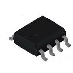
| 描述 | IC EARTH LEAKAGE DETECTOR 8-SOP模拟比较器 Earth Leak Detector |
| 产品分类 | |
| 品牌 | Fairchild Semiconductor |
| 产品手册 | |
| 产品图片 |
|
| rohs | 符合RoHS无铅 / 符合限制有害物质指令(RoHS)规范要求 |
| 产品系列 | 校验器 IC,Fairchild Semiconductor KA2803BDTF- |
| 数据手册 | |
| 产品型号 | KA2803BDTF |
| 产品种类 | 模拟比较器 |
| 供应商器件封装 | 8-SOP |
| 其它名称 | KA2803BDTFCT |
| 包装 | 剪切带 (CT) |
| 单位重量 | 143 mg |
| 响应时间 | 4 ms |
| 商标 | Fairchild Semiconductor |
| 安装类型 | 表面贴装 |
| 安装风格 | SMD/SMT |
| 封装 | Reel |
| 封装/外壳 | 8-SOIC(0.154",3.90mm 宽) |
| 封装/箱体 | SOP-8 |
| 工作温度 | -25°C ~ 80°C |
| 工厂包装数量 | 3000 |
| 应用 | 接地漏电检测器 |
| 最大工作温度 | + 85 C |
| 最小工作温度 | - 25 C |
| 标准包装 | 1 |
| 电压-电源 | 12 V ~ 20 V |
| 电流-电源 | 400µA |
| 电源电压-最大 | 18 V |
| 电源电压-最小 | 14 V |
| 电源电流 | 480 uA |
| 电源电流—最大值 | 480 uA |
| 系列 | KA2803B |
| 输出电流—典型值 | 800 uA |
| 零件号别名 | KA2803BDTF_NL |


PDF Datasheet 数据手册内容提取
Is Now Part of To learn more about ON Semiconductor, please visit our website at www.onsemi.com Please note: As part of the Fairchild Semiconductor integration, some of the Fairchild orderable part numbers will need to change in order to meet ON Semiconductor’s system requirements. Since the ON Semiconductor product management systems do not have the ability to manage part nomenclature that utilizes an underscore (_), the underscore (_) in the Fairchild part numbers will be changed to a dash (-). This document may contain device numbers with an underscore (_). Please check the ON Semiconductor website to verify the updated device numbers. The most current and up-to-date ordering information can be found at www.onsemi.com. Please email any questions regarding the system integration to Fairchild_questions@onsemi.com. ON Semiconductor and the ON Semiconductor logo are trademarks of Semiconductor Components Industries, LLC dba ON Semiconductor or its subsidiaries in the United States and/or other countries. ON Semiconductor owns the rights to a number of patents, trademarks, copyrights, trade secrets, and other intellectual property. A listing of ON Semiconductor’s product/patent coverage may be accessed at www.onsemi.com/site/pdf/Patent-Marking.pdf. ON Semiconductor reserves the right to make changes without further notice to any products herein. ON Semiconductor makes no warranty, representation or guarantee regarding the suitability of its products for any particular purpose, nor does ON Semiconductor assume any liability arising out of the application or use of any product or circuit, and specifically disclaims any and all liability, including without limitation special, consequential or incidental damages. Buyer is responsible for its products and applications using ON Semiconductor products, including compliance with all laws, regulations and safety requirements or standards, regardless of any support or applications information provided by ON Semiconductor. “Typical” parameters which may be provided in ON Semiconductor data sheets and/or specifications can and do vary in different applications and actual performance may vary over time. All operating parameters, including “Typicals” must be validated for each customer application by customer’s technical experts. ON Semiconductor does not convey any license under its patent rights nor the rights of others. ON Semiconductor products are not designed, intended, or authorized for use as a critical component in life support systems or any FDA Class 3 medical devices or medical devices with a same or similar classification in a foreign jurisdiction or any devices intended for implantation in the human body. Should Buyer purchase or use ON Semiconductor products for any such unintended or unauthorized application, Buyer shall indemnify and hold ON Semiconductor and its officers, employees, subsidiaries, affiliates, and distributors harmless against all claims, costs, damages, and expenses, and reasonable attorney fees arising out of, directly or indirectly, any claim of personal injury or death associated with such unintended or unauthorized use, even if such claim alleges that ON Semiconductor was negligent regarding the design or manufacture of the part. ON Semiconductor is an Equal Opportunity/Affirmative Action Employer. This literature is subject to all applicable copyright laws and is not for resale in any manner.
K A 2 8 0 January 2014 3 B — E a r t h KA2803B L e Earth Leakage Detector a k a g e D Features e Description t e Low Power Consumption: 5 mW, 100 V/200 V c The KA2803B is designed for use in earth leakage t o Built-In Voltage Regulator circuit interrupters, for operation directly off the AC line r in breakers. The input of the differential amplifier is High-Gain Differential Amplifier connected to the secondary coil of ZCT (Zero Current 0.4 mA Output Current Pulse to Trigger SCRs Transformer). The amplified output of differential amplifier is integrated at external capacitor to gain Low External Part Count adequate time delay specified in KSC4613. The level DIP & SOP Packages, High Packing Density comparator generates a high level when earth leakage current is greater than the fixed level. High Noise Immunity, Large Surge Margin Super Temperature Characteristic of Input Sensitivity Wide Operating Temperature Range: T = -25°C to +80°C A Operation from 12 V to 20 V Input 8-DIP Functions Differential Amplifier Level Comparator Latch Circuit 8-SOP Ordering Information Part Number Operating Temperature Range Package Packing Method KA2803B -25 to +80°C 8-Lead, Dual Inline Package (DIP) Tube © 2000 Fairchild Semiconductor Corporation www.fairchildsemi.com KA2803B • Rev. 1.0.8
K Block Diagram A 2 8 0 3 B — E a r t h L e a k a g e D e t e c to Figure 1. Block Diagram r Application Circuit Figure 2. Full-Wave Application Circuit Figure 3. Half-Wave Application Circuit Application Information (Refer to full-wave application circuit in Figure 2) used to protect the earth leakage detector IC (KA2803B). The range of R is from several hundred Figure 2 shows the KA2803B connected in a typical P Ω to several kΩ. leakage current detector system. The power is applied to the VCC terminal (Pin 8) directly from the power line. Capacitor C1 is for the noise canceller and a standard The resistor RS and capacitor CS are chosen so that Pin value of C1 is 0.047 µF. Capacitor C2 is also a noise 8 voltage is at least 12 V. The value of CS is canceller capacitance, but it is not usually used. recommended above 1 µF. When high noise is present, a 0.047 µF capacitor may If the leakage current is at the load, it is detected by the be connected between Pins 6 and 7. The amplified zero current transformer (ZCT). The output voltage signal finally appears at the Pin 7 with pulse signal signal of ZCT is amplified by the differential amplifier of through the internal latch circuit of the KA2803B. This the KA2803B internal circuit and appears as a half-cycle signal drives the gate of the external SCR, which sine wave signal referred to input signal at the output of energizes the trip coil, which opens the circuit breaker. the amplifier. The amplifier closed-loop gain is fixed The trip time of the breaker is determined by capacitor about 1000 times with internal feedback resistor to C and the mechanism breaker. This capacitor should 3 compensate for zero current transformer (ZCT) be selected under 1µF to satisfy the required trip time. variations. The resistor RL should be selected so that The full-wave bridge supplies power to the KA2803B the breaker satisfies the required sensing current. The during both the positive and negative half cycles of the protection resistor RP is not usually used when high line voltage. This allows the hot and neutral lines to be current is injected at the breaker; this resistor should be interchanged. © 2000 Fairchild Semiconductor Corporation www.fairchildsemi.com KA2803B • Rev. 1.0.8 2
K Absolute Maximum Ratings A 2 Stresses exceeding the absolute maximum ratings may damage the device. The device may not function or be 8 0 operable above the recommended operating conditions and stressing the parts to these levels is not recommended. 3 In addition, extended exposure to stresses above the recommended operating conditions may affect device reliability. B The absolute maximum ratings are stress ratings only. — E Symbol Parameter Min. Max. Unit a r t VCC Supply Voltage 20 V h L I Supply Current 8 mA CC e a PD Power Dissipation 300 mW k a TL Lead Temperature, Soldering 10 Seconds 260 °C g e T Operation Temperature Range -25 +80 °C A D e T Storage Temperature Range -65 +150 °C STG t e c t o r Electrical Characteristics T = -25°C to +80°C unless otherwise specified. A Test Symbol Parameter Conditions Min. Typ. Max. Units Circuit T = -25°C 580 V =12V A CC I Supply Current 1 V =OPEN T = +25°C Figure 4 300 400 530 µA CC R A V=2 V I T = +80°C 480 A V =16 V, VT Trip Voltage VCRC=2 V~2.02 V, VI=2 Figure 5 14 16 18 (mmVs) Note 1 12.5 14.2 17.0 Differential Amplifier Current V =16 V, V ~V=30 mV, CC R I Figure 7 -12 20 -30 Current 1 V =1.2 V OD I µA O(D) Differential Amplifier Current V =16 V, V =0.8 V,V , CC OD R Figure 8 17 27 37 Current 2 V Short=V I P T = -25°C 200 400 800 V =1.4 V, A SC I Output Current V =0.8 V, T = +25°C Figure 9 200 400 800 µA O OS A V =16.0 V CC T = +80°C 100 300 600 A V Latch-On Voltage V =16 V Figure 10 0.7 1.0 1.4 V SCON CC I Latch Input Current V =16 V Figure 11 -13 -7 -1 µA SCON CC I Output Low Current V =12 V, V =0.2 V Figure 12 200 800 1400 µA OSL CC OSL V Differential Input Clamp Voltage V =16 V, I =100 mA Figure 13 0.4 1.2 2.0 V IDC CC IDC V Maximum Current Voltage I =7 mA Figure 14 20 24 28 V SM SM I Supply Current 2 V =12.0 V, V =0.6 V Figure 15 200 400 900 µA S2 CC OSL V =12.0 V OS V Latch-Off Supply Voltage V =1.8 V Figure 16 7 8 9 V SOFF SC I =100.0 mA IDC V =16 V, V -V=0.3 V, t Response Time CC R I Figure 17 2 3 4 ms ON 1 V<V <5 V X Note: 1. Guaranteed by design, not tested in production. © 2000 Fairchild Semiconductor Corporation www.fairchildsemi.com KA2803B • Rev. 1.0.8 3
Test Circuits Figure 4. Supply Current 1 Figure 5. Trip Voltage Figure 6. V for V Measurement Figure 7. Differential Amplifier Output Current 1 PN1 P Figure 8. Differential Amplifier Output Current 2 Figure 9. Output Current © 2000 Fairchild Semiconductor Corporation www.fairchildsemi.com KA2803B • Rev. 1.0.8 4
Test Circuits (Continued) Figure 10. Latch-On Voltage Figure 11. Latch Input Current Figure 12. Output Low Current Figure 13. Differential Input Clamp Voltage Figure 14. Maximum Current Voltage Figure 15. Supply Current 2 Figure 16. Latch-Off Supply Voltage Figure 17. Response Time © 2000 Fairchild Semiconductor Corporation www.fairchildsemi.com KA2803B • Rev. 1.0.8 5
Typical Performance Characteristics Figure 18. Supply Current Figure 19. Differential Amplifier Output Current (V -V=30 mV, V =1.2 V) R I OD Figure 20. Differential Amplifier Output Current Figure 21.Output Current (V , V=V , V =0.8 V) R I P OD Figure 22. Output Low Current Figure 23.V Voltage vs. Supply Current1 CC © 2000 Fairchild Semiconductor Corporation www.fairchildsemi.com KA2803B • Rev. 1.0.8 6
K A Typical Performance Characteristics (Continued) 2 8 0 3 B — E a r t h L e a k a g e D e t e c t o r Figure 24. Differential Amplifier Output Current 1 Figure 25.Differential Amplifier Output Figure 26. Latch Input Current Figure 27.Output Low Current Figure 28. Output Current Figure 29.V Voltagevs. Supply Current 2 CC © 2000 Fairchild Semiconductor Corporation www.fairchildsemi.com KA2803B • Rev. 1.0.8 7
K Typical Performance Characteristics (Continued) A 2 8 0 3 B — E a r t h L e a k a g e D e t e c t o Figure 30. Differential Input Clamp Voltage Figure 31.Latch-Off Supply Voltage r Figure 32. Latch-On Input Voltage Figure 33.Maximum Supply Figure 34. Trip and Output Figure 35.Output Response Time © 2000 Fairchild Semiconductor Corporation www.fairchildsemi.com KA2803B • Rev. 1.0.8 8
K Physical Dimensions A 2 8 0 3 .400[10.15] B A .373 9.46 — .036 [0.9 TYP] E a r (.092) [Ø2.337] t h PIN #1 (.032) [R0.813] L e .250±.005 [6.35±0.13] a PIN #1 k a g e B D TOP VIEW TOP VIEW e t OPTION 1 OPTION 2 e c t .070[1.78] o .045 1.14 .310±.010 [7.87±0.25] r .130±.005 [3.3±0.13] 7° TYP .210 MAX [5.33] 7° TYP C .015 MIN .021[0.53] [0.38] .015 0.37 .140[3.55] .300 .125 3.17 [7.62] .001[.025] C .100 .430 MAX [2.54] [10.92] NOTES: .060 MAX [1.52] A. CONFORMS TO JEDEC REGISTRATION MS-001, +.005[ +0.127] VARIATIONS BA .010-.000 0.254-0.000 B. CONTROLING DIMENSIONS ARE IN INCHES REFERENCE DIMENSIONS ARE IN MILLIMETERS C. DOES NOT INCLUDE MOLD FLASH OR PROTRUSIONS. MOLD FLASH OR PROTRUSIONS SHALL NOT EXCEED .010 INCHES OR 0.25MM. D. DOES NOT INCLUDE DAMBAR PROTRUSIONS. DAMBAR PROTRUSIONS SHALL NOT EXCEED .010 INCHES OR 0.25MM. E. DIMENSIONING AND TOLERANCING PER ASME Y14.5M-1994. N08EREVG Figure 36. 8-Lead, Dual Inline Package (DIP) Package drawings are provided as a service to customers considering Fairchild components. Drawings may change in any manner without notice. Please note the revision and/or date on the drawing and contact a Fairchild Semiconductor representative to verify or obtain the most recent revision. Package specifications do not expand the terms of Fairchild’s worldwide terms and conditions, specifically the warranty therein, which covers Fairchild products. Always visit Fairchild Semiconductor’s online packaging area for the most recent package drawings: http://www.fairchildsemi.com/packaging/. © 2000 Fairchild Semiconductor Corporation www.fairchildsemi.com KA2803B • Rev. 1.0.8 9
K A Physical Dimensions 2 8 0 3 B — 0.65 E 4.90±0.10 A a (0.635) r t 8 5 h B L e a k 1.75 a 6.00±0.20 g 3.90±0.10 5.60 e D e t e c t o 1 4 r PIN ONE INDICATOR 1.27 1.27 0.25 C B A LAND PATTERN RECOMMENDATION SEE DETAIL A 0.175±0.75 0.22±0.30 1.75 MAX C 0.10 0.42±0.09 OPTION A - BEVEL EDGE (0.86) x 45° R0.10 GAGE PLANE R0.10 OPTION B - NO BEVEL EDGE 0.36 8° NOTES: UNLESS OTHERWISE SPECIFIED 0° A) THIS PACKAGE CONFORMS TO JEDEC MS-012, VARIATION AA. SEATING PLANE B) ALL DIMENSIONS ARE IN MILLIMETERS. 0.65±0.25 C) DIMENSIONS DO NOT INCLUDE MOLD FLASH OR BURRS. (1.04) D) LANDPATTERN STANDARD: SOIC127P600X175-8M. DETAIL A E) DRAWING FILENAME: M08Arev15 SCALE: 2:1 F) FAIRCHILD SEMICONDUCTOR. Figure 37. 8-Lead, Small Outline Package (SOP) Package drawings are provided as a service to customers considering Fairchild components. Drawings may change in any manner without notice. Please note the revision and/or date on the drawing and contact a Fairchild Semiconductor representative to verify or obtain the most recent revision. Package specifications do not expand the terms of Fairchild’s worldwide terms and conditions, specifically the warranty therein, which covers Fairchild products. Always visit Fairchild Semiconductor’s online packaging area for the most recent package drawings: http://www.fairchildsemi.com/packaging/. © 2000 Fairchild Semiconductor Corporation www.fairchildsemi.com KA2803B • Rev. 1.0.8 10
K A 2 8 0 3 B — E a r t h L e a k a g e D e t e c t o r © 2000 Fairchild Semiconductor Corporation www.fairchildsemi.com KA2803B • Rev. 1.0.8 11
ON Semiconductor and are trademarks of Semiconductor Components Industries, LLC dba ON Semiconductor or its subsidiaries in the United States and/or other countries. ON Semiconductor owns the rights to a number of patents, trademarks, copyrights, trade secrets, and other intellectual property. A listing of ON Semiconductor’s product/patent coverage may be accessed at www.onsemi.com/site/pdf/Patent−Marking.pdf. ON Semiconductor reserves the right to make changes without further notice to any products herein. ON Semiconductor makes no warranty, representation or guarantee regarding the suitability of its products for any particular purpose, nor does ON Semiconductor assume any liability arising out of the application or use of any product or circuit, and specifically disclaims any and all liability, including without limitation special, consequential or incidental damages. Buyer is responsible for its products and applications using ON Semiconductor products, including compliance with all laws, regulations and safety requirements or standards, regardless of any support or applications information provided by ON Semiconductor. “Typical” parameters which may be provided in ON Semiconductor data sheets and/or specifications can and do vary in different applications and actual performance may vary over time. All operating parameters, including “Typicals” must be validated for each customer application by customer’s technical experts. ON Semiconductor does not convey any license under its patent rights nor the rights of others. ON Semiconductor products are not designed, intended, or authorized for use as a critical component in life support systems or any FDA Class 3 medical devices or medical devices with a same or similar classification in a foreign jurisdiction or any devices intended for implantation in the human body. Should Buyer purchase or use ON Semiconductor products for any such unintended or unauthorized application, Buyer shall indemnify and hold ON Semiconductor and its officers, employees, subsidiaries, affiliates, and distributors harmless against all claims, costs, damages, and expenses, and reasonable attorney fees arising out of, directly or indirectly, any claim of personal injury or death associated with such unintended or unauthorized use, even if such claim alleges that ON Semiconductor was negligent regarding the design or manufacture of the part. ON Semiconductor is an Equal Opportunity/Affirmative Action Employer. This literature is subject to all applicable copyright laws and is not for resale in any manner. PUBLICATION ORDERING INFORMATION LITERATURE FULFILLMENT: N. American Technical Support: 800−282−9855 Toll Free ON Semiconductor Website: www.onsemi.com Literature Distribution Center for ON Semiconductor USA/Canada 19521 E. 32nd Pkwy, Aurora, Colorado 80011 USA Europe, Middle East and Africa Technical Support: Order Literature: http://www.onsemi.com/orderlit Phone: 303−675−2175 or 800−344−3860 Toll Free USA/Canada Phone: 421 33 790 2910 Fax: 303−675−2176 or 800−344−3867 Toll Free USA/Canada Japan Customer Focus Center For additional information, please contact your local Email: orderlit@onsemi.com Phone: 81−3−5817−1050 Sales Representative © Semiconductor Components Industries, LLC www.onsemi.com www.onsemi.com 1
Mouser Electronics Authorized Distributor Click to View Pricing, Inventory, Delivery & Lifecycle Information: O N Semiconductor: KA2803B KA2803BDTF