ICGOO在线商城 > 集成电路(IC) > PMIC - 电源控制器,监视器 > LTC2950CDDB-1#TRMPBF

 Datasheet下载
- 型号: LTC2950CDDB-1#TRMPBF
- 制造商: LINEAR TECHNOLOGY
- 库位|库存: xxxx|xxxx
- 要求:
| 数量阶梯 | 香港交货 | 国内含税 |
| +xxxx | $xxxx | ¥xxxx |
查看当月历史价格
查看今年历史价格
LTC2950CDDB-1#TRMPBF产品简介:
ICGOO电子元器件商城为您提供LTC2950CDDB-1#TRMPBF由LINEAR TECHNOLOGY设计生产,在icgoo商城现货销售,并且可以通过原厂、代理商等渠道进行代购。 LTC2950CDDB-1#TRMPBF价格参考。LINEAR TECHNOLOGYLTC2950CDDB-1#TRMPBF封装/规格:PMIC - 电源控制器,监视器, Power Supply Controller Push Button, On/Off Controller 8-DFN (3x2)。您可以下载LTC2950CDDB-1#TRMPBF参考资料、Datasheet数据手册功能说明书,资料中有LTC2950CDDB-1#TRMPBF 详细功能的应用电路图电压和使用方法及教程。
LTC2950CDDB-1#TRMPBF 是 Linear Technology(现为 Analog Devices)生产的一款 PMIC(电源管理集成电路),属于电源控制器和监视器类别。这款芯片主要应用于需要精确电压、电流监测以及多路电源管理的场景,以下是其典型应用场景:

 1. 工业控制系统
   - 在工业自动化设备中,LTC2950 可用于监控和控制多个供电轨的状态,确保系统运行在安全范围内。
   - 应用于 PLC(可编程逻辑控制器)、DCS(分布式控制系统)等,提供高精度的电源状态反馈。

 2. 通信设备
   - 在基站、路由器和其他通信设备中,LTC2950 可以实时监测电源电压和电流,防止因电源异常导致设备故障。
   - 支持对多路电源的独立监控,适用于复杂的通信系统架构。

 3. 数据中心与服务器
   - 数据中心的电源管理系统需要高可靠性和精确性,LTC2950 可用于监控服务器主板上的多个供电轨。
   - 提供过压、欠压保护功能,确保关键组件的安全运行。

 4. 医疗设备
   - 在医疗设备中(如监护仪、超声设备等),LTC2950 能够精确监测电源状态,保障设备稳定性和患者安全。
   - 实现低功耗设计,适合便携式医疗设备。

 5. 汽车电子
   - 用于车载信息娱乐系统、ADAS(高级驾驶辅助系统)等,监控电池电压和电流,防止过充或过放。
   - 提供快速响应的电源故障检测,增强系统的安全性。

 6. 消费类电子产品
   - 在高端消费电子产品(如笔记本电脑、平板电脑)中,LTC2950 可用于优化电源管理,延长电池寿命。
   - 提供高效的电源切换和负载管理功能。

 核心优势:
- 多路电源监控:支持同时监测多个电源轨。
- 高精度测量:提供准确的电压、电流和功率数据。
- 灵活配置:可通过 I2C 接口进行参数设置和状态读取。
- 保护功能:内置过压、欠压、过流保护,提高系统可靠性。

总之,LTC2950CDDB-1#TRMPBF 适用于需要高性能电源管理和监控的复杂系统,广泛应用于工业、通信、医疗、汽车和消费电子等领域。
| 参数 | 数值 |
| 产品目录 | 集成电路 (IC) |
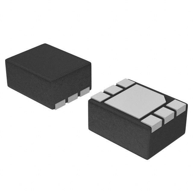
| 描述 | IC PUSH BUTTON ON/OFF CTRLR 8DFN |
| 产品分类 | |
| 品牌 | Linear Technology |
| 数据手册 | http://www.linear.com/docs/7377 |
| 产品图片 |
|
| 产品型号 | LTC2950CDDB-1#TRMPBF |
| rohs | 无铅 / 符合限制有害物质指令(RoHS)规范要求 |
| 产品系列 | - |
| 产品培训模块 | http://www.digikey.cn/PTM/IndividualPTM.page?site=cn&lang=zhs&ptm=13048 |
| 产品目录页面 | |
| 供应商器件封装 | 8-DFN(3x2) |
| 其它名称 | LTC2950CDDB-1#TRMPBFDKR |
| 包装 | Digi-Reel® |
| 安装类型 | 表面贴装 |
| 封装/外壳 | 8-WFDFN 裸露焊盘 |
| 工作温度 | 0°C ~ 70°C |
| 应用 | 按钮,开/关控制器 |
| 标准包装 | 1 |
| 电压-电源 | 2.7 V ~ 26.4 V |
| 电压-输入 | - |
| 电流-电源 | 6µA |
| 配用 | /product-detail/zh/DC826B-A/DC826B-A-ND/3028639 |


- 商务部:美国ITC正式对集成电路等产品启动337调查
- 曝三星4nm工艺存在良率问题 高通将骁龙8 Gen1或转产台积电
- 太阳诱电将投资9.5亿元在常州建新厂生产MLCC 预计2023年完工
- 英特尔发布欧洲新工厂建设计划 深化IDM 2.0 战略
- 台积电先进制程称霸业界 有大客户加持明年业绩稳了
- 达到5530亿美元!SIA预计今年全球半导体销售额将创下新高
- 英特尔拟将自动驾驶子公司Mobileye上市 估值或超500亿美元
- 三星加码芯片和SET,合并消费电子和移动部门,撤换高东真等 CEO
- 三星电子宣布重大人事变动 还合并消费电子和移动部门
- 海关总署:前11个月进口集成电路产品价值2.52万亿元 增长14.8%


PDF Datasheet 数据手册内容提取
LTC2950-1/LTC2950-2 Pushbutton On/Off Controller FeaTures DescripTion n Adjustable Pushbutton On/Off Timers The LTC®2950 is a micropower, wide input voltage range, n Low Supply Current: 6µA pushbutton ON/OFF controller. The part contains a pushbut- n Wide Operating Voltage Range: 2.7V to 26.4V ton input with independently programmable ON and OFF n EN Output (LTC2950-1) Allows DC/DC Converter debounce times that control the toggling of an open drain Control enable output. The part also contains a simple micropro- n EN Output (LTC2950-2) Allows Circuit Breaker cessor interface to allow for proper system housekeeping Control prior to power down. Under system fault conditions, an n Simple Interface Allows Graceful µP Shut Down internal KILL timer ensures proper power down. n High Input Voltage PB Pin with Internal Pull Up The LTC2950 operates over a wide 2.7V to 26.4V input Resistor voltage range to accommodate a wide variety of input n ±10kV ESD HBM on PB Input power supplies. Very low quiescent current (6µA typical) n Accurate 0.6V Threshold on KILL Comparator Input makes the LTC2950 ideally suited for battery powered n 8-Pin 3mm × 2mm DFN and ThinSOT™ Packages applications. Two versions of the part are available to ac- commodate either positive or negative enable polarities. applicaTions The parts are available in either 8-lead 3mm × 2mm DFN or ThinSOT packages. n Portable Instrumentation Meters n Blade Servers L, LT, LTC, LTM, Linear Technology and the Linear logo are registered trademarks and ThinSOT and PowerPath are trademarks of Linear Technology Corporation. All other trademarks n Portable Customer Service PDA are the property of their respective owners. n Desktop and Notebook Computers Typical applicaTion Turn On Debounce VIN 2.7V TO 26.4V VIN VOUT DC/DC BUCK SHDN** EN R1 2V/DIV VIN EN 10k LTC2950-1 INT INT PB µP/µC PB KILL KILL GND ONT OFFT 2950 TA01 10ms/DIV 2950 TA01b CONT* COFFT* 0.033µF 0.033µF *OPTIONAL **SHDN INTERNALLY PULLED UP BY DC/DC 295012fd 1
LTC2950-1/LTC2950-2 absoluTe MaxiMuM raTings (Note 1) Supply Voltage (V ) ..................................–0.3V to 33V Operating Temperature Range IN Input Voltages LTC2950C-1 .............................................0°C to 70°C PB .............................................................–6V to 33V LTC2950C-2 .............................................0°C to 70°C ONT ......................................................–0.3V to 2.7V LTC2950I-1 ..........................................–40°C to 85°C OFFT .....................................................–0.3V to 2.7V LTC2950I-2 ..........................................–40°C to 85°C KILL .........................................................–0.3V to 7V Storage Temperature Range Output Voltages DFN Package .....................................–65°C to 125°C INT .........................................................–0.3V to 10V TSOT-23 .............................................–65°C to 150°C EN/EN ....................................................–0.3V to 10V Lead Temperature (Soldering, 10 sec) ...................300°C pin conFiguraTion TOP VIEW TOP VIEW GND 1 8 INT ONT 2 7 EN/EN VIN 1 8 KILL 9 PB 2 7 OFFT PB 3 6 OFFT ONT 3 6 EN/EN VIN 4 5 KILL GND 4 5 INT TS8 PACKAGE DDB8 PACKAGE 8-LEAD PLASTIC TSOT-23 8-LEAD (3mm × 2mm) PLASTIC DFN TJMAX = 125°C, θJA = 140°C/W TJMAX = 125°C, θJA = 165°C/W EXPOSED PAD (PIN 9) PCB GND CONNECTION OPTIONAL orDer inForMaTion Lead Free Finish TAPE AND REEL (MINI) TAPE AND REEL PART MARKING* PACKAGE DESCRIPTION TEMPERATURE RANGE LTC2950CDDB-1#TRMPBF LTC2950CDDB-1#TRPBF LBKP 8-Lead Plastic DFN 0°C to 70°C LTC2950CDDB-2#TRMPBF LTC2950CDDB-2#TRPBF LBNG 8-Lead Plastic DFN 0°C to 70°C LTC2950IDDB-1#TRMPBF LTC2950IDDB-1#TRPBF LBKP 8-Lead Plastic DFN –40°C to 85°C LTC2950IDDB-2#TRMPBF LTC2950IDDB-2#TRPBF LBNG 8-Lead Plastic DFN –40°C to 85°C LTC2950CTS8-1#TRMPBF LTC2950CTS8-1#TRPBF LTBKN 8-Lead Plastic TSOT-23 0°C to 70°C LTC2950CTS8-2#TRMPBF LTC2950CTS8-2#TRPBF LTBNF 8-Lead Plastic TSOT-23 0°C to 70°C LTC2950ITS8-1#TRMPBF LTC2950ITS8-1#TRPBF LTBKN 8-Lead Plastic TSOT-23 –40°C to 85°C LTC2950ITS8-2#TRMPBF LTC2950ITS8-2#TRPBF LTBNF 8-Lead Plastic TSOT-23 –40°C to 85°C TRM = 500 pieces. *Temperature grades are identified by a label on the shipping container. Consult LTC Marketing for parts specified with wider operating temperature ranges. Consult LTC Marketing for information on lead based finish parts. For more information on lead free part marking, go to: http://www.linear.com/leadfree/ For more information on tape and reel specifications, go to: http://www.linear.com/tapeandreel/ 295012fd 2
LTC2950-1/LTC2950-2 elecTrical characTerisTics The l denotes the specifications which apply over the full operating temperature range, otherwise specifications are at T = 25°C. V = 2.7V to 26.4V, unless otherwise noted. (Note 2) A IN SYMBOL PARAMETER CONDITIONS MIN TYP MAX UNITS V Supply Voltage Range Steady State Operation l 2.7 26.4 V IN I V Supply Current System Power On, V = 2.7V to 24V l 6 12 µA IN IN IN V V Undervoltage Lockout V Falling l 2.2 2.3 2.4 V UVL IN IN V V Undervoltage Lockout 50 300 600 mV UVL(HYST) IN Hysteresis Pushbutton, Enable (PB, EN/EN) V PB Voltage Range Single-Ended l –1 26.4 V PB(MIN, MAX) I PB Input Current 2.5V < V < 26.4V l ±1 µA PB PB V = 1V l –1 –6 –12 µA PB V = 0.6V l –3 –9 –15 µA PB V PB Input Threshold PB Falling l 0.6 0.8 1 V PB(VTH) V PB Open Circuit Voltage I = –1µA 1 1.6 2 V PB(VOC) PB tEN/EN, Lock Out EN/EN Lock Out Time (Note 5) Enable Released → Enable Asserted l 200 256 325 ms I EN/EN Leakage Current V = 1V, Sink Current Off l ±0.1 µA EN/EN(LKG) EN/EN V EN/EN Voltage Output Low I = 3mA l 0.11 0.4 V EN/EN(VOL) EN/EN Debounce Timing Pins (ONT, OFFT) I ONT/OFFT Pull Up Current V = 0V l –2.4 –3 –3.6 µA ONT, OFFT(PU) ONT, OFFT I ONT/OFFT Pull Down Current V = 1.3V l 2.4 3 3.6 µA ONT, OFFT(PD) ONT, OFFT tDB, On Internal Turn On Debounce Time ONT Pin Float, PB Falling → Enable Asserted l 26 32 41 ms t Additional Adjustable Turn On Time C = 1500pF l 9 11.5 13.5 ms ONT ONT tDB, Off Internal Turn Off Debounce Time OFFT Pin Float, PB Falling → INT Falling l 26 32 41 ms t Additional Adjustable Turn Off Time C = 1500pF l 9 11.5 13.5 ms OFFT OFFT µP Handshake Pins (INT, KILL) I INT Leakage Current V = 3V l ±1 µA INT(LKG) INT V INT Output Voltage Low I = 3mA l 0.11 0.4 V INT(VOL) INT V KILL Input Threshold Voltage KILL Falling l 0.57 0.6 0.63 V KILL(TH) V KILL Input Threshold Hysteresis 10 30 50 mV KILL(HYST) I KILL Leakage Current V = 0.6V ±0.1 µA KILL(LKG) KILL t KILL Minimum Pulse Width l 30 µs KILL(PW) tKILL(PD) KILL Propagation Delay KILL Falling → Enable Released l 30 µs tKILL, On Blank KILL Turn On Blanking (Note 3) KILL = Low, Enable Asserted → Enable Released l 400 512 650 ms tKILL, Off Delay KILL Turn Off Delay (Note 4) KILL = High, INT Asserted → Enable Released l 800 1024 1300 ms Note 1: Stresses beyond those listed under Absolute Maximum Ratings Note 4: The KILL turn off delay is the maximum delay from the initiation may cause permanent damage to the device. Exposure to any Absolute of a shutdown sequence (INT falling), to the release of the enable output. Maximum Rating condition for extended periods may affect device If the KILL input switches low at any time during this period, enable is reliability and lifetime. released, thus turning off system power. This time is internally fixed at Note 2: All currents into pins are positive; all voltages are referenced to 1024ms. This time delay does not include tDB, OFF or tOFFT. GND unless otherwise noted. Note 5: The enable lock out time is designed to allow an application to Note 3: The KILL turn on blanking timer period is the waiting period properly power down such that the next power up sequence starts from a immediately after the enable output is asserted. This blanking time allows consistent powered down configuration. PB is ignored during this lock out sufficient time for the DC/DC converter and the µP to perform power up time. This time delay does not include tDB, ON or tONT. tasks. The KILL and PB inputs are ignored during this period. If KILL remains low at the end of this time period, the enable output is released, thus turning off system power. This time delay does not include t or t . DB, ON ONT 295012fd 3
LTC2950-1/LTC2950-2 Typical perForMance characTerisTics Internal Default Turn On Supply Current vs Temperature Supply Current vs Supply Voltage Debounce Time (tDB, ON) vs VIN 10 10 50 VIN = 26.4V TA = 25°C TA = 25°C 8 8 40 A) 6 VIN = 3.3V A) 6 ms) 30 (µN VIN = 2.7V (µN (ON IVI 4 IVI 4 DB, 20 t 2 2 10 0 0 0 –50 –25 0 25 50 75 100 0 5 10 15 20 25 30 0 5 10 15 20 25 30 TEMPERATURE (°C) VIN (V) VIN (V) 2950 G01 2950 G02 2950 G03 Turn On Debounce Time (tDB, ON ONT Pull-Down Current Internal Default Turn Off + tONT) vs ONT External Capacitor vs Temperature Debounce Time (tDB, OFF) vs VIN 10000 –3.4 50 TA = 25°C TA = 25°C VIN = 3.3V µA) 40 T ( –3.2 s) 1000 EN m R + t (DB, ONONT 100 LL-DOWN CUR –3.0 VIN = 2.7VVIN = 26.4V t (ms)DB, OFF 3200 t U NT P –2.8 10 O 10 –2.6 0 1 10 100 1000 –50 –25 0 25 50 75 100 0 5 10 15 20 25 30 ONT EXTERNAL CAPACITOR (nF) TEMPERATURE (°C) VIN (V) 2950 G04 2950 G05 2950 G06 Turn Off Debounce Time (tDB, OFF OFFT Pull-Down Current + tOFFT) vs OFFT External Capacitor vs Temperature PB Current vs PB Voltage 10000 –3.4 –250 TA = 25°C TA = 25°C VIN = 3.3V VIN = 3.3V A) µ –200 T ( –3.2 ms) 1000 REN A) t + t (DB, OFFOFFT 100 T PULL-DOWN CUR ––32..08 VIN = 2.7VVIN = 26.4V PB CURRENT (µ––115000 FF –50 O 10 –2.6 0 1 10 100 1000 –50 –25 0 25 50 75 100 –10 –5 0 5 10 15 20 25 30 OFFT EXTERNAL CAPACITOR (nF) TEMPERATURE (°C) PB VOLTAGE (V) 2950 G07 2950 G08 2950 G09 295012fd 4
LTC2950-1/LTC2950-2 Typical perForMance characTerisTics PB Voltage vs External PB Resistance to Ground EN/EN V vs Current Load OL 300 500 VIN = 3.3V TA = 25°C VIN = 3.3V 250 400 V)200 mV) E (m TA = 100°C GE ( 300 G A LTA150 TA = 25°C OLT PB VO100 TA = –45°C N/EN V 200 E 100 50 0 0 0 5 10 15 20 0 2 4 6 8 10 EXTERNAL PB RESISTANCE TO GROUND (kΩ) EN/EN CURRENT LOAD (mA) 2950 G10 2950 G11 EN (LTC2950-1) Voltage vs VIN EN (LTC2950-2) Voltage vs VIN 1.0 4 TA = 25°C TA = 25°C 100k PULL-UP FROM EN TO VIN 100k PULL-UP FROM EN TO VIN 0.8 3 0.6 V) V) N ( N ( 2 E E 0.4 1 0.2 0 0 0 1 2 3 4 0 1 2 3 4 VIN (V) VIN (V) 2950 G12 2950 G13 295012fd 5
LTC2950-1/LTC2950-2 pin FuncTions (TSOT-23/DFN) V (Pin 1/Pin 4): Power Supply Input: 2.7V to 26.4V. turn-off) is detected. This pin can connect directly to a IN DC/DC converter shutdown pin that provides an internal PB (Pin 2/Pin 3): Pushbutton Input. Connecting PB to pull-up. Otherwise a pull-up resistor to an external supply ground through a momentary switch provides on/off is required. The operating range for this pin is 0V to 10V. control via the EN/EN pin. An internal 100k pull-up resis- tor connects to an internal 1.9V bias voltage. The rugged EN (LTC2950-2, Pin 6/Pin 7): Open Drain Enable Output. PB input can be pulled up to 26.4V externally without This pin is intended to enable system power. EN is asserted consuming extra current. low after a valid PB turn-on event. EN releases high if: a) KILL is not driven high (by µP) within 512ms of the initial ONT (Pin 3/Pin 2): Additional Adjustable Turn On Time valid PB power turn-on event, b) KILL is driven low dur- Input. Placing an external capacitor to ground determines ing normal operation, c) a second valid PB event (power the additional time (beyond the internal default 32ms) turn-off) is detected. This pin can connect directly to a the PB pin must be held low before the enable output DC/DC converter shutdown pin that provides an internal is asserted. Floating this pin results in a default turn on pull-up. Otherwise a pull-up resistor to an external supply debounce time of 32ms. is required. The operating range of this pin is 0V to 10V. GND (Pin 4/Pin 1): Device Ground. OFFT (Pin 7/Pin 6): Additional Adjustable Turn Off Time INT (Pin 5/Pin 8): Open Drain Interrupt Output. After a Input. A capacitor to ground determines the additional pushbutton turn-off event is detected, the LTC2950 inter- time (beyond the internal default 32ms) that the PB pin rupts the system (µP) by bringing the INT pin low. Once the must be held low before initiating a power down sequence system finishes its power down and housekeeping tasks, (INT falling). Floating this pin results in a default turn off it sets KILL low, which in turn releases the enable output. time of 32ms. If at the end of the power down timer (1024ms) KILL is KILL (Pin 8/Pin 5): KILL Input. Forcing KILL low releases still high, the enable output is released immediately. INT the enable output. During system turn on, this pin is blanked may optionally be tied to KILL to release the enable output by a 512ms internal timer to allow the system to pull KILL immediately after the turn-off event has been detected high. This pin has an accurate 0.6V threshold and can be (INT = low). used as a voltage monitor input. If unused, connect to a EN (LTC2950-1, Pin 6/Pin 7): Open Drain Enable Output. low voltage output supply (see Figure 6). This pin is intended to enable system power. EN is asserted Exposed Pad (Pin 9): Exposed Pad may be left open or high after a valid PB turn on event. EN is released low if: a) connected to device ground. KILL is not driven high (by µP) within 512ms of the initial valid PB power turn-on event, b) KILL is driven low dur- ing normal operation, c) a second valid PB event (power 295012fd 6
LTC2950-1/LTC2950-2 block DiagraM EN/EN VIN 2.7V TO 26.4V REGULATOR 2.4V 2.4V KILL OSCILLATOR 100k PB LOGIC 10µS FILTER DEBOUNCE 0.6V 0.8V INT OSCILLATOR GND ONT OFFT 2950 BD TiMing DiagraMs tKILL(PW) KILL tKILL(PD) EN/EN 2950 TD01 295012fd 7
LTC2950-1/LTC2950-2 TiMing DiagraMs PB PB & KILL IGNORED tDB, ON tONT tKILL, ON BLANK 16 CYCLES EN (LTC2950-1) EN (LTC2950-2) 2950 TD02 Power On Timing PB PB IGNORED tDB, OFF tOFFT OFFT 16 CYCLES INT tKILL, OFF DELAY EN (LTC2950-1) EN (LTC2950-2) 2950 TD03 Power Off Timing, KILL > 0.6V 295012fd 8
LTC2950-1/LTC2950-2 applicaTions inForMaTion Description Note that the KILL input can be pulled low (thereby releasing the enable output) at any time after t , ON BLANK period. The LTC2950 is a low power (6µA), wide input voltage KILL range (2.7V to 26.4V), pushbutton on/off controller that Simplified Power On/Off Sequence can interface to a µP and a power supply. The turn-on and turn-off debounce times are extendable using optional Figure 1 shows a simplified LTC2950-1 power on and power external capacitors. A simple interface (INT output, KILL off sequence. A high to low transition on PB (t ) initiates 1 input) allows a system to power on and power off in a the power on sequence. This diagram does not show any controlled manner. bounce on PB. In order to assert the enable output, the PB pin must stay low continuously (PB high resets timers) Turn On for a time controlled by the default 32ms and the external ONT capacitor (t –t ). Once EN goes high (t ), an internal When power is first applied to the LTC2950, the part ini- 2 1 2 512ms blanking timer is started. This blanking timer is tializes the output pins. Any DC/DC converters connected designed to give sufficient time for the DC/DC converter to the EN/EN pin will therefore be held off. To assert the to reach its final voltage, and to allow the µP enough time enable output, PB must be held low for a minimum of to perform power on tasks. 32ms (t ). The LTC2950 provides additional turn on DB, ON debounce time via an optional capacitor connected to the The KILL pin must be pulled high within 512ms of the EN ONT pin (t ). The following equation describes the ad- pin going high. Failure to do so results in the EN pin going ONT ditional time that PB must be held low before asserting low 512ms after it went high. (EN = low, see Figure 2). the enable output. C is the ONT external capacitor: Note that the LTC2950 does not sample KILL and PB until ONT after the 512ms internal timer has expired. The reason PB C = 1.56E-4 [µF/ms] • (t – 1ms) ONT ONT is ignored is to ensure that the system is not forced off Once the enable output is asserted, any DC/DC converters while powering on. Once the 512ms timer expires (t ), the 4 connected to this pin are turned on. The KILL input from release of the PB pin is then debounced with an internal the µP is ignored during a succeeding 512ms blanking 32ms timer. The system has now properly powered on time (tKILL, ON BLANK). This blanking time represents the and the LTC2950 monitors PB and KILL (for a turnoff maximum time required to power up the DC/DC converter command) while consuming only 6µA of supply current. and the µP. If KILL is not brought high during this 512ms A high to low transition on PB (t ) initiates the power off time window, the enable output is released. The assumption 5 sequence. PB must stay low continuously (PB high resets is that 512ms is sufficient time for the system to power up. debounce timer) for a period controlled by the default 32ms and the external OFFT capacitor (t –t ). At the completion Turn Off 6 5 of the OFFT timing (t ), an interrupt (INT) is set, signifying 6 To initiate a power off sequence, PB must be held low for a that EN will be switched low in 1024ms. Once a system minimum of 32ms (t ). Additional turn off debounce DB, OFF has finished performing its power down operations, it time may be added via an optional capacitor connected can set KILL low (t ) and thus immediately set EN low), 7 to the OFFT pin (t ). The following equation describes OFFT terminating the internal 1024ms timer. The release of the the additional time that PB must be held low to initiate a PB pin is then debounced with an internal 32ms timer. power off sequence. C is the OFFT external capacitor: OFFT The system is now in its reset state: where the LTC2950 C = 1.56E-4 [µF/ms] • (t – 1ms) OFFT OFFT is in low power mode (6µA). PB is monitored for a high Once PB has been validly pressed, INT is switched low. This to low transition. alerts the µP to perform its power down and housekeeping tasks. The power down time given to the µP is 1024ms. 295012fd 9
LTC2950-1/LTC2950-2 applicaTions inForMaTion t1 t2 t3 t4 t5 t6 t7 PB PB & KILL IGNORED PB IGNORED tDB, ON tONT tKILL, ON BLANK tDB, OFF OF<F tDKIELLLA,Y ONT tOFFT OFFT INT <tKILL, OFF DELAY KILL EN 2950 F01 Figure 1. Simplified Power On/Off Sequence for LTC2950-1 tABORT PB tDB, ON + tONT 512ms INTERNAL TIMER POWER ON TIMING POWER TURNED OFF EN µP FAILED TO SET KILL HIGH KILL 2950 F02 Figure 2. Aborted Power On Sequence for LTC2950-1 295012fd 10
LTC2950-1/LTC2950-2 applicaTions inForMaTion Aborted Power On Sequence Figure 4 shows the µP turning power off. After a low on KILL releases enable, the internal 256ms timer ignores The power on sequence is aborted when the KILL remains the PB pin. This is shown as t , LOCKOUT in Figure 4. low after the end of the 512ms blanking time. Figure 2 is EN/EN a simplified version of an aborted power on sequence. At time t since KILL is still low, EN pulls low (thus LTC2950-1, LTC2950-2 VERSIONS ABORT, turning off the DC/DC converter). The LTC2950-1 (high true EN) and LTC2950-2 (low true EN) differ only by the polarity of the EN/EN pin. Both ver- µP Turns Off Power During Normal Operation sions allow the user to extend the amount of time that the Once the system has powered on and is operating nor- PB must be held low in order to begin a valid power on/ mally, the µP can turn off power by setting KILL low, as off sequence. An external capacitor placed on the ONT shown in Figure 3. At time t , KILL is set low by the µP. pin adds additional time to the turn on time. An external KILL This immediately pulls EN low, thus turning off the DC/ capacitor placed on the OFFT pin adds additional time to DC converter. the turn off time. If no capacitor is placed on the ONT (OFFT) pin, then the turn on (off) duration is given by an DC/DC Turn Off Blanking internally fixed 32ms timer. When the DC/DC converter is turned off, it can take a sig- The LTC2950 fixes the KILL turn off delay time (t KILL, OFF nificant amount of time for its output to decay to ground. It ) at 1024ms. This means that the EN/EN pin will be DELAY is desirable to wait until the output of the DC/DC converter switched low/high a maximum of 1024ms after initiating is near ground before allowing the user (via PB) to restart a valid turn off sequence. Note that in a typical application, the converter. This condition guarantees that the µP has a µP or µC would set KILL low prior to the 1024ms timer always powered down completely before it is restarted. period (t in Figure 1). 7 tEN/EN, LOCKOUT PB POWER ON PB IGNORED tKILL DC/DC PB TURNS OFF PB BLANKING 256ms DC/DC TURNS OFF EN EN µP SETS KILL LOW µP SETS KILL LOW KILL XXX DON’T CARE KILL XXX DON’T CARE 2950 F03 2950 F04 Figure 3. µP Turns Off Power (LTC2950-1) Figure 4. DC/DC Turn Off Blanking (LTC2950-1) 295012fd 11
LTC2950-1/LTC2950-2 applicaTions inForMaTion The following equations describe the turn on and turn If the pushbutton switch connected to PB exhibits high off times. C and C are the external programming leakage current, then an external pull-up resistor to V is ONT OFFT IN capacitors: recommended. Furthermore, if the pushbutton switch is physically located far from the LTC2950 PB pin, parasitic t + t = 32ms + 1ms + (6.7x10⁶) • C BD,ON ONT ONT capacitances may couple onto the high impedance PB tBD,OFF + tOFFT = 32ms + 1ms + (6.7x10⁶) • COFFT input. Additionally, parasitic series inductance may cause unpredictable ringing at the PB pin. Placing a 5k resistor High Voltage Pins from the PB pin to the pushbutton switch would mitigate The V and PB pins can operate at voltages up to 26.4V. parasitic inductance problems. Placing a 0.1µF capacitor IN PB can, additionally, operate below ground (–6V) without on the PB pin would lessen the impact of parasitic capaci- latching up the device. PB has an ESD HBM rating of ±10kV. tive coupling. Typical applicaTions Voltage Monitoring with KILL Input leakage currents from tripping the 0.6V KILL comparator. The KILL pin can be used as a voltage monitor. Figure 5 The DC/DC converter shown has an internal pull-up current shows an application where the KILL pin has a dual function. on its SHDN pin. A pull-up resistor on EN is thus not needed. It is driven by a low leakage open drain output of the µP. It is also connected to a resistor divider that monitors battery Operation Without µP voltage (V ). When the battery voltage falls below the set IN Figure 6 shows how to connect the KILL pin when there value, the voltage at the KILL pin falls below 0.6V and the is no circuitry available to drive it. The minimum pulse EN pin is quickly pulled low. Note that the resistor values width detected is 30µs. If there are glitches on the resistor should be as large as possible, but small enough to keep pull-up voltage that are wider than 30µs and transition VIN VIN 9V 9V VIN VOUT 3.3V VIN VOUT 3.3V LT1767-3.3 LT1767-3.3 SHDN** SHDN** 5.4V THRESHOLD R3 806k 1% R1 100k R2 100k R1 C4 VIN EN 1% 10k C4 VIN EN LTC2950-1 LTC2950-1 0.1µF 0.1µF INT INT INT + µP C3* PB KILL KILL PB KILL 0.01µF (OPEN DRAIN) GND ONT OFFT GND ONT OFFT 2950 F05 CONT* COFFT* CONT* COFFT* 0.033µF 0.033µF 0.033µF 0.033µF 2950 F06 *OPTIONAL *OPTIONAL **SHDN INTERNALLY PULLED UP BY THE LT1767-3.3 **SHDN INTERNALLY PULLED UP BY THE LT1767-3.3 Figure 5. Input Voltage Monitoring with KILL Input Figure 6. No µP Application 295012fd 12
LTC2950-1/LTC2950-2 Typical applicaTions below 0.6V, then an appropriate bypass capacitor should PB Pin in a Noisy Environment be connected to the KILL pin. The rugged PB pin is designed to operate in noisy envi- ronments. Transients below ground (>–6V) and above V PowerPath™ Switching IN (<30V) will not damage the rugged PB pin. Additionally, The EN open drain output of the LTC2950-2 is designed to the PB pin can withstand ESD HBM strikes up to ±10kV. switch on/off an external power PFET. This allows a user In order to keep external noise from coupling inside the to connect/disconnect a power supply (or battery) to its LTC2950, place an R-C network close to the PB pin. A 5k load by toggling the PB pin. Figure 7 shows the LTC2950-2 resistor and a 0.1µF capacitor should suffice for most controlling a two cell Li-Ion battery application. The INT noisy applications (see Figure 8). and KILL pins are connected to the output of the PFET through a resistor divider. The KILL pin serves as a voltage External Pull-Up Resistor on PB monitor. When V drops below 6V, the EN pin is open OUT circuited 30µs later. An internal pull-up resistor on the PB pin makes an ex- ternal pull-up resistor unnecessary. Leakage current on VOUT R5 M1 100K VOUT,TRIP POINT = 6V R1 4.2V + SINGLE CELL 909k Li-Ion BATTERY 1% C4 VIN EN 0.1µF OPEN DRAIN OUTPUT CERAMIC LTC2950-2 INT OPTIONAL GLITCH 4.2V + FILTER CAPACITOR PB KILL SINGLE CELL VTH = 0.6V INPUT R4 Li-Ion BATTERY GND ONT OFFT C3* 100k 0.1µF 1% CONT* COFFT* 0.033µF 0.033µF *OPTIONAL 2950 F07 Figure 7. PowerPath Control with 6V Undervoltage Detect VIN PARASITICS TRACE CAPACITANCE R6 VIN EN 5k PB LTC2950-1 INT NOISE TRACE C5 KILL INDUCTANCE 0.1µF GND ONT OFFT DETAILS OMITTED FOR CLARITY 2950 F08 Figure 8. Noisy PB Trace 295012fd 13
LTC2950-1/LTC2950-2 Typical applicaTions the PB board trace, however, will affect the open circuit Reverse Battery Protection voltage on the PB pin. If the leakage is too large (>2µA), To protect the LTC2950 from a reverse battery connection, the PB voltage may fall close to the threshold window. To place a 1k resistor in series with the V pin (see Figure 10). IN mitigate the effect of the board leakage, a 10k resistor to V is recommended (see Figure 9). IN LTC2950-1/ VIN VIN LTC2950-2 2.4V R7 10k 100k PB EXTERNAL BOARD LEAKAGE CURRENT >2µA GND PINS OMITTED FOR CLARITY 2950 F09 IF EXTERNAL PARASITIC BOARD LEAKAGE >2µA, USE EXTERNAL PULL-UP RESISTOR Figure 9. External Pull-Up Resistor on PB Pin 295012fd 14
LTC2950-1/LTC2950-2 package DescripTion DDB Package 8-Lead Plastic DFN (3mm × 2mm) (Reference LTC DWG # 05-08-1702 Rev B) 0.61 ±0.05 3.00 ±0.10 R = 0.115 0.40 ± 0.10 (2 SIDES) R = 0.05 TYP (2 SIDES) TYP 5 8 0.70 ±0.05 2.55 ±0.05 2.00 ±0.10 1.15 ±0.05 PIN 1 BAR (2 SIDES) PIN 1 TOP MARK R = 0.20 OR PACKAGE (SEE NOTE 6) 0.56 ± 0.05 0.25 × 45° OUTLINE (2 SIDES) 4 1 CHAMFER 0.25 ± 0.05 0.200 REF 0.75 ±0.05 0.25 ± 0.05 (DDB8) DFN 0905 REV B 0.50 BSC 0.50 BSC 2.20 ±0.05 2.15 ±0.05 (2 SIDES) (2 SIDES) 0 – 0.05 RECOMMENDED SOLDER PAD PITCH AND DIMENSIONS BOTTOM VIEW—EXPOSED PAD NOTE: 1. DRAWING CONFORMS TO VERSION (WECD-1) IN JEDEC PACKAGE OUTLINE M0-229 2.DRAWING NOT TO SCALE 3.ALL DIMENSIONS ARE IN MILLIMETERS 4. DIMENSIONS OF EXPOSED PAD ON BOTTOM OF PACKAGE DO NOT INCLUDE MOLD FLASH. MOLD FLASH, IF PRESENT, SHALL NOT EXCEED 0.15mm ON ANY SIDE 5. EXPOSED PAD SHALL BE SOLDER PLATED 6.SHADED AREA IS ONLY A REFERENCE FOR PIN 1 LOCATION ON THE TOP AND BOTTOM OF PACKAGE 295012fd 15
LTC2950-1/LTC2950-2 package DescripTion TS8 Package 8-Lead Plastic TSOT-23 (Reference LTC DWG # 05-08-1637 Rev A) 2.90 BSC 0.40 0.65 (NOTE 4) MAX REF 1.22 REF 1.50 – 1.75 3.85 MAX2.62 REF 1.4 MIN 2.80 BSC (NOTE 4) PIN ONE ID RECOMMENDED SOLDER PAD LAYOUT 0.22 – 0.36 0.65 BSC PER IPC CALCULATOR 8 PLCS (NOTE 3) 0.80 – 0.90 0.20 BSC 0.01 – 0.10 1.00 MAX DATUM ‘A’ 0.30 – 0.50 REF 1.95 BSC 0.09 – 0.20 TS8 TSOT-23 0710 REV A (NOTE 3) NOTE: 1. DIMENSIONS ARE IN MILLIMETERS 2. DRAWING NOT TO SCALE 3. DIMENSIONS ARE INCLUSIVE OF PLATING 4. DIMENSIONS ARE EXCLUSIVE OF MOLD FLASH AND METAL BURR 5. MOLD FLASH SHALL NOT EXCEED 0.254mm 6. JEDEC PACKAGE REFERENCE IS MO-193 295012fd 16
LTC2950-1/LTC2950-2 revision hisTory (Revision history begins at Rev D) REV DATE DESCRIPTION PAGE NUMBER D 02/11 Revised Typical Application. 1 Revised Absolute Maximum Ratings and Pin Configuration. 2 Updated Electrical Characteristics 3 Revised EN and EN pin descriptions in Pin Functions. 6 Updated Block Diagram 7 Revised Figures 5 and 6. 12 Updated Related Parts. 18 295012fd Information furnished by Linear Technology Corporation is believed to be accurate and reliable. How- 17 ever, no responsibility is assumed for its use. Linear Technology Corporation makes no representation that the interconnection of its circuits as described herein will not infringe on existing patent rights.
LTC2950-1/LTC2950-2 Typical applicaTion VIN VOUT + 9V R8 R5 LT1761-1.8 BATTERY 1k 910k SHDN 1.8V R1 C4 VIN EN 10k 0.1µF LTC2950-1 INT INT µP PB KILL KILL GND ONT OFFT CONT* COFFT* 0.033µF 0.033µF *OPTIONAL 2950 F10 Figure 10. Reverse Battery Protection relaTeD parTs PART NUMBER DESCRIPTION COMMENTS LTC2900 Programmable Quad Supply Monitor Adjustable RESET, 10-Lead MSOP and 3mm × 3mm DFN Packages LTC2904/LTC2905 Pin-Programmable Dual Supply Monitors Adjustable RESET and Tolerance, 8-Lead SOT-23 and 3mm × 2mm DFN Packages LTC4411 2.6A Low Loss Ideal Diode in ThinSOT No External MOSFET, Automatic Switching Between DC Sources LTC4412HV PowerPath Controller in ThinSOT Efficient Diode-ORing, Automatic Switching Between DC Sources, 3V to 36V LTC4055 USB Power Controller and Li-Ion Charger Automatic Switchover, Charges 1-Cell Li-Ion Batteries LTC2951 Micropower Pushbutton On/Off Controller Adjustable Power-Off Timer LTC2952 Pushbutton PowerPath Controller with Automatic Low Loss Switchover Between DC Sources Supervisor LTC2953 Pushbutton On/Off Controller with Voltage High Voltage Pushbutton Controller with 200ms Voltage Reset Monitor Monitoring LTC2954 Pushbutton On/Off Controller with µP Interrupt Allow Controlled Software System Shutdown 295012fd 18 Linear Technology Corporation LT 0211 REV D • PRINTED IN USA 1630 McCarthy Blvd., Milpitas, CA 95035-7417 (408) 432-1900 ● FAX: (408) 434-0507 ● www.linear.com LINEAR TECHNOLOGY CORPORATION 2008
Mouser Electronics Authorized Distributor Click to View Pricing, Inventory, Delivery & Lifecycle Information: A nalog Devices Inc.: LTC2950ITS8-1 LTC2950CDDB-2#TRM LTC2950IDDB-2#PBF LTC2950ITS8-2#TRPBF LTC2950IDDB-2#TRPBF LTC2950CTS8-1#TRM LTC2950CDDB-1#TRMPBF LTC2950ITS8-1#TR LTC2950CTS8-1#TRPBF LTC2950IDDB-2 LTC2950CTS8-2#TR LTC2950CDDB-2#PBF LTC2950CTS8-2 LTC2950IDDB-2#TRM LTC2950CDDB-1#TRPBF LTC2950ITS8-1#TRM LTC2950IDDB-1#TRMPBF LTC2950CTS8-2#TRMPBF LTC2950CDDB-2#TRPBF LTC2950ITS8-1#TRMPBF LTC2950IDDB-1#TRM LTC2950IDDB-2#TR LTC2950CDDB-2#TR LTC2950ITS8-2#TR LTC2950CDDB-2 LTC2950IDDB-1#TRPBF LTC2950ITS8-1#TRPBF LTC2950CTS8-1 LTC2950IDDB-1 LTC2950CTS8-1#TR LTC2950CTS8-2#TRM LTC2950ITS8-2#TRM LTC2950IDDB-1#TR LTC2950CTS8-2#TRPBF LTC2950CTS8-1#PBF LTC2950CDDB-1#TRM LTC2950CDDB-1#PBF LTC2950CDDB-1#TR LTC2950CTS8- 1#TRMPBF LTC2950IDDB-2#TRMPBF LTC2950ITS8-2#TRMPBF LTC2950IDDB-1#PBF LTC2950CDDB-1 LTC2950CTS8-2#PBF LTC2950ITS8-2#PBF LTC2950ITS8-2 LTC2950CDDB-2#TRMPBF LTC2950ITS8-1#PBF