ICGOO在线商城 > 集成电路(IC) > PMIC - AC-DC 转换器,离线开关 > LNK616PG
 Datasheet下载
- 型号: LNK616PG
- 制造商: Power Integrations
- 库位|库存: xxxx|xxxx
- 要求:
| 数量阶梯 | 香港交货 | 国内含税 |
| +xxxx | $xxxx | ¥xxxx |
查看当月历史价格
查看今年历史价格
LNK616PG产品简介:
ICGOO电子元器件商城为您提供LNK616PG由Power Integrations设计生产,在icgoo商城现货销售,并且可以通过原厂、代理商等渠道进行代购。 LNK616PG价格参考。Power IntegrationsLNK616PG封装/规格:PMIC - AC-DC 转换器,离线开关, Converter Offline Flyback Topology Up to 85kHz DIP-8C。您可以下载LNK616PG参考资料、Datasheet数据手册功能说明书,资料中有LNK616PG 详细功能的应用电路图电压和使用方法及教程。
Power Integrations公司的LNK616PG是一款用于AC-DC转换的离线开关电源集成电路,广泛应用于低功率、高效率的电源设计中。其主要应用场景包括但不限于以下几类:

 1. 消费电子设备
   LNK616PG常用于小型家用电器和消费电子产品的电源适配器,如手机充电器、平板电脑充电器、蓝牙音箱等。它能够提供稳定的直流输出电压,确保这些设备在使用过程中获得可靠的电力供应。

 2. 智能家居产品
   智能家居设备如智能插座、智能灯泡、智能摄像头等,通常需要一个高效的电源解决方案来支持其低功耗运行。LNK616PG可以为这些设备提供稳定的电源输入,同时保持较高的转换效率,减少能源浪费。

 3. 物联网(IoT)设备
   物联网设备如传感器节点、无线模块等,通常对电源的要求较高,既需要稳定的电压输出,又要求电源具备高效性和小体积。LNK616PG凭借其高集成度和低待机功耗的特点,非常适合用于这些设备的电源设计。

 4. 工业控制与自动化
   在工业领域,某些小型控制器、传感器或通信模块也需要稳定的电源供应。LNK616PG可以为这些设备提供可靠的工作电压,并且能够在较宽的输入电压范围内正常工作,适应不同的工业环境。

 5. 医疗设备
   对于一些便携式或小型医疗设备,如血压计、血糖仪等,电源的稳定性和安全性至关重要。LNK616PG不仅能够提供稳定的电源输出,还具有过压保护、过流保护等功能,确保设备的安全运行。

 6. LED照明
   LED灯具的驱动电源通常需要高效、稳定的电源转换器。LNK616PG可以用于LED驱动电源的设计,提供恒定的电流或电压输出,确保LED灯具的亮度和寿命。

总的来说,LNK616PG凭借其高集成度、高效能、低待机功耗以及丰富的保护功能,适用于多种低功率电源应用场合,特别适合需要紧凑设计和高可靠性的小型电子产品。
| 参数 | 数值 |
| 产品目录 | 集成电路 (IC) |
| 描述 | IC OFFLINE SWIT OTP CV/CC 8DIP |
| 产品分类 | |
| 品牌 | Power Integrations |
| 数据手册 | |
| 产品图片 |
|
| 产品型号 | LNK616PG |
| PCN组件/产地 | |
| rohs | 无铅 / 符合限制有害物质指令(RoHS)规范要求 |
| 产品系列 | LinkSwitch®-II |
| 产品培训模块 | http://www.digikey.cn/PTM/IndividualPTM.page?site=cn&lang=zhs&ptm=940 |
| 产品目录页面 | |
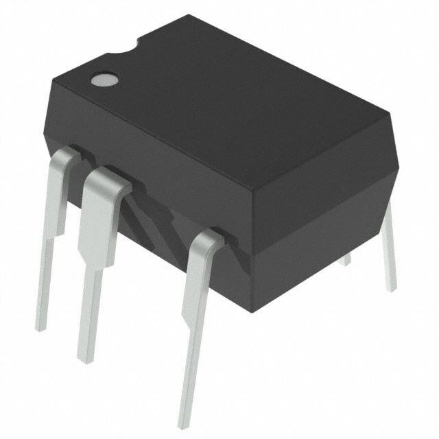
| 供应商器件封装 | DIP-8C |
| 其它名称 | 596-1233-5 |
| 功率(W) | 6.1W |
| 包装 | 管件 |
| 参考设计库 | http://www.digikey.com/rdl/4294959904/4294959863/271 |
| 封装/外壳 | 8-DIP(0.300",7.62mm),7 引线 |
| 工作温度 | -40°C ~ 150°C |
| 应用说明 | |
| 标准包装 | 50 |
| 特色产品 | http://www.digikey.com/cn/zh/ph/PI/lnkii.html |
| 电压-击穿 | 700V |
| 电压-输入 | - |
| 电压-输出 | - |
| 输出隔离 | 隔离 |
| 配用 | /product-detail/zh/RDK-158/596-1311-ND/2403328/product-detail/zh/RDK-160/596-1235-ND/1881310 |
| 频率范围 | 58kHz ~ 72kHz |


- 商务部:美国ITC正式对集成电路等产品启动337调查
- 曝三星4nm工艺存在良率问题 高通将骁龙8 Gen1或转产台积电
- 太阳诱电将投资9.5亿元在常州建新厂生产MLCC 预计2023年完工
- 英特尔发布欧洲新工厂建设计划 深化IDM 2.0 战略
- 台积电先进制程称霸业界 有大客户加持明年业绩稳了
- 达到5530亿美元!SIA预计今年全球半导体销售额将创下新高
- 英特尔拟将自动驾驶子公司Mobileye上市 估值或超500亿美元
- 三星加码芯片和SET,合并消费电子和移动部门,撤换高东真等 CEO
- 三星电子宣布重大人事变动 还合并消费电子和移动部门
- 海关总署:前11个月进口集成电路产品价值2.52万亿元 增长14.8%


PDF Datasheet 数据手册内容提取
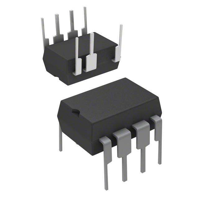
LNK603-606/613-616 LinkSwitch-II Family Energy-Efficient, Accurate CV/CC Switcher for Adapters and Chargers Product Highlights Dramatically Simplifies CV/CC Converters • Eliminates optocoupler and all secondary CV/CC control circuitry • Eliminates all control loop compensation circuitry Advanced Performance Features Wide Range • Compensates for transformer inductance tolerances High-Voltage • Compensates for input line voltage variations DC Input D • Compensates for cable voltage drop (LNK61X series) FB • Compensates for external component temperature variations LinkSwitch-II BP/M • Very tight IC parameter tolerances using proprietary trimming S technology • Frequency jittering greatly reduces EMI filter cost • Even tighter output tolerances achievable with external resistor PI-4960-012315 selection/trimming (a) Typical Application Schematic • Programmable switching frequency up to 85 kHz to reduce trans- former size V ±5% O Advanced Protection/Safety Features • Auto-restart protection reduces power delivered by >95% for output short-circuit and control loop faults (open and shorted components) • Hysteretic thermal shutdown – automatic recovery reduces power ±10% supply returns from the field • Meets high-voltage creepage requirements between DRAIN and all other pins both on the PCB and at the package EcoSmart™– Energy Efficient PI-4906-012315 I O • Easily meets all global energy efficiency regulations (b) Output Characteristic • No-load consumption below 30 mW at 230 VAC with optional Figure 1. Typical Application/Performance – Not a Simplified Circuit (a) and external bias winding Output Characteristic Envelope (b). (see Application Section for • ON/OFF control provides constant efficiency down to very light loads more information). – ideal for CEC and ENERGY STAR 2.0 regulations • No current sense resistors – maximizes efficiency Output Power Table Green Package 85-265 VAC • Halogen free and RoHS compliant package Product3 Adapter1 Open Frame2 Applications LNK603/613PG/DG 2.5 W 3.3 W • Chargers for cell/cordless phones, PDAs, MP3/portable audio devices, adapters, LED drivers, etc. LNK604/614PG/DG 3.5 W 4.1 W Description LNK605/615PG/DG 4.5 W 5.1 W LNK606/616PG/GG/DG 5.5 W 6.1 W The LinkSwitch™-II dramatically simplifies low power CV/CC charger designs by eliminating an optocoupler and secondary control circuitry. Table 1. Output Power Table. The device introduces a revolutionary control technique to provide very Notes: tight output voltage and current regulation, compensating for transformer 1. Minimum continuous power in a typical non-ventilated enclosed adapter and internal parameter tolerances along with input voltage variations. measured at +50 °C ambient, device, T <100 °C. J 2. Maximum practical continuous power in an open frame design with adequate The device incorporates a 700 V power MOSFET, a novel ON/OFF control heat sinking, measured at 50 °C ambient (see Key Applications Consider- state machine, a high-voltage switched current source for self biasing, ations section for more information). frequency jittering, cycle-by-cycle current limit and hysteretic thermal 3. Packages: P: DIP-8C, G: SMD-8C, D: SO-8C. shutdown circuitry onto a monolithic IC. DIP-8C (P Package) SMD-8C (G Package) SO-8C (D Package). Figure 2. Package Options. www.power.com August 2016 This Product is Covered by Patents and/or Pending Patent Applications.
LNK603-606/613-616 DRAIN (D) REGULATOR BYPASS 6 V (BP/M) + FB 6 V - + OUT Reset 5 V FEE(DFBBA)CK VTH - D Q MSATCAHTIENE V ILIMIT t SAMPLE-OUT I Drive LIM CABLE DROP VILIMIT DCMAX COMPENSATION FAULT 6.5 V FB Auto-Restart Open-Loop INDUCTANCE THERMAL CORRECTION SHUTDOWN tSAMPLE-INPUT DCMAX t SAMPLE SAMPLE-OUT t DELAY SAMPLE-INPUT OSCILLATOR SOURCE + (S) SOURCE CONSTANT ILIM - VILIMIT (S) CURRENT Current Limit Comparator LEADING EDGE BLANKING PI-4908-012915 Figure 3. Functional Block Diagram. Pin Functional Description DRAIN (D) Pin: P Package (DIP-8C) This pin is the power MOSFET drain connection. It provides internal G Package (SMD-8C) D Package (SO-8C) operating current for both start-up and steady-state operation. BYPASS/MULTI-FUNCTIONAL PROGRAMMABLE (BP/M) Pin: This pin has multiple functions: FB 1 8 S 1 8 FB S 1. It is the connection point for an external bypass capacitor for the internally generated 6 V supply. BP/M 2 7 S BP/M 2 7 S 2. It is a mode selection for the cable drop compensation for 6 LNK61X series. 6 S S 4 5 FEEDBACK (FB) Pin: D 4 5 S D S During normal operation, switching of the power MOSFET is controlled by this pin. This pin senses the AC voltage on the bias winding. This control input regulates both the output voltage in CV mode and output current in CC mode based on the flyback voltage of the bias winding. PI-3491-020615 The internal inductance correction circuit uses the forward voltage on the bias winding to sense the bulk capacitor voltage. Figure 4. Pin Configuration. SOURCE (S) Pin: This pin is internally connected to the output MOSFET source for high-voltage power and control circuit common returns. 2 Rev. J 08/16 www.power.com
LNK603-606/613-616 LinkSwitch-II Functional Description Auto-Restart and Open-Loop Protection In the event of a fault condition such as an output short or an open The LinkSwitch-II combines a high-voltage power MOSFET loop condition the LinkSwitch-II enters into an appropriate protection switch with a power supply controller in one device. Similar to the mode as described below. LinkSwitch-LP and TinySwitch-III it uses ON/OFF control to regulate the output voltage. In addition, the switching frequency is modulated In the event the FEEDBACK pin voltage during the flyback period falls to regulate the output current to provide a constant current below 0.7 V before the FEEDBACK pin sampling delay (~2.5 ms) for a characteristic. The LinkSwitch-II controller consists of an oscillator, duration in excess of ~450 ms (auto-restart on-time (t ) the AR-ON feedback (sense and logic) circuit, 6 V regulator, over-temperature converter enters into auto-restart, wherein the power MOSFET is protection, frequency jittering, current limit circuit, leading-edge disabled for 2 seconds (~18% auto-restart duty cycle). The auto- blanking, inductance correction circuitry, frequency control for restart alternately enables and disables the switching of the power constant current regulation and ON/OFF state machine for CV control. MOSFET until the fault condition is removed. Inductance Correction Circuitry In addition to the conditions for auto-restart described above, if the If the primary magnetizing inductance is either too high or low the sensed FEEDBACK pin current during the forward period of the converter will automatically compensate for this by adjusting the conduction cycle (switch “on” time) falls below 120 mA, the converter oscillator frequency. Since this controller is designed to operate in annunciates this as an open-loop condition (top resistor in potential discontinuous-conduction mode the output power is directly divider is open or missing) and reduces the auto-restart time from proportional to the set primary inductance and its tolerance can be 450 ms to approximately 6 clock cycles (90 ms), whilst keeping the completely compensated with adjustments to the switching disable period of 2 seconds. frequency. Over-Temperature Protection Constant Current (CC) Operation The thermal shutdown circuitry senses the die temperature. The As the output voltage and therefore the flyback voltage across the threshold is set at 142 °C typical with a 60 °C hysteresis. When the bias winding increases, the FEEDBACK pin voltage increases. The die temperature rises above this threshold (142 °C) the power switching frequency is adjusted as the FEEDBACK pin voltage MOSFET is disabled and remains disabled until the die temperature increases to provide a constant output current regulation. The falls by 60 °C, at which point the MOSFET is re-enabled. constant current circuit and the inductance correction circuit are Current Limit designed to operate concurrently in the CC region. The current limit circuit senses the current in the power MOSFET. Constant Voltage (CV) Operation When this current exceeds the internal threshold (I ), the power LIMIT As the FEEDBACK pin approaches V from the constant current MOSFET is turned off for the remainder of that cycle. The leading FBth regulation mode, the power supply transitions into CV operation. edge blanking circuit inhibits the current limit comparator for a short The switching frequency at this point is at its maximum value, time (t ) after the power MOSFET is turned on. This leading edge LEB corresponding to the peak power point of the CC/CV characteristic. blanking time has been set so that current spikes caused by The controller regulates the FEEDBACK pin voltage to remain at V capacitance and rectifier reverse recovery time will not cause FBth using an ON/OFF state-machine. The FEEDBACK pin voltage is premature termination of the MOSFET conduction. The LinkSwitch-II sampled 2.5 ms after the turn-off of the high-voltage switch. At light also contains a “di/dt” correction feature to minimize CC variation across loads the current limit is also reduced to decrease the transformer the input line range. flux density. 6.0 V Regulator Output Cable Compensation The 6 V regulator charges the bypass capacitor connected to the This compensation provides a constant output voltage at the end of BYPASS pin to 6 V by drawing a current from the voltage on the the cable over the entire load range in CV mode. As the converter DRAIN, whenever the MOSFET is off. The BYPASS pin is the internal load increases from no-load to the peak power point (transition point supply voltage node. When the MOSFET is on, the device runs off of between CV and CC) the voltage drop introduced across the output the energy stored in the bypass capacitor. Extremely low power cable is compensated by increasing the FEEDBACK pin reference consumption of the internal circuitry allows the LinkSwitch-II to voltage. The controller determines the output load and therefore the operate continuously from the current drawn from the DRAIN pin. correct degree of compensation based on the output of the state A bypass capacitor value of either 1 mF or 10 mF is sufficient for both machine. Cable drop compensation for a 24 AWG (0.3 W) cable is high frequency decoupling and energy storage. selected with C = 1 mF and for a 26 AWG (0.49 W) cable with BP C = 10 mF. PB 3 www.power.com Rev. J 08/16
LNK603-606/613-616 Applications Example C6 1 nF R7 100 V 200 Ω L1 T1 1.5 mH EE16 5 V, 555 mA 5 10 C3 D7 R2 820 pF SS14 D1 D2 470 kΩ 1 kV 3 8 R8 1N4007 1N4007 200 Ω 1 C7 DC 680 µF Output 10 V RF1 R3 VR1 8.2 Ω 300 Ω 2 2MM5230B-7 2 W 4.7 V D5 AC C1 C2 1N4007 4 Input 4.7 µF 4.7 µF 400 V 400 V R5 NC 13 kΩ 1% D6 LL4148 D D3 D4 LinkSwitch-II FB 1N4007 1N4007 U1 BP LNK613DG R4 S C4 6.2 kΩ C5 R6 8.87 kΩ 1 µF 10 µF 1% 25 V 16 V PI-5111-012315 Figure 5. Energy Efficient USB Charger Power Supply (74% Average Efficiency, <30 mW No-load Input Power). Circuit Description Table 2 shows the amount of compensation for each device and bypass capacitor value. The LNK60x devices do not provide cable This circuit shown in Figure 5 is configured as a primary-side drop compensation. regulated flyback power supply utilizing the LNK613DG. With an average efficiency of 74% and <30 mW no-load input power this The optional bias supply formed by D6 and C5 provides the operating design easily exceeds the most stringent current energy efficiency current for U1 via resistor R4. This reduces the no-load consumption requirements. from ~200 mW to <30 mW and also increases light load efficiency. Input Filter The rectified and filtered input voltage is applied to one side of the AC input power is rectified by diodes D1 through D4. The rectified primary winding of T1. The other side of the transformer’s primary DC is filtered by the bulk storage capacitors C1 and C2. Inductor L1, winding is driven by the integrated MOSFET in U1. The leakage C1 and C2 form a pi (π) filter, which attenuates conducted differential- inductance drain voltage spike is limited by an RCD-R clamp mode EMI noise. This configuration along with Power Integrations consisting of D5, R2, R3, and C3. transformer E-shield™ technology allow this design to meet EMI Output Rectification standard EN55022 class B with good margin without requiring a Y The secondary of the transformer is rectified by D7, a 1 A, 40 V capacitor, even with the output connected to safety earth ground. Schottky barrier type for higher efficiency, and filtered by C7. If Fusible resistor RF1 provides protection against catastrophic failure. lower efficiency is acceptable then this can be replaced with a This should be suitably rated (typically a wire wound type) to 1 A PN junction diode for lower cost. In this application C7 was sized withstand the instantaneous dissipation while the input capacitors to meet the required output voltage ripple specification without charge when first connected to the AC line. requiring a post LC filter. To meet battery self discharge requirement LNK 613 Primary the pre-load resistor has been replaced with a series resistor and The LNK613DG device (U1) incorporates the power switching device, Zener network (R8 and VR1). However in designs where this is not a oscillator, CC/CV control engine, startup, and protection functions. requirement a standard 1 kW resistor can be used. The integrated 700 V MOSFET provides a large drain voltage margin Output Regulation in universal input AC applications, increasing reliability and also The LNK613 regulates the output using ON/OFF control in the reducing the output diode voltage stress by allowing a greater constant voltage (CV) regulation region of the output character-istic and transformer turns ratio. The device is completely self-powered from frequency control for constant current (CC) regulation. The feedback the BYPASS pin and decoupling capacitor C4. For the LNK61X resistors (R5 and R6) were selected using standard 1% resistor devices, the bypass capacitor value also selects the amount of output values to center both the nominal output voltage and constant cable voltage drop compensation. A 1 mF value selects the standard current regulation thresholds. compensation. A 10 mF value selects the enhanced compensation. 4 Rev. J 08/16 www.power.com
LNK603-606/613-616 Key Application Considerations LinkSwitch-II Output Cable Voltage Drop Output Power Table Compensation The data sheet maximum output power table (Table 1) repre-sents Device BYPASS Pin Output Voltage Capacitor Value Change Factor the maximum practical continuous output power level that can be obtained under the following assumed conditions: 1 mF 1.035 LNK613 10 mF 1.055 1. The minimum DC input voltage is 90 V or higher at 85 VAC input. The value of the input capacitance should be large enough to 1 mF 1.045 LNK614 meet these criteria for AC input designs. 10 mF 1.065 2. Secondary output of 5 V with a Schottky rectifier diode. 1 mF 1.050 3. Assumed efficiency of 70%. LNK615 4. Discontinuous mode operation (K >1.3). 10 mF 1.070 P 5. The part is board mounted with SOURCE pins soldered to a 1 mF 1.060 sufficient area of copper to keep the SOURCE pin temperature at LNK616 10 mF 1.090 or below 90 °C. 6. Ambient temperature of 50 °C for open frame designs and an Table 2. Cable Compensation Change Factor vs. Device and BYPASS Pin Capacitor Value. internal enclosure temperature of 60 °C for adapter designs. Note: Higher output power are achievable if an output CC tolerance of the power supply. See Figure 6 for a recommended circuit board >±10% is acceptable, allowing the device to be operated at a higher layout for LinkSwitch-II. SOURCE pin temperature. When designing a printed circuit board for the LinkSwitch-II based Output Tolerance power supply, it is important to follow the following guidelines: LinkSwitch-II provides an overall output tolerance (including line, Single Point Grounding component variation and temperature) of ±5% for the output voltage Use a single point (Kelvin) connection at the negative terminal of the in CV operation and ±10% for the output current during CC operation input filter capacitor for the LinkSwitch-II SOURCE pin and bias over a junction temperature range of 0 °C to 100 °C for the P/G winding return. This improves surge capabilities by returning surge package. For the D package (SO8) additional CC variance may occur currents from the bias winding directly to the input filter capacitor. due to stress caused by the manufacturing flow (i.e. solder-wave immersion or IR reflow). A sample power supply build is Bypass Capacitor recommended to verify production tolerances for each design. The BYPASS pin capacitor should be located as close as possible to the SOURCE and BYPASS pins. BYPASS Pin Capacitor Selection Feedback Resistors For LinkSwitch-II 60x Family of Devices (without output Place the feedback resistors directly at the FEEDBACK pin of the cable voltage drop compensation) LinkSwitch-II device. This minimizes noise coupling. A 1 mF BYPASS pin capacitor is recommended. The capacitor voltage Thermal Considerations rating should be greater than 7 V. The capacitor’s dielectric material The copper area connected to the SOURCE pins provides the is not important but tolerance of capacitor should be ≤ ±50%. The LinkSwitch-II heat sink. A good estimate is that the LinkSwitch-II will capacitor must be physically located close to the LinkSwitch-II dissipate 10% of the output power. Provide enough copper area to BYPASS pin. keep the SOURCE pin temperature below 90 °C. Higher temperatures For LinkSwitch-II 61x Family of Devices (with output cable are allowable only if an output current (CC) tolerance above ±10% is voltage drop compensation) acceptable. In this case a maximum SOURCE pin temperature below The amount of output cable compensation can be selected with the 110 °C is recommended to provide margin for part to part R DS(ON) value of the BYPASS pin capacitor. A value of 1 mF selects the variation. standard cable compensation. A 10 mF capacitor selects the enhanced Secondary Loop Area cable compensation. Table 2 shows the amount of compensation for To minimize leakage inductance and EMI the area of the loop connecting each LinkSwitch-II device and capacitor value. The capacitor can be the secondary winding, the output diode and the output filter capacitor either ceramic or electrolytic but tolerance and temperature variation should be minimized. In addition, sufficient copper area should be should be ≤ ±50%. provided at the anode and cathode terminal of the diode for heat The output voltage that is entered into PIXls design spreadsheet is sinking. A larger area is preferred at the quiet cathode terminal. the voltage at the end of the output cable when the power supply is A large anode area can increase high frequency radiated EMI. delivering maximum power. The output voltage at the terminals of Electrostatic Discharge Spark Gap the supply is the value measured at the end of the cable multiplied by An trace is placed along the isolation barrier to form one electrode of the output voltage change factor. a spark gap. The other electrode on the secondary is formed by the LinkSwitch-II Layout Considerations output return node. The spark gap directs ESD energy from the secondary back to the AC input. The trace from the AC input to the Circuit Board Layout spark gap electrode should be spaced away from other traces to LinkSwitch-II is a highly integrated power supply solution that prevent unwanted arcing occurring and possible circuit damage. integrates on a single die, both, the controller and the high-voltage MOSFET. The presence of high switching currents and voltages Drain Clamp Optimization together with analog signals makes it especially important to follow LinkSwitch-II senses the feedback winding on the primary side to good PCB design practice to ensure stable and trouble free operation regulate the output. The voltage that appears on the feed-back 5 www.power.com Rev. J 08/16
LNK603-606/613-616 Output Filter Input Stage Primary Clamp Output Capacitors Diode Snubber C1 R1 T1 R8 C6 C2 R4 R3 S SC3S S D5 D7 R1 LinkSwitch-II L2 U1 R5 R2 Feedback D1 Resistors R6 FB BP D C7 D2 C4 D4 C5 Bypass D3 C8 Capacitor R9 Bypass Supply D3 Components RF1 Preload Resistor AC Spark Input Gap DC Output PI-5110-012315 Figure 6. PCB Layout Example Showing 5.1 W Design using P Package. winding is a reflection of the secondary winding voltage while the exceed 3 mA at the maximum bias winding voltage. The value of R4 is internal MOSFET is off. Therefore any leakage inductance induced calculated according to (V – V )/I , where V (10 V typ.) is the BIAS BP S2 BIAS ringing can affect output regulation. Optimizing the drain clamp to voltage across C5, I (0.5 mA typ.) is the IC supply current and V S2 BP minimize the high frequency ringing will give the best regulation. (6.0 V typ.) is the BYPASS pin voltage. The parameters I and V are S2 BP Figure 7 shows the desired drain voltage waveform compared to provided in the parameter table of the LinkSwitch-II data sheet. Diode Figure 8 with a large undershoot due to the leakage inductance D6 can be any low cost diode such as FR102, 1N4148 or BAV19/20/21. induced ring. This will reduce the output voltage regulation perfor- Quick Design Checklist mance. To reduce this adjust the value of the resistor in series with the clamp diode. As with any power supply design, all LinkSwitch-II designs should be verified on the bench to make sure that component specifications are Addition of a Bias Circuit for Higher Light Load Efficiency and not exceeded under worst-case conditions. The following minimum Lower No-load Input Power Consumption. set of tests is strongly recommended: The addition of a bias circuit can decrease the no-load input power 1. Maximum drain voltage – Verify that peak V does not exceed 680 V from ~200 mW down to less than 30 mW at 230 VAC input. Light DS at the highest input voltage and maximum output power. load efficiency also increases which may avoid the need to use a 2. Maximum drain current – At maximum ambient temperature, Schottky barrier vs PN junction output diode while still meeting maximum input voltage and maximum output load, verify drain average efficiency requirements. current waveforms at start-up for any signs of transformer The power supply schematic shown in Figure 5 has the bias circuit saturation and excessive leading edge current spikes. LinkSwitch-II incorporated. Diode D6, C5 and R4 form the bias circuit. As the has a leading edge blanking time of 170 ns to prevent premature output voltage is less than 8 V, an additional transformer winding is termination of the ON-cycle. needed, AC stacked on top of the feedback winding. This provides a 3. Thermal check – At maximum output power, both minimum and high enough voltage to supply the BYPASS pin even during low maximum input voltage and maximum ambient temperature; switching frequency operation at no-load. verify that temperature specifications are not exceeded for LinkSwitch-II, transformer, output diodes and output capacitors. In Figure 5 the additional bias winding (from pin 2 to pin 1) is stacked Enough thermal margin should be allowed for part-to-part on top of the feedback winding (pin 4 to pin 2). Diode D6 rectifies variation of the R of LinkSwitch-II, as specified in the data the output and C5 is the filter capacitor. A 10 uF capacitor is DS(ON) sheet. To assure 10% CC tolerance a maximum SOURCE pin recommended to hold up the bias voltage at low switching frequencies. temperature of 90 ºC is recommended. The capacitor type is not critical but the voltage rating should be above the maximum value of V . The recommended current into Design Tools BIAS the BYPASS pin is equal to IC supply current (~0.5 mA) at the Up-to-date information on design tools can be found at the Power minimum bias winding voltage. The BYPASS pin current should not Integrations web site: www.power.com 6 Rev. J 08/16 www.power.com
LNK603-606/613-616 An overshoot PI-5093-012315 PI-5094-012315 is acceptable Negative ring may increase output ripple and/or degrade output regulation Figure 7. Desired Drain Voltage Waveform with Minimal Leakage Figure 8. Undesirable Drain Voltage Waveform with Large Leakage Ringing Undershoot. Ring Undershoot. L1 TI 1 mH EE13 5 10 C3 D7 R2 820 pF SL13 D1 D2 470 kΩ 1 kV 3 8 1N4007 1N4007 C7 DC 470 µF 1 kΩ Output 10 V RF1 R3 8.2 Ω 300 Ω 2 2 W D5 AC C1 C2 1N4007 4 Input 4.7 µF 4.7 µF 400 V 400 V NC R5 13 kΩ 1% D D3 D4 LinkSwitch-II FB 1N4007 1N4007 U1 BP LNK613DG S C4 R6 1 µF 9.31 kΩ 50 V 1% PI-5116-012315 Figure 9. LinkSwitch-II Flyback Power Supply without Bias Supply. 7 www.power.com Rev. J 08/16
LNK603-606/613-616 Absolute Maximum Ratings1,5 DRAIN Voltage ........................................................-0.3 V to 700 V Lead Temperature(3) .................................................................260 °C DRAIN Peak Current: LNK603/613 ..............................320 (480) mA4 Notes: LNK604/614 ..............................400 (600) mA4 1. All voltages referenced to SOURCE, T = 25 °C. A LNK605/615 ..............................504 (750) mA4 2. Duration not to exceed 2 ms. LNK606/616 ..............................654 (980) mA4 3. 1/16 in. from case for 5 seconds. Peak Negative Pulsed Drain Current ...................................-100 mA2 4. The higher peak DRAIN current is allowed while the DRAIN FEEDBACK Pin Voltage .................................................-0.3 V to 9 V voltage is simultaneously less than 400 V. FEEDBACK Pin Current ........................................................100 mA 5. Maximum ratings specified may be applied, one at a time BYPASS Pin Voltage ......................................................-0.3 V to 9 V without causing permanent damage to the product. BYPASS Pin Current ...............................................................10 mA Exposure to Absolute Maximum ratings for extended Storage Temperature ...................................... ..........-65 °C to 150 °C periods of time may affect product reliability. Operating Junction Temperature ..............................-40 °C to 150 °C Thermal Resistance Thermal Resistance: P or G Package: Notes: (q ) .......................... ..............70 °C/W2; 60 °C/W3 1. Measured on pin 8 (SOURCE) close to plastic interface. JA (q )1 ......................................................11 °C/W 2. Soldered to 0.36 sq. in. (232 mm2), 2 oz. (610 g/m2) copper clad. JC D Package: 3. Soldered to 1 sq. in. (645 mm2), 2 oz. (610 g/m2) copper clad. (q ) ......................................100 °C/W2; 80 °C/W3 JA (q )1 .......................................................30 °C/W JC Conditions Parameter Symbol SOURCE = 0 V; T = 0 to 100 °C Min Typ Max Units J (Unless Otherwise Specified) Control Functions T = 25 °C, V = V LNK603/6 59 66 73 J FB FBth Output Frequency f t × I = 2 mA-ms kHz OSC ON FB See Notes A, G LNK613/6 58 65 72 Frequency Ratio T = 25 °C f J 1.59 1.635 1.68 (Constant Current) RATIO(CC) Between V = 1.0 V and V = 1.6 V FB FB Frequency Ratio Between t × I = 1.6 mA × ms f ON FB 1.160 1.215 1.265 (Inductance Correction) RATIO(IC) and t × I = 2 mA × ms ON FB Peak-Peak Jitter Compared to Frequency Jitter ±7 % Average Frequency, T = 25 °C J Ratio of Output Fre- T = 25 °C f J 12 16.5 21 % quency at Auto-Restart OSC(AR) Relative to f OSC Maximum Duty Cycle DC See Notes D, E 55 % MAX LNK603/604P 1.815 1.840 1.865 LNK603/604D 1.855 1.880 1.905 LNK605P, LNK605D 1.835 1.860 1.885 T = 25 °C J LNK606P/G/D 1.775 1.800 1.825 FEEDBACK Pin Voltage V C = 10 mF V FBth BP LNK613/614P 1.935 1.960 1.985 See Note F LNK613/614/615D 1.975 2.000 2.025 LNK615P 1.975 2.000 2.025 LNK616P/G/D 1.935 1.960 1.985 FEEDBACK Pin Voltage TC -0.01 %/°C Temperature Coefficient VFB FEEDBACK Pin Voltage V 0.65 0.72 0.79 V at Turn-OFF Threshold FB(AR) Cable Compensation υ LNK613 CBP = 1 mF 1.035 Factor FB C = 10 mF 1.055 BP 8 Rev. J 08/16 www.power.com
LNK603-606/613-616 Conditions Parameter Symbol SOURCE = 0 V; T = 0 to 100 °C Min Typ Max Units J (Unless Otherwise Specified) Control Functions C = 1 mF 1.045 LNK614 BP C = 10 mF 1.065 BP Cable Compensation υ LNK615 CBP = 1 mF 1.05 Factor FB C = 10 mF 1.07 BP C = 1 mF 1.06 LNK616 BP C = 10 mF 1.09 BP I = -500 mA 4 FB f = 66 kHz OSC I = -1 mA 2 Switch ON-Time t V = V FB ms ON FB FBth I = -1.5 mA 1.33 See Note E FB I = -2 mA 1 FB Minimum Switch t See Note E 700 ns ON-Time ON(min) FEEDBACK Pin t 2.35 2.55 2.75 ms Sampling Delay FB I FB Voltage > V 280 330 S1 FBth DRAIN Supply LNK6X3/4 440 520 FB Voltage = V -0.1, mA Current FBth I Switch ON-Time = t LNK6X5 480 560 S2 ON (MOSFET Switching at f ) OSC LNK6X6 520 600 LNK6X3/4 -5.0 -3.4 -1.8 I V = 0 V BYPASS Pin CH1 BP LNK6X5/6 -7.0 -4.8 -2.5 mA Charge Current LNK6X3/4 -4.0 -2.3 -1.0 I V = 4 V CH2 BP LNK6X5/6 -5.6 -3.2 -1.4 BYPASS Pin Voltage V 5.65 6.00 6.25 V BP BYPASS Pin V 0.70 1.00 1.20 V Voltage Hysteresis BPH BYPASS Pin V 6.2 6.5 6.8 V Shunt Voltage SHUNT Circuit Protection LNK6X3 186 200 214 di/dt = 50 mA/ms , T = 25 °C J LNK6X4 233 250 267 di/dt = 60 mA/ms , T = 25 °C J Current Limit I mA LIMIT LNK6X5 293 315 337 di/dt = 70 mA/ms , T = 25 °C J LNK6X6 382 410 438 di/dt = 100 mA/ms , T = 25 °C J Normalized Output T = 25 °C I J 0.975 1.000 1.025 Current O See Figure 20, See Note F Leading Edge T = 25 °C t J 170 215 ns Blanking Time LEB See Note E Thermal Shutdown T 135 142 150 °C Temperature SD 9 www.power.com Rev. J 08/16
LNK603-606/613-616 Conditions Parameter Symbol SOURCE = 0 V; T = 0 to 100 °C Min Typ Max Units J (Unless Otherwise Specified) Circuit Protection Thermal Shutdown T 60 °C Hysteresis SDH Output T = 25 °C 24 28 LNK6X3 J I = 50 mA D T = 100 °C 36 42 J T = 25 °C 24 28 LNK6X4 J I = 50 mA ON-State D TJ = 100 °C 36 42 R W Resistance DS(ON) T = 25 °C 16 19 LNK6X5 J I = 62 mA D T = 100 °C 24 28 J T = 25 °C 9.6 11 LNK6X6 J I = 82 mA D T = 100 °C 14 17 J V = 560 V, See Figure 20 I DS 50 OFF-State DSS1 T = 125 °C, See Note C J mA Leakage V = 375 V, See Figure 20 I DS 15 DSS2 T = 50 °C J Breakdown T = 25 °C BV J 700 V Voltage DSS See Figure 20 DRAIN Supply 50 V Voltage t × I = 2 mA-ms, f = 12 kHz Auto-Restart ON FB OSC t V = 0 450 ms ON-Time AR-ON FB See Notes A, E Auto-Restart OFF-Time t 1.2 2 s AR-OFF Open-Loop FEEDBACK I See Note E -120 mA Pin Current Threshold OL Open-Loop ON-Time See Note E 90 ms NOTES: A. Auto-restart ON-time is a function of switching frequency programmed by t × I and minimum frequency in CC mode. on FB B. The current limit threshold is compensated to cancel the effect of current limit delay. As a result the output current stays constant across the input line range. C. I is the worst-case OFF-state leakage specification at 80% of BV and maximum operating junction temperature. I is a typical DSS1 DSS DSS2 specification under worst-case application conditions (rectified 265 VAC) for no-load consumption calculations. D. When the duty-cycle exceeds DC the LinkSwitch-II operates in on-time extension mode. MAX E. This parameter is derived from characterization. F. Mechanical stress induced during the assembly may cause shift in this parameter. This shift has no impact on the ability of LinkSwitch-II to meet CC = ±10% and CV = ±5% in mass production given the design follows recommendation in AN-44 and good manufacturing practice. G. The switching frequency is programmable between 60 kHz and 85 kHz. 10 Rev. J 08/16 www.power.com
LNK603-606/613-616 Typical Performance Characteristics 1.200 1.200 °C)1.000 PI-5085-012315 °C)1.000 PI-5086-012315 t5 0.800 5 0.800 Limito 2 ncyto 2 nt ed 0.600 ueed 0.600 ez qz urrmali0.400 Fremali0.400 C r r o o N N (0.200 (0.200 0.000 0.000 -40 -15 10 35 60 85 110 135 -40 -15 10 35 60 85 110 135 Temperature (°C) Temperature (°C) Figure 10. Current Limit vs. Temperature. Figure 11. Output Frequency vs. Temperature. Ratioo 25 °C)101...280000000 PI-5087-012315 Ratioo 25 °C)101...280000000 PI-5088-012315 cy d t0.600 cy d t0.600 ne ne equemaliz0.400 equemaliz0.400 Fror Fror N N (0.200 (0.200 0.000 0.000 -40 -15 10 35 60 85 110 135 -40 -15 10 35 60 85 110 135 Temperature (°C) Temperature (°C) Figure 12. Frequency Ratio vs. Temperature (Constant Current). Figure 13. Frequency Ratio vs. Temperature (Inductor Current). 1.200 1.200 e°C)1.000 PI-5089-012315 urrent°C)1.000 PI-5090-012315 back Voltagalized to 25 00..680000 ed Output Calized to 25 00..680000 dm0.400 zm0.400 FeeNor maliNor (0.200 or(0.200 N 0.000 0.000 -40 -15 10 35 60 85 110 135 -40 -15 10 35 60 85 110 135 Temperature (°C) Temperature (°C) Figure 14. Feedback Voltage vs. Temperature. Figure 15. Normalized Output Current vs. Temperature. 11 www.power.com Rev. J 08/16
LNK603-606/613-616 Typical Performance Characteristics (cont.) geC)°1.1 PI-2213-012315 A) 320500 TTCCAASSEE == 2150 0° C°C PI-5082-012315 a5 m wn Volted to 21.0 rrent ( 210500 BreakdoNormaliz Drain Cu 100 LSNcaKl6inxg3 Fact1o.r0s: ( 50 LNK6x4 1.0 LNK6x5 1.5 LNK6x6 2.5 0.9 0 -50 -25 0 25 50 75 100 125 150 0 2 4 6 8 10 Junction Temperature (°C) DRAIN Voltage (V) Figure 16. Breakdown vs. Temperature. Figure 17. Output Characteristic. (pF) 1000 PI-5083-012315 5400 Scaling Factors: PI-5084-012315 ce 100 W) LLNNKK66xx34 11..00 an Scaling Factors: m 30 LNK6x5 1.5 n Capacit 10 LLLLNNNNKKKK6666xxxx3456 1112....0055 Power ( 20 LNK6x6 2.5 ai r 10 D 1 0 0 100 200 300 400 500 600 0 200 400 600 Drain Voltage (V) DRAIN Voltage (V) Figure 18. C vs. Drain Voltage. Figure 19. Drain Capacitance Power. OSS 12 Rev. J 08/16 www.power.com
LNK603-606/613-616 LinkSwitch-II FB S 1 µF BP/M S 5 µF 50 kΩ 10 kΩ .1 µF S D S 4 kΩ S1 S2 V IN + 16 V Curve Tracer To measure BV , I , and I follow these steps: DSS DSS1 DSS2 1) Close S1, open S2. 2) Power-up V source (16 V). IN 3) Open S1, close S2. 4) Measure I/V characteristics of DRAIN pin using the curve tracer. PI-4962-012915 Figure 20. Test Set-up for Leakage and Breakdown Tests. 3.3 V 470 pF 200 V 680 µF + RO VO 200 Ω 11.5 kΩ + 50 V LinkSwitch-II FB S BP S 7.15 kΩ S 10 µF D S 1) The transformer inductance is chosen to set the value of t × I to 2 mA × µS. ON FB 2) R is chosen to operate test circuit in the CC region. O 3) V is measured. O 4) Output current is V / R . O O PI-4963-012315 Figure 21. Test Set-up for Output Current Measurements. 13 www.power.com Rev. J 08/16
LNK603-606/613-616 PDIP-8C (P Package) ⊕D S.004 (.10) Notes: -E- 1. Package dimensions conform to JEDEC specification MS-001-AB (Issue B 7/85) for standard dual-in-line (DIP) package with .300 inch row spacing. 2. Controlling dimensions are inches. Millimeter sizes are shown in parentheses. .240 (6.10) 3. Dimensions shown do not include mold flash or other .260 (6.60) protrusions. Mold flash or protrusions shall not exceed .006 (.15) on any side. 4. Pin locations start with Pin 1, and continue counter-clock- wise to Pin 8 when viewed from the top. The notch and/or dimple are aids in locating Pin 1. Pin 3 is omitted. Pin 1 5. Minimum metal to metal spacing at the package body for the omitted lead location is .137 inch (3.48 mm). .356 (9.05) -D- 6. Lead width measured at package body. .387 (9.83) 7. Lead spacing measured with the leads constrained to be .057 (1.45) perpendicular to plane T. .068 (1.73) (NOTE 6) .125 (3.18) .015 (.38) .145 (3.68) MINIMUM -T- SEATING .008 (.20) PLANE .118 (3.00) .015 (.38) .140 (3.56) .300 (7.62) BSC .100 (2.54) BSC .048 (1.22) .137 (3.48) (NOTE 7) .053 (1.35) MINIMUM P08C .014 (.36) .300 (7.62) .022 (.56) ⊕T E D S .010 (.25) M .390 (9.91) PI-3933-081716 14 Rev. J 08/16 www.power.com
LNK603-606/613-616 SMD-8C (G Package) Notes: ⊕D S.004 (.10) .046.060 .060.046 1. Controlling dimensions are inches. Millimeter sizes are -E- shown in parentheses. .080 2. Dimensions shown do not include mold flash or other protrusions. Mold flash or .086 protrusions shall not exceed .372 (9.45) .186 .006 (.15) on any side. .240 (6.10) 3. Pin locations start with Pin 1, .260 (6.60) .388 (9.86) .286 .420 and continue counter-clock- ⊕E S .010 (.25) wise to Pin 8 when viewed from the top. Pin 3 is omitted. 4. Minimum metal to metal spacing at the package body for the omitted lead location is .137 inch (3.48 mm). Pin 1 Pin 1 5. Lead width measured at .137 (3.48) package body. MINIMUM Solder Pad Dimensions 6. D and E are referenced .100 (2.54) (BSC) datums on the package body. .356 (9.05) -D- .387 (9.83) .057 (1.45) .125 (3.18) .068 (1.73) .145 (3.68) (NOTE 5) .004 (.10) .032 (.81) .048 (1.22) .037 (.94) .053 (1.35) .009 (.23) .004 (.10) .036 (0.91) 0 °-8° G08C .012 (.30) .044 (1.12) PI-4015-081716 15 www.power.com Rev. J 08/16
LNK603-606/613-616 SO-8C (D Package) 0.10 (0.004) C A-B2X 2 DETAIL A 4 B 4.90 (0.193) BSC A 4 D 8 5 GAUGE PLANE SEATING PLANE 2 3.90 (0.154) BSC 6.00 (0.236) BSC C 0 - 8o 0.25 (0.010) 1.04 (0.041) REF BSC 0.10 (0.004) C D 0.40 (0.016) 2X Pin 1 ID 1 4 0.20 (0.008) C 1.27 (0.050) 1.27 (0.050) BSC 2X 7X 0.31 - 0.51 (0.012 - 0.020) 0.25 (0.010) M CA-BD 1.35 (0.053) 1.25 - 1.65 DETAIL A 1.75 (0.069) (0.049 - 0.065) 0.10 (0.004) 0.10 (0.004) C H 0.25 (0.010) 7X SEATING PLANE 0.17 (0.007) C 0.25 (0.010) Reference Solder Pad + Dimensions Notes: 1. JEDEC reference: MS-012. 2.00 (0.079) 4.90 (0.193) 2. Package outline exclusive of mold flash and metal burr. 3. Package outline inclusive of plating thickness. 4. Datums A and B to be determined at datum plane H. + + + 5. Controlling dimensions are in millimeters. Inch dimensions are shown in parenthesis. Angles in degrees. D07C 1.27 (0.050) 0.60 (0.024) PI-4526-012315 Part Ordering Information • LinkSwitch Product Family • II Series Number • Package Identifier G Plastic Surface Mount DIP P Plastic DIP D Plastic SO-8 • Package Material G GREEN: Halogen Free and RoHS Compliant • Tape & Reel and Other Options Blank Standard Configurations LNK 615 D G - TL TL Tape & Reel, 1 k pcs minimum for G Package. 2.5 k pcs for D Package. Not available for P Package. 16 Rev. J 08/16 www.power.com
LNK603-606/613-616 Revision Notes Date C Final data sheet. 06/08 D Auto-restart time modified PCN-09131. 03/09 E Introduced Max Current Limit when V DRAIN is below 400 V. 07/09 F Added LNK616DG and LNK606DG. 01/10 G Updated Note 6 in Parameter Table. 02/10 H Updated due to DM process change. 05/13 H Specified Max BYPASS Pin Current. 03/14 I Figure removed “Test Set-up for FEEDBACK Pin Measurements” from previous version. Updated to latest Brand Style. 02/15 J Updated PDIP-8C (P Package) and SMD-8C (G Package) per PCN-16232. 08/16 17 www.power.com Rev. J 08/16
For the latest updates, visit our website: www.power.com Power Integrations reserves the right to make changes to its products at any time to improve reliability or manufacturability. Power Integrations does not assume any liability arising from the use of any device or circuit described herein. POWER INTEGRATIONS MAKES NO WARRANTY HEREIN AND SPECIFICALLY DISCLAIMS ALL WARRANTIES INCLUDING, WITHOUT LIMITATION, THE IMPLIED WARRANTIES OF MERCHANTABILITY, FITNESS FOR A PARTICULAR PURPOSE, AND NON-INFRINGEMENT OF THIRD PARTY RIGHTS. Patent Information The products and applications illustrated herein (including transformer construction and circuits external to the products) may be covered by one or more U.S. and foreign patents, or potentially by pending U.S. and foreign patent applications assigned to Power Integrations. A complete list of Power Integrations patents may be found at www.power.com. Power Integrations grants its customers a license under certain patent rights as set forth at http://www.power.com/ip.htm. Life Support Policy POWER INTEGRATIONS PRODUCTS ARE NOT AUTHORIZED FOR USE AS CRITICAL COMPONENTS IN LIFE SUPPORT DEVICES OR SYSTEMS WITHOUT THE EXPRESS WRITTEN APPROVAL OF THE PRESIDENT OF POWER INTEGRATIONS. As used herein: 1. A Life support device or system is one which, (i) is intended for surgical implant into the body, or (ii) supports or sustains life, and (iii) whose failure to perform, when properly used in accordance with instructions for use, can be reasonably expected to result in significant injury or death to the user. 2. A critical component is any component of a life support device or system whose failure to perform can be reasonably expected to cause the failure of the life support device or system, or to affect its safety or effectiveness. The PI logo, TOPSwitch, TinySwitch, SENZero, SCALE-iDriver, Qspeed, PeakSwitch, LYTSwitch, LinkZero, LinkSwitch, InnoSwitch, HiperTFS, HiperPFS, HiperLCS, DPA-Switch, CAPZero, Clampless, EcoSmart, E-Shield, Filterfuse, FluxLink, StakFET, PI Expert and PI FACTS are trademarks of Power Integrations, Inc. Other trademarks are property of their respective companies. ©2016, Power Integrations, Inc. Power Integrations Worldwide Sales Support Locations World Headquarters Germany Italy Singapore 5245 Hellyer Avenue Lindwurmstrasse 114 Via Milanese 20, 3rd. Fl. 51 Newton Road San Jose, CA 95138, USA. 80337 Munich 20099 Sesto San Giovanni (MI) Italy #19-01/05 Goldhill Plaza Main: +1-408-414-9200 Germany Phone: +39-024-550-8701 Singapore, 308900 Customer Service: Phone: +49-895-527-39110 Fax: +39-028-928-6009 Phone: +65-6358-2160 Phone: +1-408-414-9665 Fax: +49-895-527-39200 e-mail: eurosales@power.com Fax: +65-6358-2015 Fax: +1-408-414-9765 e-mail: eurosales@power.com e-mail: singaporesales@power.com Japan e-mail: usasales@power.com Germany Kosei Dai-3 Bldg. Taiwan China (Shanghai) HellwegForum 1 2-12-11, Shin-Yokohama, 5F, No. 318, Nei Hu Rd., Sec. 1 Rm 2410, Charity Plaza, No. 88 59469 Ense Kohoku-ku Nei Hu Dist. North Caoxi Road Germany Yokohama-shi, Kanagawa Taipei 11493, Taiwan R.O.C. Shanghai, PRC 200030 Tel: +49-2938-64-39990 222-0033 Japan Phone: +886-2-2659-4570 Phone: +86-21-6354-6323 e-mail: igbt-driver.sales@ Phone: +81-45-471-1021 Fax: +886-2-2659-4550 Fax: +86-21-6354-6325 power.com Fax: +81-45-471-3717 e-mail: taiwansales@power.com e-mail: chinasales@power.com e-mail: japansales@power.com India UK China (Shenzhen) #1, 14th Main Road Korea Cambridge Semiconductor, 17/F, Hivac Building, No. 2, Keji Nan Vasanthanagar RM 602, 6FL a Power Integrations company 8th Road, Nanshan District, Bangalore-560052 India Korea City Air Terminal B/D, 159-6 Westbrook Centre, Block 5, 2nd Floor Shenzhen, China, 518057 Phone: +91-80-4113-8020 Samsung-Dong, Kangnam-Gu, Milton Road Phone: +86-755-8672-8689 Fax: +91-80-4113-8023 Seoul, 135-728, Korea Cambridge CB4 1YG Fax: +86-755-8672-8690 e-mail: indiasales@power.com Phone: +82-2-2016-6610 Phone: +44 (0) 1223-446483 e-mail: chinasales@power.com Fax: +82-2-2016-6630 e-mail: eurosales@power.com e-mail: koreasales@power.com
Mouser Electronics Authorized Distributor Click to View Pricing, Inventory, Delivery & Lifecycle Information: P ower Integrations: LNK603DG LNK613DG LNK604DG LNK614DG LNK605DG LNK615DG LNK606GG LNK616GG LNK606DG LNK606DG-TL LNK616DG LNK616DG-TL LNK604PG LNK606PG LNK613PG LNK614DG-TL LNK605DG-TL LNK604DG-TL LNK603DG-TL LNK606GG-TL LNK615DG-TL LNK603PG LNK613DG-TL LNK616GG-TL LNK615PG LNK616PG LNK614PG LNK605PG