ICGOO在线商城 > 集成电路(IC) > 时钟/计时 - 时钟发生器,PLL,频率合成器 > LMK02002ISQ/NOPB

 Datasheet下载
- 型号: LMK02002ISQ/NOPB
- 制造商: Texas Instruments
- 库位|库存: xxxx|xxxx
- 要求:
| 数量阶梯 | 香港交货 | 国内含税 |
| +xxxx | $xxxx | ¥xxxx |
查看当月历史价格
查看今年历史价格
LMK02002ISQ/NOPB产品简介:
ICGOO电子元器件商城为您提供LMK02002ISQ/NOPB由Texas Instruments设计生产,在icgoo商城现货销售,并且可以通过原厂、代理商等渠道进行代购。 LMK02002ISQ/NOPB价格参考¥60.31-¥100.59。Texas InstrumentsLMK02002ISQ/NOPB封装/规格:时钟/计时 - 时钟发生器,PLL,频率合成器, 。您可以下载LMK02002ISQ/NOPB参考资料、Datasheet数据手册功能说明书,资料中有LMK02002ISQ/NOPB 详细功能的应用电路图电压和使用方法及教程。
LMK02002ISQ/NOPB 是 Texas Instruments(德州仪器)推出的一款高性能时钟发生器、锁相环(PLL)和频率合成器芯片,广泛应用于需要高精度时钟信号的电子系统中。

其主要应用场景包括:

1. 通信设备:如无线基站、光模块、传输设备等,用于生成稳定的高频时钟信号,确保数据传输的准确性和稳定性。

2. 测试与测量仪器:如示波器、频谱分析仪等,提供精确的参考时钟,提高测量精度。

3. 工业控制系统:在高精度运动控制或同步系统中,为系统提供低抖动、高稳定性的时钟源。

4. 音频/视频设备:用于高端音视频系统中,减少时钟抖动对音视频质量的影响,提升播放效果。

5. 网络设备:如路由器、交换机等,用于同步多个通道的数据传输,保障高速通信的稳定性。

该芯片支持多路输出、频率可调、具备低相位噪声和低抖动特性,适用于对时钟性能要求严苛的应用场合。
| 参数 | 数值 |
| 产品目录 | 集成电路 (IC)半导体 |
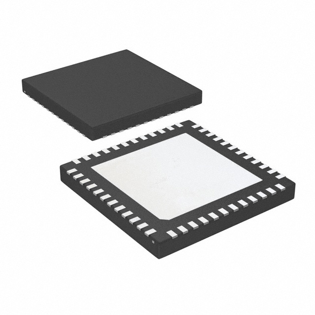
| 描述 | IC CLOCK CONDITIONER PLL 48-LLP时钟合成器/抖动清除器 Precision Clock Distributor with Integrated PLL 48-WQFN -40 to 85 |
| 产品分类 | |
| 品牌 | Texas Instruments |
| 产品手册 | |
| 产品图片 |
|
| rohs | 符合RoHS无铅 / 符合限制有害物质指令(RoHS)规范要求 |
| 产品系列 | 时钟和计时器IC,时钟合成器/抖动清除器,Texas Instruments LMK02002ISQ/NOPB- |
| 数据手册 | |
| 产品型号 | LMK02002ISQ/NOPB |
| PLL | 是 |
| 产品种类 | 时钟合成器/抖动清除器 |
| 供应商器件封装 | 48-WQFN(7X7) |
| 其它名称 | LMK02002ISQ/NOPBDKR |
| 分频器/倍频器 | 是/无 |
| 包装 | Digi-Reel® |
| 商标 | Texas Instruments |
| 安装类型 | 表面贴装 |
| 安装风格 | SMD/SMT |
| 封装 | Reel |
| 封装/外壳 | 48-WFQFN 裸露焊盘 |
| 封装/箱体 | WQFN-48 |
| 工作温度 | -40°C ~ 85°C |
| 工厂包装数量 | 250 |
| 差分-输入:输出 | 是/是 |
| 最大工作温度 | + 85 C |
| 最大输入频率 | 800 MHz |
| 最大输出频率 | 800 MHz |
| 最小工作温度 | - 40 C |
| 标准包装 | 1 |
| 比率-输入:输出 | 2:4 |
| 电压-电源 | 3.15 V ~ 3.45 V |
| 电源电压-最大 | 3.45 V |
| 电源电压-最小 | 3.15 V |
| 电源电流 | 70 mA |
| 电路数 | 1 |
| 类型 | 时钟调节器 |
| 系列 | LMK02002 |
| 输入 | LVCMOS,LVDS,LVPECL |
| 输入电平 | LVPECL, LVDS, LVCMOS |
| 输出 | LVPECL |
| 输出电平 | LVPECL |
| 输出端数量 | 4 Output |
| 频率-最大值 | 800MHz |


- 商务部:美国ITC正式对集成电路等产品启动337调查
- 曝三星4nm工艺存在良率问题 高通将骁龙8 Gen1或转产台积电
- 太阳诱电将投资9.5亿元在常州建新厂生产MLCC 预计2023年完工
- 英特尔发布欧洲新工厂建设计划 深化IDM 2.0 战略
- 台积电先进制程称霸业界 有大客户加持明年业绩稳了
- 达到5530亿美元!SIA预计今年全球半导体销售额将创下新高
- 英特尔拟将自动驾驶子公司Mobileye上市 估值或超500亿美元
- 三星加码芯片和SET,合并消费电子和移动部门,撤换高东真等 CEO
- 三星电子宣布重大人事变动 还合并消费电子和移动部门
- 海关总署:前11个月进口集成电路产品价值2.52万亿元 增长14.8%


PDF Datasheet 数据手册内容提取
LMK02002 www.ti.com SNAS418–AUGUST2007 LMK02002 Precision Clock Conditioner with Integrated PLL CheckforSamples:LMK02002 FEATURES DESCRIPTION 1 • 20fsAdditiveJitter The LMK02002 precision clock conditioner combines 2 the functions of jitter cleaning/reconditioning, • IntegratedInteger-NPLLwithOutstanding multiplication, and distribution of a reference clock. NormalizedPhaseNoiseContributionof-224 The device integrates a high performance Integer-N dBc/Hz Phase Locked Loop (PLL), and four LVPECL clock • ClockOutputFrequencyRangeof1to800 outputdistributionblocks. MHz Each clock distribution block includes a • 4LVPECLClockOutputs programmable divider, a phase synchronization • DedicatedDividerandDelayBlocksonEach circuit, a programmable delay, a clock output mux, and an LVPECL output buffer. This allows multiple ClockOutput integer-related and phase-adjusted copies of the • PinCompatibleFamilyofClockingDevices reference to be distributed to eight system • 3.15to3.45VOperation components. • Package:48PinWQFN(7.0x7.0x0.8mm) The clock conditioner comes in a 48-pin WQFN package and is footprint compatible with other TARGET APPLICATIONS clockingdevicesinthesamefamily. • DataConverterClocking • Networking,SONET/SDH,DSLAM • WirelessInfrastructure • Medical • TestandMeasurement • Military/Aerospace Functional Block Diagram OSCin R Divider OSCin* Phase Charge CPout Detector Pump N Divider Fin Fin* Distribution Path CLKout0 Divider Mux CLK Delay CLKout0* DATA PWire Control Port Registers LE CLKout1 Divider Mux CLKout1* Delay CLKout2 Divider Mux CLKout2* Delay GOE LD Device SYNC* Control CLKout3 Divider Mux CLKout3* Delay Clock Buffers 1 Pleasebeawarethatanimportantnoticeconcerningavailability,standardwarranty,anduseincriticalapplicationsof TexasInstrumentssemiconductorproductsanddisclaimerstheretoappearsattheendofthisdatasheet. Alltrademarksarethepropertyoftheirrespectiveowners. 2 PRODUCTIONDATAinformationiscurrentasofpublicationdate. Copyright©2007,TexasInstrumentsIncorporated Products conform to specifications per the terms of the Texas Instruments standard warranty. Production processing does not necessarilyincludetestingofallparameters.
LMK02002 SNAS418–AUGUST2007 www.ti.com Connection Diagram Figure1. 48-PinWQFNPackage 3* 3 2* 2 1* 1 0* 0 LKout LKout cc14 LKout LKout cc13 LKout LKout cc12 LKout LKout cc11 C C V C C V C C V C C V 48 47 46 45 44 43 42 41 40 39 38 37 GND 1 36 Bias NC 2 35 Fin* Vcc1 3 34 Fin CLKuWire 4 33 Vcc10 DATAuWire 5 32 CPout WQFN-48 LEuWire 6 31 Vcc9 Top Down View NC 7 30 Vcc8 Vcc2 8 29 OSCin* LDObyp1 9 28 OSCin LDObyp2 10 27 SYNC* DAP GOE 11 26 Vcc7 LD 12 25 GND 13 14 15 16 17 18 19 20 21 22 23 24 3 C C 4 C C 5 C C 6 C C cc N N cc N N cc N N cc N N V V V V PinDescriptions Pin# PinName I/O Description 1,25 GND - Ground 2,7,14,15,17,18,20, NC - NoConnectiontothesepins 21,23,24 3,8,13,16,19,22,26, Vcc1,Vcc2,Vcc3,Vcc4,Vcc5,Vcc6,Vcc7,Vcc8, - PowerSupply 30,31,33,37,40,43,46 Vcc9,Vcc10,Vcc11,Vcc12,Vcc13,Vcc14 4 CLKuWire I MICROWIREClockInput 5 DATAuWire I MICROWIREDataInput 6 LEuWire I MICROWIRELatchEnableInput 9,10 LDObyp1,LDObyp2 - LDOBypass 11 GOE I GlobalOutputEnable 12 LD O LockDetectandTestOutput 27 SYNC* I GlobalClockOutputSynchronization 28,29 OSCin,OSCin* I OscillatorClockInput;MustbeACcoupled 32 CPout O ChargePumpOutput 34,35 Fin,Fin* I FrequencyInput;MustbeACcoupled 36 Bias I BiasBypass 38,39 CLKout0,CLKout0* O LVPECLClockOutput0 41,42 CLKout1,CLKout1* O LVPECLClockOutput1 2 SubmitDocumentationFeedback Copyright©2007,TexasInstrumentsIncorporated ProductFolderLinks:LMK02002
LMK02002 www.ti.com SNAS418–AUGUST2007 PinDescriptions (continued) Pin# PinName I/O Description 44,45 CLKout2,CLKout2* O LVPECLClockOutput2 47,48 CLKout3,CLKout3* O LVPECLClockOutput3 DAP DAP - DieAttachPadisGround Thesedeviceshavelimitedbuilt-inESDprotection.Theleadsshouldbeshortedtogetherorthedeviceplacedinconductivefoam duringstorageorhandlingtopreventelectrostaticdamagetotheMOSgates. Absolute Maximum Ratings (1)(2)(3) Parameter Symbol Ratings Units PowerSupplyVoltage V -0.3to3.6 V CC InputVoltage V -0.3to(V +0.3) V IN CC StorageTemperatureRange T -65to150 °C STG LeadTemperature(solder4s) T +260 °C L JunctionTemperature T 125 °C J (1) "AbsoluteMaximumRatings"indicatelimitsbeyondwhichdamagetothedevicemayoccur,includinginoperabilityanddegradationof devicereliabilityand/orperformance.Functionaloperationofthedeviceand/ornon-degradationattheAbsoluteMaximumRatingsor otherconditionsbeyondthoseindicatedintheRecommendedOperatingConditionsisnotimplied.TheRecommendedOperating Conditionsindicateconditionsatwhichthedeviceisfunctionalandthedeviceshouldnotbeoperatedbeyondsuchconditions. (2) ThisdeviceisahighperformanceintegratedcircuitwithESDhandlingprecautions.HandlingofthisdeviceshouldonlybedoneatESD protectedworkstations.ThedeviceisratedtoaHBM-ESDof>2kV,aMM-ESDof>200V,andaCDM-ESDof>1.2kV. (3) IfMilitary/Aerospacespecifieddevicesarerequired,pleasecontacttheTISalesOffice/Distributorsforavailabilityandspecifications. Recommended Operating Conditions Parameter Symbol Min Typ Max Units AmbientTemperature T -40 25 85 °C A PowerSupplyVoltage V 3.15 3.3 3.45 V CC Package Thermal Resistance Package θ θ JA J-PAD(ThermalPad) 48-LeadWQFN (1) 27.4°C/W 5.8°C/W (1) Specificationassumes16thermalviasconnectthedieattachpadtotheembeddedcopperplaneonthe4-layerJEDECboard.These viasplayakeyroleinimprovingthethermalperformanceoftheWQFN.Itisrecommendedthatthemaximumnumberofviasbeusedin theboardlayout. Copyright©2007,TexasInstrumentsIncorporated SubmitDocumentationFeedback 3 ProductFolderLinks:LMK02002
LMK02002 SNAS418–AUGUST2007 www.ti.com Electrical Characteristics (1) (3.15V≤Vcc≤3.45V,-40°C≤T ≤85°C,DifferentialInputs/Outputs;exceptasspecified.Typicalvaluesrepresentmost A likelyparametricnormsatVcc=3.3V,T =25°C,andattheRecommendedOperationConditionsatthetimeofproduct A characterizationandarenotspecified). Symbol Parameter Conditions Min Typ Max Units CurrentConsumption Entiredevice;CLKout0&CLKout3 159 enabledinBypassMode I PowerSupplyCurrent (2) mA CC Entiredevice;AllOutputsOff(no 70 emitterresistorsplaced) I PD PowerDownCurrent POWERDOWN=1 1 mA CC ReferenceOscillator ReferenceOscillatorInputFrequency f square 1 200 MHz OSCin RangeforSquareWave ACcoupled;Differential(V ) OD SquareWaveInputVoltageforOSCinand V square 0.2 1.6 Vpp OSCin OSCin* FrequencyInput f FrequencyInputFrequencyRange 1 800 MHz Fin SLEW FrequencyInputSlewRate See (3)(4) 0.5 V/ns Fin DUTY FrequencyInputDutyCycle 40 60 % Fin P InputPowerRangeforFinorFin* ACcoupled -13 8 dBm Fin PLL f PhaseDetectorFrequency 40 MHz COMP V =Vcc/2,PLL_CP_GAIN=1x 100 CPout V =Vcc/2,PLL_CP_GAIN=4x 400 CPout I CPout ChargePumpSourceCurrent µA SRCE V =Vcc/2,PLL_CP_GAIN=16x 1600 CPout V =Vcc/2,PLL_CP_GAIN=32x 3200 CPout V =Vcc/2,PLL_CP_GAIN=1x -100 CPout V =Vcc/2,PLL_CP_GAIN=4x -400 CPout I CPout ChargePumpSinkCurrent μA SINK V =Vcc/2,PLL_CP_GAIN=16x -1600 CPout V =Vcc/2,PLL_CP_GAIN=32x -3200 CPout I TRI ChargePumpTRI-STATECurrent 0.5V<V <Vcc-0.5V 2 10 nA CPout CPout MagnitudeofChargePump V =Vcc/2 I %MIS CPout 3 % CPout Sinkvs.SourceCurrentMismatch T =25°C A MagnitudeofChargePump 0.5V<V <Vcc-0.5V I VTUNE CPout 4 % CPout Currentvs.ChargePumpVoltageVariation T =25°C A MagnitudeofChargePumpCurrentvs. I TEMP 4 % CPout TemperatureVariation PLL1/fNoiseat10kHzOffset (5) PLL_CP_GAIN=1x -117 PN10kHz dBc/Hz Normalizedto1GHzOutputFrequency PLL_CP_GAIN=32x -122 (1) TheElectricalCharacteristicstableslistensuredspecificationsunderthelistedRecommendedOperatingConditionsexceptas otherwisemodifiedorspecifiedbytheElectricalCharacteristicsConditionsand/orNotes.Typicalspecificationsareestimationsonlyand arenotensured. (2) SeeCURRENTCONSUMPTION/POWERDISSIPATIONCALCULATIONSformorecurrentconsumption/powerdissipation calculationinformation. (3) Forallfrequenciestheslewrate,SLEW ,ismeasuredbetween20%and80%. Fin (4) Specificationisensuredbycharacterizationandisnottestedinproduction. (5) AspecificationinmodelingPLLin-bandphasenoiseisthe1/fflickernoise,L (f),whichisdominantclosetothecarrier.Flicker PLL_flicker noisehasa10dB/decadeslope.PN10kHzisnormalizedtoa10kHzoffsetanda1GHzcarrierfrequency.PN10kHz=L (10 PLL_flicker kHz)-20log(Fout/1GHz),whereL (f)isthesinglesidebandphasenoiseofonlytheflickernoise'scontributiontototalnoise, PLL_flicker L(f).TomeasureL (f)itisimportanttobeonthe10dB/decadeslopeclosetothecarrier.Ahighphasedetectorfrequencyanda PLL_flicker cleancrystalareimportanttoisolatingthisnoisesourcefromthetotalphasenoise,L(f).L (f)canbemaskedbythereference PLL_flicker oscillatorperformanceifalowpowerornoisysourceisused.ThetotalPLLinbandphasenoiseperformanceisthesumofL (f) PLL_flicker andL (f). PLL_flat 4 SubmitDocumentationFeedback Copyright©2007,TexasInstrumentsIncorporated ProductFolderLinks:LMK02002
LMK02002 www.ti.com SNAS418–AUGUST2007 Electrical Characteristics (1) (continued) (3.15V≤Vcc≤3.45V,-40°C≤T ≤85°C,DifferentialInputs/Outputs;exceptasspecified.Typicalvaluesrepresentmost A likelyparametricnormsatVcc=3.3V,T =25°C,andattheRecommendedOperationConditionsatthetimeofproduct A characterizationandarenotspecified). Symbol Parameter Conditions Min Typ Max Units PLL_CP_GAIN=1x -219 PN1Hz NormalizedPhaseNoiseContribution(6) dBc/Hz PLL_CP_GAIN=32x -224 ClockDistributionSection (7)-LVPECLClockOutputs(CLKout0toCLKout3) CLKoutX_MUX= RL=100Ω Bypass 20 DistributionPath= Jitter AdditiveRMSJitter (7) 800MHz CLKoutX_MUX= fs ADD Bandwidth= Divided 75 12kHzto20MHz CLKoutX_DIV= 4 Equalloadingandidenticalclock t CLKoutXtoCLKoutY (4) configuration -30 ±3 30 ps SKEW Termination=50ΩtoVcc-2V Vcc- V OutputHighVoltage V OH 0.98 Termination=50ΩtoVcc-2V Vcc- V OutputLowVoltage CLKoutXoutputfrequency=200MHz V OL 1.8 V DifferentialOutputVoltage 660 810 965 mV OD DigitalLVTTLInterfaces (8) V High-LevelInputVoltage 2.0 Vcc V IH V Low-LevelInputVoltage 0.8 V IL I High-LevelInputCurrent V =Vcc -5.0 5.0 µA IH IH I Low-LevelInputCurrent V =0 -40.0 5.0 µA IL IL Vcc- V High-LevelOutputVoltage I =+500µA V OH OH 0.4 V Low-LevelOutputVoltage I =-500µA 0.4 V OL OL DigitalMICROWIREInterfaces (9) V High-LevelInputVoltage 1.6 Vcc V IH V Low-LevelInputVoltage 0.4 V IL I High-LevelInputCurrent V =Vcc -5.0 5.0 µA IH IH I Low-LevelInputCurrent V =0 -5.0 5.0 µA IL IL MICROWIRETiming t DatatoClockSetUpTime SeeDataInputTiming 25 ns CS t DatatoClockHoldTime SeeDataInputTiming 8 ns CH t ClockPulseWidthHigh SeeDataInputTiming 25 ns CWH t ClockPulseWidthLow SeeDataInputTiming 25 ns CWL t ClocktoEnableSetUpTime SeeDataInputTiming 25 ns ES t EnabletoClockSetUpTime SeeDataInputTiming 25 ns CES t EnablePulseWidthHigh SeeDataInputTiming 25 ns EWH (6) AspecificationinmodelingPLLin-bandphasenoiseistheNormalizedPhaseNoiseContribution,L (f),ofthePLLandisdefined PLL_flat asPN1Hz=L (f)–20log(N)–10log(f ).L (f)isthesinglesidebandphasenoisemeasuredatanoffsetfrequency,f,ina PLL_flat COMP PLL_flat 1HzBandwidthandf isthephasedetectorfrequencyofthesynthesizer.L (f)contributestothetotalnoise,L(f).Tomeasure COMP PLL_flat L (f)theoffsetfrequency,f,mustbechosensufficientlysmallerthentheloopbandwidthofthePLL,andyetlargeenoughtoavoid PLL_flat asubstantialnoisecontributionfromthereferenceandflickernoise.L (f)canbemaskedbythereferenceoscillatorperformanceif PLL_flat alowpowerornoisysourceisused. (7) TheClockDistributionSectionincludesallpartsofthedeviceexceptthePLLsection.TypicalAdditiveJitterspecificationsapplytothe clockdistributionsectiononly. (8) AppliestoGOE,LD,andSYNC*. (9) AppliestoCLKuWire,DATAuWire,andLEuWire. Copyright©2007,TexasInstrumentsIncorporated SubmitDocumentationFeedback 5 ProductFolderLinks:LMK02002
LMK02002 SNAS418–AUGUST2007 www.ti.com Serial Data Timing Diagram MSB LSB DATAuWire D27 D26 D25 D24 D23 D0 A3 A2 A1 A0 CLKuWire tCES tCS tCH tCWH tCWL tES LEuWire tEWH Data bits set on the DATAuWire signal are clocked into a shift register, MSB first, on each rising edge of the CLKuWire signal. On the rising edge of the LEuWire signal, the data is sent from the shift register to the addressed register determined by the LSB bits. After the programming is complete the CLKuWire, DATAuWire, andLEuWiresignalsshouldbereturnedtoalowstate. Charge Pump Current Specification Definitions I1=ChargePumpSinkCurrentatV =Vcc-ΔV CPout I2=ChargePumpSinkCurrentatV =Vcc/2 CPout I3=ChargePumpSinkCurrentatV =ΔV CPout I4=ChargePumpSourceCurrentatV =Vcc-ΔV CPout I5=ChargePumpSourceCurrentatV =Vcc/2 CPout I6=ChargePumpSourceCurrentatV =ΔV CPout ΔV=Voltageoffsetfromthepositiveandnegativesupplyrails.Definedtobe0.5Vforthisdevice. ChargePumpOutputCurrentMagnitudeVariationvs.ChargePumpOutputVoltage 6 SubmitDocumentationFeedback Copyright©2007,TexasInstrumentsIncorporated ProductFolderLinks:LMK02002
LMK02002 www.ti.com SNAS418–AUGUST2007 Charge Pump Current Specification Definitions (continued) ChargePumpSinkCurrentvs.ChargePumpOutputSourceCurrentMismatch ChargePumpOutputCurrentMagnitudeVariationvs.Temperature Functional Description The LMK02002 precision clock conditioner combines the functions of jitter cleaning/reconditioning, multiplication, and distribution of a reference clock. The device integrates a high performance Integer-N Phase Locked Loop (PLL),andfourLVPECLclockoutputdistributionblocks. Each clock distribution block includes a programmable divider, a phase synchronization circuit, a programmable delay, a clock output mux, and an LVPECL output buffer. This allows multiple integer-related and phase-adjusted copiesofthereferencetobedistributedtoeightsystemcomponents. The clock conditioner comes in a 48-pin WQFN package and is footprint compatible with other clocking devices inthesamefamily. BIAS PIN To properly use the device, bypass Bias (pin 36) with a low leakage 1 µF capacitor connected to Vcc. This is importantforlownoiseperformance. LDO BYPASS To properly use the device, bypass LDObyp1 (pin 9) with a 10 µF capacitor and LDObyp2 (pin 10) with a 0.1 µF capacitor. OSCILLATOR INPUT PORT (OSCin, OSCin*) The purpose of OSCin is to provide the PLL with a reference signal. The OSCin port must be AC coupled, refer to the System Level Diagram in the Application Information section. The OSCin port may be driven single endedlybyACgroundingOSCin*witha0.1µFcapacitor. FREQUENCY INPUT PORT (Fin, Fin*) The purpose of Fin is to provide the PLL with a feedback signal from an external oscillator. The Fin port may be drivensingleendedlybyACgroundingFin*. Copyright©2007,TexasInstrumentsIncorporated SubmitDocumentationFeedback 7 ProductFolderLinks:LMK02002
LMK02002 SNAS418–AUGUST2007 www.ti.com CLKout DELAYS Each individual clock output includes a delay adjustment. Clock output delay registers (CLKoutX_DLY) support a 150psstepsizeandrangefrom0to2250psoftotaldelay. LVPECL OUTPUTS Each LVPECL output may be disabled individually by programming the CLKoutX_EN bits. All the outputs may be disabledsimultaneouslybypullingtheGOEpinloworprogrammingEN_CLKout_Globalto0. GLOBAL CLOCK OUTPUT SYNCHRONIZATION The SYNC* pin synchronizes the clock outputs. When the SYNC* pin is held in a logic low state, the divided outputs are also held in a logic low state. When the SYNC* pin goes high, the divided clock outputs are activated and will transition to a high state simultaneously. Clocks in the bypassed state are not affected by SYNC* and arealwayssynchronizedwiththedividedoutputs. The SYNC* pin must be held low for greater than one clock cycle of the Frequency Input port, also known as the distribution path. Once this low event has been registered, the outputs will not reflect the low state for four more cycles. Similarly once the SYNC* pin becomes high, the outputs will not simultaneously transition high until four more distribution path clock cycles have passed. See the timing diagram below for further detail. In the timing diagram below the clocks are programmed as CLKout0_MUX = Bypassed, CLKout1_MUX = Divided, CLKout1_DIV=2,CLKout2_MUX=Divided,andCLKout2_DIV=4. SYNC* Timing Diagram Distribution Path SYNC* CLKout0 CLKout1 CLKout2 The SYNC* pin provides an internal pull-up resistor as shown on the functional block diagram. If the SYNC* pin is not terminated externally the clock outputs will operate normally. If the SYNC* function is not used, clock outputsynchronizationisnotspecified. CLKout OUTPUT STATES Each clock output may be individually enabled with the CLKoutX_EN bits. Each individual output enable control bit is gated with the Global Output Enable input pin (GOE) and the Global Output Enable bit (EN_CLKout_Global). All clock outputs can be disabled simultaneously if the GOE pin is pulled low by an external signal or EN_CLKout_Globalissetto0. CLKoutX EN_CLKout GOEpin ClockXOutputState _ENbit _Globalbit 1 1 Low Low Don'tcare 0 Don'tcare Off 0 Don'tcare Don'tcare Off 1 1 High/NoConnect Enabled 8 SubmitDocumentationFeedback Copyright©2007,TexasInstrumentsIncorporated ProductFolderLinks:LMK02002
LMK02002 www.ti.com SNAS418–AUGUST2007 WhenanLVPECLoutputisintheOffstate,theoutputsareatavoltageofapproximately1volt. GLOBAL OUTPUT ENABLE AND LOCK DETECT The GOE pin provides an internal pull-up resistor. If it is not terminated externally, the clock output states are determinedbytheClockOutputEnablebits(CLKoutX_EN)andtheEN_CLKout_Globalbit. By programming the PLL_MUX register to Digital Lock Detect Active High (See PLL_MUX[3:0] -- Multiplexer Control for LD Pin), the Lock Detect (LD) pin can be connected to the GOE pin in which case all outputs are set lowautomaticallyifthesynthesizerisnotlocked. POWER ON RESET When supply voltage to the device increases monotonically from ground to Vcc, the power on reset circuit sets all registers to their default values, see RESET bit -- R0 only for more information on default register values. VoltageshouldbeappliedtoallVccpinssimultaneously. General Programming Information The LMK02002 device is programmed using several 32-bit registers which control the device's operation. The registers consist of a data field and an address field. The last 4 register bits, ADDR[3:0] form the address field. Theremaining28bitsformthedatafieldDATA[27:0]. During programming, LEuWire is low and serial data is clocked in on the rising edge of clock (MSB first). When LEuWire goes high, data is transferred to the register bank selected by the address field. Only registers R0 to R7,R11,R14,andR15needtobeprogrammedforproperdeviceoperation. ItisrequiredtoprogramregisterR14. RECOMMENDEDPROGRAMMINGSEQUENCE The recommended programming sequence involves programming R0 with the reset bit set (RESET = 1) to ensure the device is in a default state. It is not necessary to program R0 again. Registers are programmed in orderwithR15beingthelastregisterprogrammed.Anexampleprogrammingsequenceisshownbelow. • ProgramR0withtheresetbitset(RESET=1).Thisensuresthedeviceisinadefaultstate. • ProgramR4toR7asnecessarywithdesiredclockswithappropriateenable,mux,divider,anddelaysettings. • ProgramR11withDIV4settingifnecessary. • Program R14 with global clock output bit, power down setting, PLL mux setting, and PLL R divider. It is requiredtoprogramregisterR14. – R14 must be programmed in accordance with the register map as shown in the register map (see Table1). • ProgramR15withPLLchargepumpgain,andPLLNdivider. Copyright©2007,TexasInstrumentsIncorporated SubmitDocumentationFeedback 9 ProductFolderLinks:LMK02002
LMK02002 SNAS418–AUGUST2007 www.ti.com Table1.LMK02002REGISTERMAP Re gist 31 30 29 28 27 26 25 24 23 22 21 20 19 18 17 16 15 14 13 12 11 10 9 8 7 6 5 4 3 2 1 0 er Data[27:0] A3 A2 A1 A0 RE R0 SE 0 0 0 0 0 0 0 0 0 0 0 0 0 0 0 0 0 0 0 0 0 0 0 0 0 0 0 0 0 0 0 T CL CLKout0 Kou CLKout0_DIV CLKout0_DLY R4 0 0 0 0 0 0 0 0 0 0 0 0 0 _MUX 0 1 0 0 t0_ [7:0] [3:0] [1:0] EN CL CLKout1 Kou CLKout1_DIV CLKout1_DLY R5 0 0 0 0 0 0 0 0 0 0 0 0 0 _MUX 0 1 0 1 t1_ [7:0] [3:0] [1:0] EN CL CLKout2 Kou CLKout2_DIV CLKout2_DLY R6 0 0 0 0 0 0 0 0 0 0 0 0 0 _MUX 0 1 1 0 t2_ [7:0] [3:0] [1:0] EN CL CLKout3 Kou CLKout3_DIV CLKout3_DLY R7 0 0 0 0 0 0 0 0 0 0 0 0 0 _MUX 0 1 1 1 t3_ [7:0] [3:0] [1:0] EN DIV R11 0 0 0 0 0 0 0 0 1 0 0 0 0 0 1 0 0 0 0 0 0 0 0 0 0 0 0 1 0 1 1 4 EN PO TRI PLL _CL WE - _C Kou PLL_MUX PLL_R R14 0 0 1 0 RD ST P_ 0 0 0 0 1 1 1 0 t_Gl [3:0] [11:0] OW AT PO oba N E L l PLL_ CP_ PLL_N R15 0 0 0 0 0 0 0 0 1 1 1 1 GAIN [17:0] [1:0] 10 SubmitDocumentationFeedback Copyright©2007,TexasInstrumentsIncorporated ProductFolderLinks:LMK02002
LMK02002 www.ti.com SNAS418–AUGUST2007 REGISTERR4toR7 Registers R4 through R7 control the eight clock outputs. Register R4 controls CLKout0, Register R5 controls CLKout1, and so on. There is one additional bit in register R0 called RESET. Aside from this, the functions of these bits are identical. The X in CLKoutX_MUX, CLKoutX_DIV, CLKoutX_DLY, and CLKoutX_EN denote the actualclockoutputwhichmaybefrom0to3. RESETbit--R0only This bit is only in register R0. The use of this bit is optional and it should be set to '0' if not used. Setting this bit to a '1' forces all registers to their power on reset condition and therefore automatically clears this bit. If this bit is set, all other R0 bits are ignored and R0 needs to be programmed again if used with its proper values and RESET=0. Default Bit BitName BitState BitDescription Register BitValue Location RESET 0 Noreset,normaloperation Resettopowerondefaults R0 31 CLKoutX_MUX 0 Bypassed CLKoutXmuxmode 18:17 CLKoutX_EN 0 Disabled CLKoutXenable 16 R4toR7 CLKoutX_DIV 1 Divideby2 CLKoutXclockdivide 15:8 CLKoutX_DLY 0 0ps CLKoutXclockdelay 7:4 DIV4 0 PDF≤20MHz PhaseDetectorFrequency R11 15 EN_CLKout_Global 1 Normal-CLKoutsnormal Globalclockoutputenable 27 POWERDOWN 0 Normal-Deviceactive Devicepowerdown 26 PLL_CP_TRI 0 Normal-PLLactive TRI-STATEPLLchargepump 25 R14 PLL_CP_POL 0 NegativePolarityCP Polarityofchargepump 24 PLL_MUX 0 Disabled MultiplexercontrolforLDpin 23:20 PLL_R 10 Rdivider=10 PLLRdividevalue 19:8 PLL_CP_GAIN 0 100uA Chargepumpcurrent 31:30 R15 PLL_N 760 Ndivider=760 PLLNdividevalue 25:8 CLKoutX_MUX[1:0]--ClockOutputMultiplexers These bits control the Clock Output Multiplexer for each clock output. Changing between the different modes changes the blocks in the signal path and therefore incurs a delay relative to the bypass mode. The different MUXmodesandassociateddelaysarelistedbelow. CLKoutX_MUX[1:0] Mode AddedDelayRelativetoBypassMode 0 Bypassed(default) 0ps 1 Divided 100ps 400ps 2 Delayed (Inadditiontotheprogrammeddelay) 500ps 3 DividedandDelayed (Inadditiontotheprogrammeddelay) CLKoutX_DIV[7:0]--ClockOutputDividers These bits control the clock output divider value. In order for these dividers to be active, the respective CLKoutX_MUX (See CLKoutX_MUX[1:0] -- Clock Output Multiplexers) bit must be set to either "Divided" or "DividedandDelayed"mode.Afterallthedividersareprogramed,theSYNC*pinmustbeusedtoensurethatall edges of the clock outputs are aligned (See GLOBAL CLOCK OUTPUT SYNCHRONIZATION). The Clock Output Dividers follow the VCO Divider so the final clock divide for an output is VCO Divider × Clock Output Divider.Byaddingthedividerblocktotheoutputpathafixeddelayofapproximately100psisincurred. TheactualClockOutputDividevalueistwicethebinaryvalueprogrammedaslistedinthetablebelow. Copyright©2007,TexasInstrumentsIncorporated SubmitDocumentationFeedback 11 ProductFolderLinks:LMK02002
LMK02002 SNAS418–AUGUST2007 www.ti.com CLKoutX_DIV[7:0] ClockOutputDividervalue 0 0 0 0 0 0 0 0 Invalid 0 0 0 0 0 0 0 1 2(default) 0 0 0 0 0 0 1 0 4 0 0 0 0 0 0 1 1 6 0 0 0 0 0 1 0 0 8 0 0 0 0 0 1 0 1 10 . . . . . . . . ... 1 1 1 1 1 1 1 1 510 CLKoutX_DLY[3:0]--ClockOutputDelays These bits control the delay stages for each clock output. In order for these delays to be active, the respective CLKoutX_MUX (See CLKoutX_MUX[1:0] -- Clock Output Multiplexers) bit must be set to either "Delayed" or "Divided and Delayed" mode. By adding the delay block to the output path a fixed delay of approximately 400 ps isincurredinadditiontothedelayshowninthetablebelow. CLKoutX_DLY[3:0] Delay(ps) 0 0(default) 1 150 2 300 3 450 4 600 5 750 6 900 7 1050 8 1200 9 1350 10 1500 11 1650 12 1800 13 1950 14 2100 15 2250 CLKoutX_ENbit--ClockOutputEnables These bits control whether an individual clock output is enabled or not. If the EN_CLKout_Global bit (See EN_CLKout_Global bit -- Global Clock Output Enable) is set to zero or if GOE pin is held low, all CLKoutX_EN bit states will be ignored and all clock outputs will be disabled. See CLKout OUTPUT STATES for more informationonCLKoutstates. CLKoutX_ENbit Conditions CLKoutXState 0 EN_CLKout_Globalbit=1 Disabled(default) GOEpin=High/NoConnect1 1 Enabled REGISTERR11 This register only has one bit and only needs to be programmed in the case that the phase detector frequency is greaterthan20MHzanddigitallockdetectisused.Otherwise,itisautomaticallydefaultedtothecorrectvalues. DIV4 This bit divides the frequency presented to the digital lock detect circuitry by 4. It is necessary to get a reliable outputfromthedigitallockdetectoutputinthecaseofaphasedetectorfrequencygreaterthan20MHz. 12 SubmitDocumentationFeedback Copyright©2007,TexasInstrumentsIncorporated ProductFolderLinks:LMK02002
LMK02002 www.ti.com SNAS418–AUGUST2007 DIV4 DigitalLockDetectCircuitryMode 0 Notdivided;Phasedetectorfrequency≤20MHz(default) 1 Dividedby4;Phasedetectorfrequency>20MHz REGISTERR14 TheLMK02002requiresregisterR14tobeprogrammedasshownintheregistermap(seeTable1). PLL_R[11:0]--RDividerValue ThesebitsprogramthePLLRDividerandareprogrammedinbinaryfashion. PLL_R[11:0] PLLRDivideValue 0 0 0 0 0 0 0 0 0 0 0 0 Invalid 0 0 0 0 0 0 0 0 0 0 0 1 1 0 0 0 0 0 0 0 0 0 0 1 0 2 . . . . . . . . . . . . ... 0 0 0 0 0 0 0 0 1 0 1 0 10(default) . . . . . . . . . . . . ... 1 1 1 1 1 1 1 1 1 1 1 1 4095 PLL_MUX[3:0]--MultiplexerControlforLDPin ThesebitssettheoutputmodeoftheLDpin.Thetablebelowlistsseveraldifferentmodes. PLL_MUX[3:0] OutputType LDPinFunction 0 Hi-Z Disabled(default) 1 Push-Pull LogicHigh 2 Push-Pull LogicLow 3 Push-Pull DigitalLockDetect(ActiveHigh) 4 Push-Pull DigitalLockDetect(ActiveLow) 5 Push-Pull AnalogLockDetect 6 OpenDrainNMOS AnalogLockDetect 7 OpenDrainPMOS AnalogLockDetect 8 Invalid 9 Push-Pull NDividerOutput/2(50%DutyCycle) 10 Invalid 11 Push-Pull RDividerOutput/2(50%DutyCycle) 12to15 Invalid POWERDOWNbit--DevicePowerDown This bit can power down the device. Enabling this bit powers down the entire device and all blocks, regardless of thestateofanyoftheotherbitsorpins. POWERDOWNbit Mode 0 NormalOperation(default) 1 EntireDevicePoweredDown EN_CLKout_Globalbit--GlobalClockOutputEnable This bit overrides the individual CLKoutX_EN bits (See CLKoutX_EN bit -- Clock Output Enables). When this bit is set to 0, all clock outputs are disabled, regardless of the state of any of the other bits or pins. See CLKout OUTPUTSTATESformoreinformationonCLKoutstates. Copyright©2007,TexasInstrumentsIncorporated SubmitDocumentationFeedback 13 ProductFolderLinks:LMK02002
LMK02002 SNAS418–AUGUST2007 www.ti.com EN_CLKout_Globalbit ClockOutputs 0 AllOff 1 NormalOperation(default) PLL_CP_TRIbit--PLLChargePumpTRI-STATE ThisbitsetsthePLLchargepumpTRI-STATE. PLL_CP_TRI PLLChargePump 0 Normaloperation(default) 1 TRI-STATE PLL_CP_POLbit--PLLChargePumpPolarity Thisbitsetsthepolarityofthechargepumptoeithernegativeorpositive.Anegativechargepumpisusedwitha VCO or VCXO which decreases frequency with increasing tuning voltage. A positive charge pump is used with a VCOorVCXOwhichincreasesfrequencywithincreasingtuningvoltage. PLL_CP_POL PLLChargePumpPolarity 0 Negative(default) 1 Positive RegisterR15 PLL_N[17:0]--PLLNDivider These bits program the divide value for the PLL N Divider. The PLL N Divider follows the VCO Divider and precedes the PLL phase detector. Since the VCO Divider is also in the feedback path from the VCO to the PLL Phase Detector, the total N divide value, N , is also influenced by the VCO Divider value. N = PLL N Total Total Divider×VCODivider.TheVCOfrequencyiscalculatedas,f =f ×PLLNDivider ×VCODivider/PLLR VCO OSCin Divider. Since the PLL N divider is a pure binary counter, there are no illegal divide values for PLL_N[17:0] exceptfor0. PLL_N[17:0] PLLNDividerValue 0 0 0 0 0 0 0 0 0 0 0 0 0 0 0 0 0 0 Invalid 0 0 0 0 0 0 0 0 0 0 0 0 0 0 0 0 0 1 1 . . . . . . . . . . . . . . . . . . ... 0 0 0 0 0 0 0 0 1 0 1 1 1 1 1 0 0 0 760(default) . . . . . . . . . . . . . . . . . . ... 1 1 1 1 1 1 1 1 1 1 1 1 1 1 1 1 1 1 262143 PLL_CP_GAIN[1:0]--PLLChargePumpGain ThesebitssetthechargepumpgainofthePLL. PLL_CP_GAIN[1:0] ChargePumpGain 0 1x(default) 1 4x 2 16x 3 32x 14 SubmitDocumentationFeedback Copyright©2007,TexasInstrumentsIncorporated ProductFolderLinks:LMK02002
LMK02002 www.ti.com SNAS418–AUGUST2007 APPLICATION INFORMATION SYSTEM LEVEL DIAGRAM The following shows the LMK02002 in a typical application. In this setup the clock may be multiplied, reconditioned,andredistributed. Vcc 100(cid:214) 0.1 PF 0.1 PF 1 PF ut CPo Fin Fin* Bias 0.1 PF OSCin CLKout0 100(cid:214) OSCin* CLKout0* CLKout1 0.1 PF CLKout1* CLKout2 To System CLKout2* LEuWire CLKuWire CLKout3 DATAuWire CLKout3* To Host SYNC* LMK02002 LD (optional) GOE LDObyp1 LDObyp2 10 PF 0.1 PF Figure2. TypicalApplication BIAS PIN To properly use the device, bypass Bias (pin 36) with a low leakage 1 µF capacitor connected to Vcc. This is importantforlownoiseperformance. LDO BYPASS To properly use the device, bypass LDObyp1 (pin 9) with a 10 µF capacitor and LDObyp2 (pin 10) with a 0.1 µF capacitor. CURRENT CONSUMPTION / POWER DISSIPATION CALCULATIONS Due to the myriad of possible configurations the following table serves to provide enough information to allow the user to calculate estimated current consumption of the LMK02002. Unless otherwise noted Vcc = 3.3 V, T = 25 A °C. Copyright©2007,TexasInstrumentsIncorporated SubmitDocumentationFeedback 15 ProductFolderLinks:LMK02002
LMK02002 SNAS418–AUGUST2007 www.ti.com Table2. BlockCurrentConsumption Power Current Power Dissipatedin Block Condition Consumptionat Dissipatedin LVPECLemitter 3.3V(mA) device(mW) resistors(mW) Entiredevice, Alloutputsoff;NoLVPECLemitterresistorsconnected 70 231 - corecurrent Clockbuffers ThelowclockbufferisenabledanytimeoneofCLKout0 9 29.7 - (internal) throughCLKout3areenabled LVPECLoutput,bypassmode(includes120Ωemitter 40 72 60 resistors) LVPECLoutput,disabledmode(includes120Ωemitter Outputbuffers 17.4 38.3 19.1 resistors) LVPECLoutput,disabledmode.Noemitterresistors 0 0 - placed;openoutputs Dividecircuitry Divideenabled,divide=2 5.3 17.5 - peroutput Divideenabled,divide>2 8.5 28.0 - Delaycircuitryper Delayenabled,delay<8 5.8 19.1 - output Delayenabled,delay>7 9.9 32.7 - Entiredevice CLKout0&CLKout3enabledinbypassmode 159 404.7 120 From Table 2 the current consumption can be calculated in any configuration. For example, the current for the entire device with two LVPECL (CLKout0 and CLKout3) outputs in bypass mode can be calculated by adding up the following blocks: core current, clock buffers, and two LVPECL output buffer currents. There will also be two LVPECL outputs drawing emitter current, but some of the power from the current draw is dissipated in the external120Ω resistorswhichdoesn'taddtothepowerdissipationbudgetforthedevice.Ifdelaysordividesare switchedin,thentheadditionalcurrentforthesestagesneedstobeaddedaswell. For power dissipated by the device, the total current entering the device is multiplied by the voltage at the device minus the power dissipated in any emitter resistors connected to any of the LVPECL outputs. If no emitter resistors are connected to the LVPECL outputs, this power will be 0 watts. For example, in the case of two LVPECL (CLKout0 and CLKout3) operating at 3.3 volts, we calculate 3.3 V × (70 + 9 + 40 + 40) mA = 3.3 V × 159 mA = 524.7 mW. Because the LVPECL outputs have emitter resistors hooked up and the power dissipated by these resistors is 60 mW for each clock, the total device power dissipation is 524.7 mW - 120 mW = 404.7 mW. When an LVPECL output is active, ~1.9 V is the average voltage on each output as calculated from the LVPECL V &V typicalspecification.Thereforethepowerdissipatedineachemitterresistorisapproximately(1.9V)2/ OH OL 120 Ω = 30 mW. When an LVPECL output is disabled, the emitter resistor voltage is ~1.07 V. Therefore the powerdissipatedineachemitterresistorisapproximately(1.07V)2/120Ω =9.5mW. THERMAL MANAGEMENT Power consumption of the LMK02002 can be high enough to require attention to thermal management. For reliabilityandperformancereasonsthedietemperatureshouldbelimitedtoamaximumof125°C.Thatis,asan estimate,T (ambienttemperature)plusdevicepowerconsumptiontimesθ shouldnotexceed125 °C. A JA The package of the device has an exposed pad that provides the primary heat removal path as well as excellent electrical grounding to the printed circuit board. To maximize the removal of heat from the package a thermal land pattern including multiple vias to a ground plane must be incorporated on the PCB within the footprint of the package. The exposed pad must be soldered down to ensure adequate heat conduction out of the package. A recommended land and via pattern is shown in Figure 3. More information on soldering WQFN packages can be obtainedatwww.ti.com. 16 SubmitDocumentationFeedback Copyright©2007,TexasInstrumentsIncorporated ProductFolderLinks:LMK02002
LMK02002 www.ti.com SNAS418–AUGUST2007 5.0 mm, min 0.33 mm, typ 1.2 mm, typ Figure3. To minimize junction temperature it is recommended that a simple heat sink be built into the PCB (if the ground plane layer is not exposed). This is done by including a copper area of about 2 square inches on the opposite side of the PCB from the device. This copper area may be plated or solder coated to prevent corrosion but should not have conformal coating (if possible), which could provide thermal insulation. The vias shown in Figure 3 should connect these top and bottom copper layers and to the ground layer. These vias act as “heat pipes” to carry the thermal energy away from the device side of the board to where it can be more effectively dissipated. Copyright©2007,TexasInstrumentsIncorporated SubmitDocumentationFeedback 17 ProductFolderLinks:LMK02002
PACKAGE OPTION ADDENDUM www.ti.com 6-Feb-2020 PACKAGING INFORMATION Orderable Device Status Package Type Package Pins Package Eco Plan Lead/Ball Finish MSL Peak Temp Op Temp (°C) Device Marking Samples (1) Drawing Qty (2) (6) (3) (4/5) LMK02002ISQ/NOPB ACTIVE WQFN RHS 48 250 Green (RoHS SN Level-3-260C-168 HR -40 to 85 K02002 I & no Sb/Br) LMK02002ISQX/NOPB ACTIVE WQFN RHS 48 2500 Green (RoHS SN Level-3-260C-168 HR -40 to 85 K02002 I & no Sb/Br) (1) The marketing status values are defined as follows: ACTIVE: Product device recommended for new designs. LIFEBUY: TI has announced that the device will be discontinued, and a lifetime-buy period is in effect. NRND: Not recommended for new designs. Device is in production to support existing customers, but TI does not recommend using this part in a new design. PREVIEW: Device has been announced but is not in production. Samples may or may not be available. OBSOLETE: TI has discontinued the production of the device. (2) RoHS: TI defines "RoHS" to mean semiconductor products that are compliant with the current EU RoHS requirements for all 10 RoHS substances, including the requirement that RoHS substance do not exceed 0.1% by weight in homogeneous materials. Where designed to be soldered at high temperatures, "RoHS" products are suitable for use in specified lead-free processes. TI may reference these types of products as "Pb-Free". RoHS Exempt: TI defines "RoHS Exempt" to mean products that contain lead but are compliant with EU RoHS pursuant to a specific EU RoHS exemption. Green: TI defines "Green" to mean the content of Chlorine (Cl) and Bromine (Br) based flame retardants meet JS709B low halogen requirements of <=1000ppm threshold. Antimony trioxide based flame retardants must also meet the <=1000ppm threshold requirement. (3) MSL, Peak Temp. - The Moisture Sensitivity Level rating according to the JEDEC industry standard classifications, and peak solder temperature. (4) There may be additional marking, which relates to the logo, the lot trace code information, or the environmental category on the device. (5) Multiple Device Markings will be inside parentheses. Only one Device Marking contained in parentheses and separated by a "~" will appear on a device. If a line is indented then it is a continuation of the previous line and the two combined represent the entire Device Marking for that device. (6) Lead/Ball Finish - Orderable Devices may have multiple material finish options. Finish options are separated by a vertical ruled line. Lead/Ball Finish values may wrap to two lines if the finish value exceeds the maximum column width. Important Information and Disclaimer:The information provided on this page represents TI's knowledge and belief as of the date that it is provided. TI bases its knowledge and belief on information provided by third parties, and makes no representation or warranty as to the accuracy of such information. Efforts are underway to better integrate information from third parties. TI has taken and continues to take reasonable steps to provide representative and accurate information but may not have conducted destructive testing or chemical analysis on incoming materials and chemicals. TI and TI suppliers consider certain information to be proprietary, and thus CAS numbers and other limited information may not be available for release. In no event shall TI's liability arising out of such information exceed the total purchase price of the TI part(s) at issue in this document sold by TI to Customer on an annual basis. Addendum-Page 1
PACKAGE OPTION ADDENDUM www.ti.com 6-Feb-2020 Addendum-Page 2
PACKAGE MATERIALS INFORMATION www.ti.com 20-Sep-2016 TAPE AND REEL INFORMATION *Alldimensionsarenominal Device Package Package Pins SPQ Reel Reel A0 B0 K0 P1 W Pin1 Type Drawing Diameter Width (mm) (mm) (mm) (mm) (mm) Quadrant (mm) W1(mm) LMK02002ISQ/NOPB WQFN RHS 48 250 178.0 16.4 7.3 7.3 1.3 12.0 16.0 Q1 LMK02002ISQX/NOPB WQFN RHS 48 2500 330.0 16.4 7.3 7.3 1.3 12.0 16.0 Q1 PackMaterials-Page1
PACKAGE MATERIALS INFORMATION www.ti.com 20-Sep-2016 *Alldimensionsarenominal Device PackageType PackageDrawing Pins SPQ Length(mm) Width(mm) Height(mm) LMK02002ISQ/NOPB WQFN RHS 48 250 210.0 185.0 35.0 LMK02002ISQX/NOPB WQFN RHS 48 2500 367.0 367.0 38.0 PackMaterials-Page2
PACKAGE OUTLINE RHS0048A WQFN - 0.8 mm max height SCALE 1.800 PLASTIC QUAD FLATPACK - NO LEAD A 7.15 B 6.85 PIN 1 INDEX AREA 0.5 0.3 7.15 6.85 0.30 0.18 DETAIL OPTIONAL TERMINAL TYPICAL 0.8 0.7 C DIM A SEATING PLANE OPT 1 OPT 2 0.05 0.08 C (0.1) (0.2) 0.00 2X 5.5 (0.2) 5.1 0.1 (A) TYP 44X 0.5 13 24 12 25 EXPOSED THERMAL PAD 2X 49 SYMM 5.5 SEE TERMINAL DETAIL 1 36 0.30 48X 48 37 0.18 PIN 1 ID SYMM 0.5 0.1 C A B (OPTIONAL) 48X 0.3 0.05 4214990/B 04/2018 NOTES: 1. All linear dimensions are in millimeters. Any dimensions in parenthesis are for reference only. Dimensioning and tolerancing per ASME Y14.5M. 2. This drawing is subject to change without notice. 3. The package thermal pad must be soldered to the printed circuit board for thermal and mechanical performance. www.ti.com
EXAMPLE BOARD LAYOUT RHS0048A WQFN - 0.8 mm max height PLASTIC QUAD FLATPACK - NO LEAD ( 5.1) SYMM 48 37 48X (0.6) 1 36 48X (0.25) (1.05) TYP 44X (0.5) (1.25) TYP 49 SYMM (6.8) (R0.05) TYP ( 0.2) TYP VIA 12 25 13 24 (1.25) (1.05) TYP TYP (6.8) LAND PATTERN EXAMPLE EXPOSED METAL SHOWN SCALE:12X 0.07 MAX 0.07 MIN ALL AROUND ALL AROUND SOLDER MASK METAL EDGE OPENING EXPOSED METAL SOLDER MASK EXPOSED METAL UNDER OPENING METAL SOLDER MASK NON SOLDER MASK SOLDER MASK DEFINED DEFINED (PREFERRED) SOLDER MASK DETAILS 4214990/B 04/2018 NOTES: (continued) 4. This package is designed to be soldered to a thermal pad on the board. For more information, see Texas Instruments literature number SLUA271 (www.ti.com/lit/slua271). 5. Vias are optional depending on application, refer to device data sheet. If any vias are implemented, refer to their locations shown on this view. It is recommended that vias under paste be filled, plugged or tented. www.ti.com
EXAMPLE STENCIL DESIGN RHS0048A WQFN - 0.8 mm max height PLASTIC QUAD FLATPACK - NO LEAD (0.625) TYP (1.25) TYP 48 37 48X (0.6) 1 49 36 48X (0.25) 44X (0.5) (1.25) TYP (0.625) TYP SYMM (6.8) (R0.05) TYP METAL TYP 12 25 13 24 16X SYMM ( 1.05) (6.8) SOLDER PASTE EXAMPLE BASED ON 0.125 mm THICK STENCIL EXPOSED PAD 49 68% PRINTED SOLDER COVERAGE BY AREA UNDER PACKAGE SCALE:15X 4214990/B 04/2018 NOTES: (continued) 6. Laser cutting apertures with trapezoidal walls and rounded corners may offer better paste release. IPC-7525 may have alternate design recommendations. www.ti.com
IMPORTANTNOTICEANDDISCLAIMER TI PROVIDES TECHNICAL AND RELIABILITY DATA (INCLUDING DATASHEETS), DESIGN RESOURCES (INCLUDING REFERENCE DESIGNS), APPLICATION OR OTHER DESIGN ADVICE, WEB TOOLS, SAFETY INFORMATION, AND OTHER RESOURCES “AS IS” AND WITH ALL FAULTS, AND DISCLAIMS ALL WARRANTIES, EXPRESS AND IMPLIED, INCLUDING WITHOUT LIMITATION ANY IMPLIED WARRANTIES OF MERCHANTABILITY, FITNESS FOR A PARTICULAR PURPOSE OR NON-INFRINGEMENT OF THIRD PARTY INTELLECTUAL PROPERTY RIGHTS. These resources are intended for skilled developers designing with TI products. You are solely responsible for (1) selecting the appropriate TI products for your application, (2) designing, validating and testing your application, and (3) ensuring your application meets applicable standards, and any other safety, security, or other requirements. These resources are subject to change without notice. TI grants you permission to use these resources only for development of an application that uses the TI products described in the resource. Other reproduction and display of these resources is prohibited. No license is granted to any other TI intellectual property right or to any third party intellectual property right. TI disclaims responsibility for, and you will fully indemnify TI and its representatives against, any claims, damages, costs, losses, and liabilities arising out of your use of these resources. TI’s products are provided subject to TI’s Terms of Sale (www.ti.com/legal/termsofsale.html) or other applicable terms available either on ti.com or provided in conjunction with such TI products. TI’s provision of these resources does not expand or otherwise alter TI’s applicable warranties or warranty disclaimers for TI products. Mailing Address: Texas Instruments, Post Office Box 655303, Dallas, Texas 75265 Copyright © 2020, Texas Instruments Incorporated