ICGOO在线商城 > 集成电路(IC) > 线性 - 放大器 - 仪表,运算放大器,缓冲器放大器 > LMH6702MA
 Datasheet下载
- 型号: LMH6702MA
- 制造商: Texas Instruments
- 库位|库存: xxxx|xxxx
- 要求:
| 数量阶梯 | 香港交货 | 国内含税 |
| +xxxx | $xxxx | ¥xxxx |
查看当月历史价格
查看今年历史价格
LMH6702MA产品简介:
ICGOO电子元器件商城为您提供LMH6702MA由Texas Instruments设计生产,在icgoo商城现货销售,并且可以通过原厂、代理商等渠道进行代购。 LMH6702MA价格参考¥32.15-¥51.64。Texas InstrumentsLMH6702MA封装/规格:线性 - 放大器 - 仪表,运算放大器,缓冲器放大器, 电流反馈 放大器 1 电路 8-SOIC。您可以下载LMH6702MA参考资料、Datasheet数据手册功能说明书,资料中有LMH6702MA 详细功能的应用电路图电压和使用方法及教程。
LMH6702MA 是由 Texas Instruments(德州仪器)生产的一款高性能双通道运算放大器,属于线性 - 放大器 - 仪表、运算放大器、缓冲器放大器类别。它具有高带宽(350 MHz)、低失真和快速压摆率(180 V/μs)的特点,适用于需要高速信号处理的应用场景。以下是其主要应用场景:

1. 视频信号处理
   LMH6702MA 常用于高清视频信号的放大和驱动,例如 RGB、YUV 或分量视频信号的传输。其宽带宽和低失真特性能够确保高质量的视频信号输出。

2. 通信系统
   在通信领域,该器件可用于射频(RF)和中频(IF)信号的放大与处理。其高增益带宽积和低噪声性能使其非常适合于无线通信设备中的信号链路。

3. 音频应用
   LMH6702MA 可用于专业音频设备中,例如混音器、麦克风前置放大器或音频信号处理器。其低失真和高线性度保证了音频信号的质量。

4. 数据采集系统
   在高速数据采集系统中,LMH6702MA 可作为前端放大器,用于放大传感器输入信号,同时保持信号完整性。其快速压摆率和低噪声特性非常适合此类应用。

5. 医疗设备
   该放大器可用于超声波成像、心电图(ECG)等医疗设备中,提供高精度和低延迟的信号放大功能。

6. 测试与测量仪器
   在示波器、信号发生器和其他测试设备中,LMH6702MA 的高速性能可以满足对复杂信号的精确测量需求。

7. 工业自动化
   在工业控制系统中,该器件可用于信号调理、反馈控制和高速模拟信号处理,以提高系统的响应速度和精度。

总之,LMH6702MA 凭借其卓越的性能参数,广泛应用于需要高速、高精度和低失真的电子系统中。
| 参数 | 数值 |
| -3db带宽 | 1.7GHz |
| 产品目录 | 集成电路 (IC) |
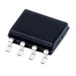
| 描述 | IC OPAMP CFA 1.7GHZ 8SOIC |
| 产品分类 | Linear - Amplifiers - Instrumentation, OP Amps, Buffer Amps |
| 品牌 | Texas Instruments |
| 数据手册 | |
| 产品图片 |
|
| 产品型号 | LMH6702MA |
| rohs | 含铅 / 不符合限制有害物质指令(RoHS)规范要求 |
| 产品系列 | - |
| 产品培训模块 | http://www.digikey.cn/PTM/IndividualPTM.page?site=cn&lang=zhs&ptm=30123http://www.digikey.cn/PTM/IndividualPTM.page?site=cn&lang=zhs&ptm=30126http://www.digikey.cn/PTM/IndividualPTM.page?site=cn&lang=zhs&ptm=30127 |
| 供应商器件封装 | 8-SOIC |
| 制造商产品页 | http://www.ti.com/general/docs/suppproductinfo.tsp?distId=10&orderablePartNumber=LMH6702MA |
| 包装 | 管件 |
| 压摆率 | 3100 V/µs |
| 增益带宽积 | - |
| 安装类型 | 表面贴装 |
| 封装/外壳 | 8-SOIC(0.154",3.90mm 宽) |
| 工作温度 | -40°C ~ 85°C |
| 放大器类型 | 电流反馈 |
| 标准包装 | 95 |
| 电压-电源,单/双 (±) | 10 V ~ 12 V, ±5 V ~ 6 V |
| 电压-输入失调 | 1mV |
| 电流-电源 | 12.5mA |
| 电流-输入偏置 | 6µA |
| 电流-输出/通道 | 80mA |
| 电路数 | 1 |
| 设计资源 | http://www.digikey.com/product-highlights/cn/zh/texas-instruments-webench-design-center/3176 |
| 输出类型 | - |


- 商务部:美国ITC正式对集成电路等产品启动337调查
- 曝三星4nm工艺存在良率问题 高通将骁龙8 Gen1或转产台积电
- 太阳诱电将投资9.5亿元在常州建新厂生产MLCC 预计2023年完工
- 英特尔发布欧洲新工厂建设计划 深化IDM 2.0 战略
- 台积电先进制程称霸业界 有大客户加持明年业绩稳了
- 达到5530亿美元!SIA预计今年全球半导体销售额将创下新高
- 英特尔拟将自动驾驶子公司Mobileye上市 估值或超500亿美元
- 三星加码芯片和SET,合并消费电子和移动部门,撤换高东真等 CEO
- 三星电子宣布重大人事变动 还合并消费电子和移动部门
- 海关总署:前11个月进口集成电路产品价值2.52万亿元 增长14.8%


PDF Datasheet 数据手册内容提取
Product Sample & Technical Tools & Support & Folder Buy Documents Software Community LMH6702 SNOSA03H–NOVEMBER2002–REVISEDMAY2016 LMH6702 1.7-GHz Ultra-Low Distortion Wideband Op Amp 1 Features 3 Description V = ±5 V, T = 25°C, A = 2V/V, R = 100 Ω, The LMH6702 is a very wideband, DC-coupled 1 S A V L V =2V ,TypicalUnlessNoted: monolithic operational amplifier designed specifically OUT PP for wide dynamic range systems requiring exceptional • 2ndand3rdHarmonics(5MHz,SOT-23)−100/−96 signal fidelity. Benefitting from current feedback dBc architecture,theLMH6702offersunitygainstabilityat • −3-dBBandwidth(V =0.5V )1.7GHz exceptional speed without need for external OUT PP compensation. • LowNoise1.83nV/√Hz • FastSettlingto0.1%13.4ns Withits720-MHzbandwidth(A =2V/V,V =2V ), V O PP 10-bit distortion levels through 60-MHz (R = 100 Ω), • FastSlewRate3100V/μs L 1.83-nV/√Hz input referred noise and 12.5-mA supply • SupplyCurrent12.5mA current, the LMH6702 is the ideal driver or buffer for • OutputCurrent80mA high-speedflashA-DandD-Aconverters. • LowIntermodulationDistortion(75MHz) −67dBc Wide dynamic range systems such as radar and • ImprovedReplacementforCLC409andCLC449 communication receivers that require a wideband amplifier offering exceptional signal purity will find the 2 Applications low input referred noise and low harmonic and intermodulation distortion of the LMH6702 an • FlashA-DDriver attractivehighspeedsolution. • D-ATransimpedanceBuffer The LMH6702 is constructed using VIP10™ • WideDynamicRangeIFAmp complimentary bipolar process and proven current • RadarandCommunicationReceivers feedback architecture. The LMH6702 is available in • LineDriver SOICandSOT-23packages. • HighResolutionVideo DeviceInformation(1) PARTNUMBER PACKAGE BODYSIZE(NOM) SOIC(8) 4.90mm×3.91mm LMH6702 SOT-23(5) 2.90mm×1.60mm (1) For all available packages, see the orderable addendum at theendofthedatasheet. InvertingFrequencyResponse HarmonicDistortionvsLoadandFrequency 1 -30 GAIN AV = -1 -40 0 AV = -2 -80 -45 -50 HD2, RL = 1 k: -1 -130 -55 PHASE -2 -180 -60 )Bd( n -3 -230 °)( esa )cB --7605 HD2, RL = 100 : iaG -4 AV = -4 -280 hP d( D -75 HD3, RL = 100 : H -80 -5 -330 -85 AV = -10 -90 -6 -380 -95 HD3, RL = 1 k: -7 -430 -100 1M 10M 100M 1G -105 Frequency (Hz) 1M 10M 100M Frequency (Hz) 1 An IMPORTANT NOTICE at the end of this data sheet addresses availability, warranty, changes, use in safety-critical applications, intellectualpropertymattersandotherimportantdisclaimers.PRODUCTIONDATA.
LMH6702 SNOSA03H–NOVEMBER2002–REVISEDMAY2016 www.ti.com Table of Contents 1 Features.................................................................. 1 7.3 DeviceFunctionalModes........................................12 2 Applications........................................................... 1 8 ApplicationandImplementation........................ 13 3 Description............................................................. 1 8.1 ApplicationInformation............................................13 4 RevisionHistory..................................................... 2 8.2 TypicalApplication .................................................13 5 PinConfigurationandFunctions......................... 3 9 PowerSupplyRecommendations...................... 15 6 Specifications......................................................... 4 10 Layout................................................................... 15 6.1 AbsoluteMaximumRatings......................................4 10.1 LayoutGuidelines.................................................15 6.2 ESDRatings..............................................................4 10.2 LayoutExample....................................................16 6.3 RecommendedOperatingConditions.......................4 11 DeviceandDocumentationSupport................. 17 6.4 ThermalInformation..................................................4 11.1 DocumentationSupport .......................................17 6.5 ElectricalCharacteristics...........................................5 11.2 CommunityResources..........................................17 6.6 TypicalCharacteristics..............................................7 11.3 Trademarks...........................................................17 7 DetailedDescription............................................ 11 11.4 ElectrostaticDischargeCaution............................17 7.1 Overview.................................................................11 11.5 Glossary................................................................17 7.2 FeatureDescription.................................................11 12 Mechanical,Packaging,andOrderable Information........................................................... 17 4 Revision History NOTE:Pagenumbersforpreviousrevisionsmaydifferfrompagenumbersinthecurrentversion. ChangesfromRevisionG(October2014)toRevisionH Page • UpdatedThermalInformation................................................................................................................................................. 4 • Changednon-invertinginputbias(withnotestconditions)currentmaximumvaluefrom±15µAto–15µA........................ 6 • Changednon-invertinginputbias(-40≤T ≤85)currentmaximumvaluefrom±21µAto–21µA...................................... 6 J • AddedCommunityResourcessection................................................................................................................................. 17 ChangesfromRevisionF(March2013)toRevisionG Page • Added,updated,orrenamedthefollowingsections:DeviceInformation;Specifications;Applicationand Implementation;PowerSupplyRecommendations;Layout;DeviceandDocumentationSupport;Mechanical, Packaging,andOrderingInformation .................................................................................................................................... 1 • Changed±5Vto±4VinRecommendedOperatingConditions............................................................................................ 4 ChangesfromRevisionE(March2013)toRevisionF Page • ChangedlayoutofNationalDataSheettoTIformat............................................................................................................. 1 2 SubmitDocumentationFeedback Copyright©2002–2016,TexasInstrumentsIncorporated ProductFolderLinks:LMH6702
LMH6702 www.ti.com SNOSA03H–NOVEMBER2002–REVISEDMAY2016 5 Pin Configuration and Functions DBVPackage 5-PinSOT-23 DPackage TopView 8-PinSOIC TopView OUT 1 5 V+ N/C 1 8 N/C -IN 2 - 7 V+ - 2 V + - +IN 3 + 6 OUT +IN 3 4 -IN V- 4 5 N/C NC:Nointernalconnection PinFunctions PIN NUMBER I/O DESCRIPTION NAME D DBV -IN 2 4 I Invertinginputvoltage +IN 3 3 I Non-invertinginputvoltage N/C 1,5,8 – – Noconnection OUT 6 1 O Output V- 4 2 I Negativesupply V+ 7 5 I Positivesupply Copyright©2002–2016,TexasInstrumentsIncorporated SubmitDocumentationFeedback 3 ProductFolderLinks:LMH6702
LMH6702 SNOSA03H–NOVEMBER2002–REVISEDMAY2016 www.ti.com 6 Specifications 6.1 Absolute Maximum Ratings overoperatingfree-airtemperaturerange(unlessotherwisenoted) (1)(2) MIN MAX UNIT V ±6.75 V S I See(3) OUT Commonmodeinputvoltage V−toV+ V Maximumjunctiontemperature 150 °C Storagetemperature −65 150 °C Infraredorconvection(20s) 235 °C Solderinginformation Wavesoldering(10s) 260 °C (1) StressesbeyondthoselistedunderAbsoluteMaximumRatingsmaycausepermanentdamagetothedevice.Thesearestressratings only,whichdonotimplyfunctionaloperationofthedeviceattheseoranyotherconditionsbeyondthoseindicatedunderRecommended OperatingConditions.Exposuretoabsolute-maximum-ratedconditionsforextendedperiodsmayaffectdevicereliability. (2) IfMilitary/Aerospacespecifieddevicesarerequired,pleasecontacttheTISalesOffice/Distributorsforavailabilityandspecifications. (3) Themaximumoutputcurrent(I )isdeterminedbydevicepowerdissipationlimitations. OUT 6.2 ESD Ratings VALUE UNIT Human-bodymodel(HBM),perANSI/ESDA/JEDECJS-001(1) ±2000 V Electrostaticdischarge V (ESD) MachineModel(MM),perJEDECspecificationJESD22-C101,allpins(2) ±200 (1) Humanbodymodel:1.5kΩinserieswith100pF.JEDECdocumentJEP155statesthat2000-VHBMallowssafemanufacturingwitha standardESDcontrolprocess.Manufacturingwithlessthan2000-VHBMispossiblewiththenecessaryprecautions.Pinslistedas ±2000Vmayactuallyhavehigherperformance. (2) Machinemodel:0Ωinserieswith200pF.JEDECdocumentJEP157statesthat200-VMMallowssafemanufacturingwithastandard ESDcontrolprocess.Manufacturingwithlessthan200-VMMispossiblewiththenecessaryprecautions.Pinslistedas±200Vmay actuallyhavehigherperformance. 6.3 Recommended Operating Conditions overoperatingfree-airtemperaturerange(unlessotherwisenoted)(1) MIN MAX UNIT Operatingtemperature −40 85 °C Nominalsupplyvoltage ±4 ±6 V (1) AbsoluteMaximumRatingsindicatelimitsbeyondwhichdamagetothedevicemayoccur.OperatingRatingsindicateconditionsfor whichthedeviceisintendedtobefunctional,butspecificperformanceisnotensured.Forensuredspecifications,seetheElectrical Characteristicstables. 6.4 Thermal Information LMH6702 THERMALMETRIC(1) DBV(SOT-23) D(SOIC) UNIT 5PINS 8PINS R Junction-to-ambientthermalresistance 182 133 °C/W θJA R Junction-to-case(top)thermalresistance 139 79 °C/W θJC(top) R Junction-to-boardthermalresistance 40 73 °C/W θJB ψ Junction-to-topcharacterizationparameter 28 28 °C/W JT ψ Junction-to-boardcharacterizationparameter 40 73 °C/W JB (1) Formoreinformationabouttraditionalandnewthermalmetrics,seetheSemiconductorandICPackageThermalMetricsapplication report(SPRA953). 4 SubmitDocumentationFeedback Copyright©2002–2016,TexasInstrumentsIncorporated ProductFolderLinks:LMH6702
LMH6702 www.ti.com SNOSA03H–NOVEMBER2002–REVISEDMAY2016 6.5 Electrical Characteristics atA =2,V =±5V,R =100Ω,R =237Ω(unlessotherwisenoted)(1) V S L F PARAMETER TESTCONDITIONS MIN(2) TYP(3) MAX(2) UNIT FREQUENCYDOMAINPERFORMANCE SSBW V =0.5V 1700 SM OUT PP SSBW V =2V 720 LG OUT PP -3-dBBandwidth MHz LSBW V =4V 480 LG OUT PP SSBW V =2V ,A =+10 140 HG OUT PP V GF 0.1-dBgainflatness V =2V 120 MHz 0.1dB OUT PP LPD Linearphasedeviation DCto100MHz 0.09 deg R =150Ω,3.58MHz 0.024% L DG Differentialgain R =150Ω,4.43MHz 0.021% L R =150Ω,3.58MHz 0.004 L DP Differentialphase deg R =150Ω,4.43MHz 0.007 L TIMEDOMAINRESPONSE 2-VStep,TRS 0.87 t Risetime ns R 2-VStep,TRL 0.77 6-VStep,TRS 1.70 t Falltime ns F 6-VStep,TRL 1.70 OS Overshoot 2-VStep 0% SR Slewrate 6V ,40%to60%(4) 3100 V/µs PP T Settlingtimeto0.1% 2-VStep 13.4 ns s DISTORTIONANDNOISERESPONSE 2V ,5MHz(5)(SOT-23) −100 PP HD2L dBc 2V ,5MHz(5)(SOIC) −87 PP 2V ,20MHz(5)(SOT-23) −79 HD2 2ndHarmonicdistortion PP dBc 2V ,20MHz(5)(SOIC) −72 PP 2V ,60MHz(5)(SOT-23) −63 PP HD2H dBc 2V ,60MHz(5)(SOIC) −64 PP 2V ,5MHz(5)(SOT-23) −96 PP HD3L dBc 2V ,5MHz(5)(SOIC) −98 PP 2V ,20MHz(5)(SOT-23) −88 HD3 3rdHarmonicdistortion PP dBc 2V ,20MHz(5)(SOIC) −82 PP 2V ,60MHz(5)(SOT-23) −70 PP HD3H dBc 2V ,60MHz(5)(SOIC) −65 PP OIM3 IMD 75MHz,P =10dBm/tone −67 dBc O V Inputreferredvoltagenoise >1MHz 1.83 nV/√Hz N Inputreferredinverting >1MHz I 18.5 pA/√Hz N noisecurrent Inputreferrednon-inverting >1MHz I 3.0 pA/√Hz NN noisecurrent SNF Totalinputnoisefloor >1MHz −158 dBm 1Hz INV Totalintegratedinputnoise 1MHzto150MHz 35 µV (1) ElectricalTablevaluesapplyonlyforfactorytestingconditionsatthetemperatureindicated.Factorytestingconditionsresultinvery limitedself-heatingofthedevicesuchthatT =T .Noguaranteeofparametricperformanceisindicatedintheelectricaltablesunder J A conditionsofinternalself-heatingwhereT >T .Min/Maxratingsarebasedonproductiontestingunlessotherwisespecified. J A (2) Alllimitsareensuredbytestingorstatisticalanalysis. (3) Typicalnumbersarethemostlikelyparametricnorm. (4) SlewRateistheaverageoftherisingandfallingedges. (5) Harmonicdistortionisstronglyinfluencedbypackagetype(SOT-23orSOIC).SeeApplicationNotesectionunderHarmonicDistortion formoreinformation. Copyright©2002–2016,TexasInstrumentsIncorporated SubmitDocumentationFeedback 5 ProductFolderLinks:LMH6702
LMH6702 SNOSA03H–NOVEMBER2002–REVISEDMAY2016 www.ti.com Electrical Characteristics (continued) atA =2,V =±5V,R =100Ω,R =237Ω(unlessotherwisenoted)(1) V S L F PARAMETER TESTCONDITIONS MIN(2) TYP(3) MAX(2) UNIT STATIC,DCPERFORMANCE ±1.0 ±4.5 V Inputoffsetvoltage mV IO -40≤T ≤85 ±6.0 J DV Inputoffsetvoltageaverage See(6) −13 µV/°C IO drift −6 –15 I Inputbiascurrent Non-Inverting(7) µA BN -40≤T ≤85 –21 J DI Inputbiascurrentaverage Non-Inverting(6) +40 nA/°C BN drift −8 ±30 I Inputbiascurrent Inverting(7) µA BI -40≤T ≤85 ±34 J DI Inputbiascurrentaverage Inverting(6) −10 nA/°C BI drift 47 52 PSRR Powersupplyrejectionratio DC dB -40≤T ≤85 45 J Commonmoderejection 45 48 CMRR DC dB ration -40≤T ≤85 44 J 11.0 12.5 16.1 I Supplycurrent R =∞ mA CC L -40≤T ≤85 10.0 17.5 J MISCELLANEOUSPERFORMANCE R Inputresistance Non-Inverting 1.4 MΩ IN C Inputcapacitance Non-Inverting 1.6 pF IN R Outputresistance ClosedLoop 30 mΩ OUT ±3.3 ±3.5 V Outputvoltagerange R =100Ω V OL L -40≤T ≤85 ±3.2 J CMIR Inputvoltagerange CommonMode ±1.9 ±2.2 V I Outputcurrent 50 80 mA O (6) Driftdeterminedbydividingthechangeinparameterattemperatureextremesbythetotaltemperaturechange. (7) Negativeinputcurrentimpliescurrentflowingoutofthedevice. 6 SubmitDocumentationFeedback Copyright©2002–2016,TexasInstrumentsIncorporated ProductFolderLinks:LMH6702
LMH6702 www.ti.com SNOSA03H–NOVEMBER2002–REVISEDMAY2016 6.6 Typical Characteristics T =25°C,V =±5V,R =100Ω,R =237Ω(unlessotherwisenoted) A S L f 1 150 1 -30 GAIN AV = +1 GAIN AV = -1 0 100 0 AV = -2 -80 -1 AV = +2 50 -1 -130 -2 PHASE AV = +4 0 -2 PHASE -180 )Bd( niaG --43 AV = +4 --51000)° (esahP )Bd( niaG --43 AV = -4 --228300 °) (esahP AV = +2 -5 -150 -5 -330 AV = +1 AV = -10 -6 -200 -6 -380 AV = +10 -7 -250 -7 -430 1M 10M 100M 1G 1M 10M 100M 1G Frequency (Hz) Frequency (Hz) V0=2Vpp RL=100Ω RF=237Ω VOUT=2VPP RF=237Ω RL=100Ω Figure1.Non-InvertingFrequencyResponse Figure2.InvertingFrequencyResponse 1 1 150 GAIN GAIN 100 : 0 0 100 -1 -1 50 -2 PHASE )Bd( niaG ---543 PHASE -054 °) (esahP )Bd( niaG ---432 1 k: 50 : 1 k: --015000 )° (esahP -6 -108 -5 -150 -7 -162 100 : -8 -216 -6 50 : -200 -9 -270 -7 -250 10M 100M 1G 10G 0 200M 400M 600M 800M 1G Frequency (Hz) Frequency (Hz) VOUT=0.5VPP AV=2 RF=232Ω AV=2 VO=2VPP RF=237Ω Figure3.SmallSignalBandwidth Figure4.FrequencyResponseforVariousR s,A =2 L V 1 150 1.5 GAIN 0 100 1 -1 50 PHASE -2 1 k: 0 0.5 AV = +2 )Bd( niaG -3 50 : -50 )° (esahP )V( VTUO 0 -4 -100 50 : -0.5 AV = -2 -5 -150 -1 -6 -200 -7 100 : -250 -1.5 0 100M 200M 300M 400M 500M 0 2 4 6 8 10 12 14 Frequency (Hz) Time (ns) AV=4 VO=2VPP RF=237Ω VO=2VPP RL=100Ω Figure5.FrequencyResponseforVariousR s,A =4 Figure6.StepResponse,2V L V PP Copyright©2002–2016,TexasInstrumentsIncorporated SubmitDocumentationFeedback 7 ProductFolderLinks:LMH6702
LMH6702 SNOSA03H–NOVEMBER2002–REVISEDMAY2016 www.ti.com Typical Characteristics (continued) T =25°C,V =±5V,R =100Ω,R =237Ω(unlessotherwisenoted) A S L f 4 1 3 2 )V( T 01 )%( ro 0.1 UO rrE V -1 gn iltte 0.01 -2 S -3 -4 0.001 0 10 20 30 40 50 60 1 10 100 1k Time (ns) Time (ns) AV=2 VOUT=6VPP RL=100Ω RL=100Ω Figure7.StepResponse,6V Figure8.PercentSettlingvsTime PP -40 -40 -45 -50 HD2, RL = 1 k: -50 75 MHz -55 -60 -60 )cB --7605 HD2, RL = 100 : )cB -70 d( DH --8705 HD3, RL = 100 : d( PS -80 -85 -90 50 MHz -90 -95 HD3, RL = 1 k: -100 -100 25 MHz -105 -110 1M 10M 100M -5 -3 -1 1 3 5 Frequency (Hz) Test Tone Power at 50 : Load (dBm) 2V A =2 R =237Ω PP V F A =2 R =100Ω R =237Ω V L F Figure9.HarmonicDistortionvsLoadandFrequency Figure10.2Tone3rdOrderSpuriousLevel (SOICPackage) (SOICPackage) 100 25 -50 90 0.05% SETTLING 60MHz -60 80 20 70 20MHz )s -70 :) 60 15 n (em )cB (R S 345000 0.1% SETTLING RS 10 iT gniltteS d( DH --9800 10MHz 20 5 -100 10 5MHz 0 0 -110 1 10 100 1k 10k -10 -5 0 5 10 15 20 CL (pF) POUT (dBm) AV=-1 RL=1kΩ AV=2 RF=237Ω RL=100Ω Figure11.R andSettlingTimevsC Figure12.HD2vsOutputPower(Across100Ω) S L (SOICPackage) 8 SubmitDocumentationFeedback Copyright©2002–2016,TexasInstrumentsIncorporated ProductFolderLinks:LMH6702
LMH6702 www.ti.com SNOSA03H–NOVEMBER2002–REVISEDMAY2016 Typical Characteristics (continued) T =25°C,V =±5V,R =100Ω,R =237Ω(unlessotherwisenoted) A S L f -50 0.5 60 MHz UNIT 1 -60 0 -0.5 -70 -1 20 MHz )cB -80 )Vm -1.5 d( DH -90 ( VSO -2 UNIT 2 -100 10 MHz 5 MHz -2.5 UNIT 3 -3 -110 -3.5 -120 -4 -10 -5 0 5 10 15 20 -40 -15 10 35 60 85 110 135 POUT (dBm) TEMPERATURE (°C) A =2 R =237Ω R =100Ω V F L Figure13.HD3vsOutputPower(Across100Ω) Figure14.InputOffsetfor3RepresentativeUnits (SOICPackage) 10 -4 UNIT 3 8 -5 6 -6 UNIT 3 4 2 -7 )A )A UNIT 2 µ( IIB -20 UNIT 2 UNIT 1 µ( INB --98 -4 -10 -6 UNIT 1 -8 -11 -10 -12 -40 -15 10 35 60 85 110 135 -40 -15 10 35 60 85 110 135 TEMPERATURE (°C) TEMPERATURE (°C) Figure15.InvertingInputBias Figure16.Non-InvertingInputBiasfor3Representative for3RepresentativeUnits Units 1000 70 15 + PSRR 60 5 Hz) Hz) 50 -5 NOISE VOLTAGE (nV/ NOISE CURRENT (pA/ 11000 INVENROTIN NC-UGINR CVRUEERRNRTTIENNGT )Bd( RRSP/RRMC 324000 CMRR - PSRR ---312555 )R( goL 02O RO VOLTAGE 10 -45 1 100 1k 10k 100k 1M 10M 0 -55 1k 10k 100k 1M 10M 100M FREQUENCY (Hz) Frequency (Hz) V =±5V R =100Ω S L Figure17.Noise Figure18.CMRR,PSRR,R OUT Copyright©2002–2016,TexasInstrumentsIncorporated SubmitDocumentationFeedback 9 ProductFolderLinks:LMH6702
LMH6702 SNOSA03H–NOVEMBER2002–REVISEDMAY2016 www.ti.com Typical Characteristics (continued) T =25°C,V =±5V,R =100Ω,R =237Ω(unlessotherwisenoted) A S L f 120 220 0.03 0.006 110 200 100 180 0.02 0.004 DP 90 160 MAG 0.01 0.002 )Bd( niaG867000 111402000 °) (esahP )%( GD 0 0 )(° PD 50 PHASE 80 -0.01 -0.002 DG 40 60 -0.02 -0.004 30 40 20 20 -0.03 -0.006 10k 100k 1M 10M 100M 1G -1.5-1.2-0.9-0.6-0.3 0 0.3 0.6 0.9 1.21.5 Frequency (Hz) VOUT (V) VS=±5V RL=100Ω RF=237Ω RL=150Ω Figure19.Transimpedance Figure20.DG/DP(NTSC) 0.03 0.009 0.02 0.006 DP 0.01 0.003 )%( GD 0 0 )°( PD -0.01 -0.003 DG -0.02 -0.006 -0.03 -0.009 -1.5-1.2-0.9-0.6-0.3 0 0.3 0.6 0.91.2 1.5 VOUT (V) R =237Ω R =150Ω F L Figure21.DG/DP(PAL) 10 SubmitDocumentationFeedback Copyright©2002–2016,TexasInstrumentsIncorporated ProductFolderLinks:LMH6702
LMH6702 www.ti.com SNOSA03H–NOVEMBER2002–REVISEDMAY2016 7 Detailed Description 7.1 Overview The LMH6702 has been optimized for exceptionally low harmonic distortion while driving very demanding resistive or capacitive loads. Generally, when used as the input amplifier to very high speed flash ADCs, the distortions introduced by the converter will dominate over the low LMH6702 distortions shown in Typical Characteristics. 7.2 Feature Description 7.2.1 HarmonicDistortion The capacitor C , shown across the supplies in Figure 24 and Figure 25, is critical to achieving the lowest 2nd SS harmonic distortion. For absolute minimum distortion levels, it is also advisable to keep the supply decoupling currents (ground connections to C , and C in Figure 24 and Figure 25) separate from the ground POS NEG connections to sensitive input circuitry (such as R , R , and R ground connections). Splitting the ground plane G T IN in this fashion and separately routing the high frequency current spikes on the decoupling caps back to the power supply (similar to Star Connection layout technique) ensures minimum coupling back to the input circuitry andresultsinbestharmonicdistortionresponse(especially2ndorderdistortion). If this layout technique has not been observed on a particular application board, designer may actually find that supplydecouplingcapscouldadverselyaffectHD2performancebyincreasingthecouplingphenomenonalready mentioned. Figure 22 shows actual HD2 data on a board where the ground plane is shared between the supply decoupling capacitors and the rest of the circuit. Once these capacitors are removed, the HD2 distortion levels reducesignificantly,especiallybetween10MHzto20MHz,asshowninFigure22: -30 -40 CPOS & CNEG -50 INCLUDED )cB d ( 2D -60 CPOS & CNEG H REMOVED -70 -80 -90 1 10 100 Frequency (MHz) Figure22. DecouplingCurrentAdverseEffectonaBoardwithSharedGroundPlane At these extremely low distortion levels, the high frequency behavior of decoupling capacitors themselves could be significant. In general, lower value decoupling caps tend to have higher resonance frequencies making them more effective for higher frequency regions. A particular application board which has been laid out correctly with groundreturnssplittominimizecoupling,wouldbenefitthemostbyhavinglowvalueandhighervaluecapacitors paralleledtotakeadvantageoftheeffectivebandwidthofeachandextendlowdistortionfrequencyrange. Another important variable in getting the highest fidelity signal from the LMH6702 is the package itself. As already noted, coupling between high frequency current transients on supply lines and the device input can lead to excess harmonic distortion. An important source of this coupling is in fact through the device bonding wires. A smallerpackage,ingeneral,willhaveshorterbondingwiresandthereforelowercoupling.Thisistrueinthecase of the SOT-23 compared to the SOIC package where a marked improvement in HD can be measured in the SOT-23package.Figure23showstheHDcomparingSOT-23toSOICpackage: Copyright©2002–2016,TexasInstrumentsIncorporated SubmitDocumentationFeedback 11 ProductFolderLinks:LMH6702
LMH6702 SNOSA03H–NOVEMBER2002–REVISEDMAY2016 www.ti.com Feature Description (continued) -60 HD2, SOIC -65 -70 -75 HD2, SOT23 )cB -80 d( 2 -85 D H -90 HD3, SOIC -95 HD3, SOT23 -100 -105 -110 1 10 100 Frequency (MHz) Figure23. SOICandSOT-23PackagesDistortionTermsCompared The LMH6702 data sheet shows both SOT-23 and SOIC data in Electrical Characteristics to aid in selecting the rightpackage.TypicalCharacteristicsshowsSOICpackageplotsonly. 7.3 Device Functional Modes 7.3.1 2-Tone3rd OrderIntermodulation Figure 10 shows a relatively constant difference between the test power level and the spurious level with the difference depending on frequency. The LMH6702 does not show an intercept type performance, (where the relative spurious levels change at a 2X rate versus the test tone powers), due to an internal full power bandwidth enhancement circuit that boosts the performance as the output swing increases while dissipating negligible quiescent power under low output power conditions. This feature enhances the distortion performance and full powerbandwidthtomatchthatofmuchhigherquiescentsupplycurrentparts. 7.3.2 DCAccuracyandNoise The example in Equation 1 shows the output offset computation equation for the non-inverting configuration usingthetypicalbiascurrentandoffsetspecificationsforA =2: V OutputOffset: V =(±I ·R ±V )(1+R /R )±I ·R O BN IN IO F G BI F where • R istheequivalentinputimpedanceonthenon-invertinginput. (1) IN ExamplecomputationforA =+2,R =237Ω,R =25Ω: V F IN V =(±6μA×25Ω±1mV)(1+237/237)±8μA×237=±4.20mV (2) O A good design, however, should include a worst case calculation using min/max numbers in the data sheet tables,inordertoensureworstcaseoperation. Further improvement in the output offset voltage and drift is possible using the composite amplifiers described in Application Note OA--07, Current Feedback Op Amp Applications Circuit Guide (SNOA365). The two input bias currents are physically unrelated in both magnitude and polarity for the current feedback topology. It is not possible, therefore, to cancel their effects by matching the source impedance for the two inputs (as is commonly doneformatchedinputbiascurrentdevices). The total output noise is computed in a similar fashion to the output offset voltage. Using the input noise voltage and the two input noise currents, the output noise is developed through the same gain equations for each term but combined as the square root of the sum of squared contributing elements. See Application Note OA-12, Noise Analysis for Comlinear Amplifiers (SNOA375) for a full discussion of noise calculations for current feedbackamplifiers. 12 SubmitDocumentationFeedback Copyright©2002–2016,TexasInstrumentsIncorporated ProductFolderLinks:LMH6702
LMH6702 www.ti.com SNOSA03H–NOVEMBER2002–REVISEDMAY2016 8 Application and Implementation NOTE Information in the following applications sections is not part of the TI component specification, and TI does not warrant its accuracy or completeness. TI’s customers are responsible for determining suitability of components for their purposes. Customers should validateandtesttheirdesignimplementationtoconfirmsystemfunctionality. 8.1 Application Information The LMH6702 achieves its excellent pulse and distortion performance by using the current feedback topology. The loop gain for a current feedback op amp, and hence the frequency response, is predominantly set by the feedback resistor value. The LMH6702 is optimized for use with a 237-Ω feedback resistor. Using lower values canleadtoexcessiveringinginthepulseresponsewhileahighervaluewilllimitthebandwidth. 8.2 Typical Application 8.2.1 FeedbackResistor The LMH6702 achieves its excellent pulse and distortion performance by using the current feedback topology. The loop gain for a current feedback op amp, and hence the frequency response, is predominantly set by the feedback resistor value. The LMH6702 is optimized for use with a 237-Ω feedback resistor. Using lower values canleadtoexcessiveringinginthepulseresponsewhileahighervaluewilllimitthebandwidth. +5V 6.8µF .01µF AV = 1 +RF/RG = VOUT/VIN VIN 3 +7 CPOS RIN 0.C1µSFS LMH6702 6 VOUT - 2 4 CNEG RF .01µF RG 6.8µF -5V Figure24. RecommendedNon-InvertingGainCircuit +5V 6.8µF .01µF AV = RRGF=VVOIUNT 3 +7 CPOS 25: 0.C1µSFS LMH6702 6 VOUT - 2 4 CNEG VIN RG .01µF RF RT 6.8µF SYEIELLEDC DTE RSTI RTEOD -5V RIN = RT||RG Figure25. RecommendedInvertingGainCircuit Copyright©2002–2016,TexasInstrumentsIncorporated SubmitDocumentationFeedback 13 ProductFolderLinks:LMH6702
LMH6702 SNOSA03H–NOVEMBER2002–REVISEDMAY2016 www.ti.com Typical Application (continued) 8.2.2 DesignRequirements The exceptional performance and uniquely targeted superior technical specifications of the LMH6702 make it a natural choice for high speed data acquisition applications as a front end amplifier driving the input of a high performanceADC.Ofthesespecifications,thefollowingcanbediscussedinmoredetail: 1. A bandwidth of 1.7 GHz and relative insensitivity of bandwidth to closed loop gain (characteristic of Current Feedbackarchitecturewhencomparedtothetraditionalvoltagefeedbackarchitecture)asshowninFigure1. 2. Ultra-low distortion approaching -87 dBc at the lower frequencies and exceptional noise performance (see Figure9 andFigure17). 3. Fastsettlinginlessthan20ns(seeFigure27). As the input of an ADC could be capacitive in nature and could also alternate in capacitance value during a typical acquisition cycle, the driver amplifier (LMH6702 in this case) should be designed so that it avoids instability,peaking,orotherundesirableartifacts. For Capacitive Load Drive, see Figure 26, which shows a typical application using the LMH6702 to drive an ADC. ADC + RS LMH6702 - CIN Figure26. InputAmplifiertoADC 8.2.3 DetailedDesignProcedure The series resistor, R , between the amplifier output and the ADC input is critical to achieving best system S performance. This load capacitance, if applied directly to the output pin, can quickly lead to unacceptable levels of ringing in the pulse response. Figure 27 in Application Curve (R and Settling Time vs C ) is an excellent S L starting point for selecting R . The value derived in that plot minimizes the step settling time into a fixed discrete S capacitive load with the output driving a very light resistive load (1 kΩ). Sensitivity to capacitive loading is greatly reduced once the output is loaded more heavily. Therefore, for cases where the output is heavily loaded, R S valuemaybereduced.Theexactvaluemaybestbedeterminedexperimentallyforthesecases. In applications where the LMH6702 is replacing the CLC409, care must be taken when the device is lightly loaded and some capacitance is present at the output. Due to the much higher frequency response of the LMH6702 compared to the CLC409, there could be increased susceptibility to low value output capacitance (parasitic or inherent to the board layout or otherwise being part of the output load). As already mentioned, this susceptibility is most noticeable when the LMH6702's resistive load is light. Parasitic capacitance can be minimized by careful lay out. Addition of an output snubber R-C network will also help by increasing the high frequencyresistiveloading. Referring back to Figure 26, it must be noted that several additional constraints should be considered in driving the capacitive input of an ADC. There is an option to increase R , band-limiting at the ADC input for either noise S or Nyquist band-limiting purposes. However, increasing R too much can induce an unacceptably large input S glitch due to switching transients coupling through from the convert signal. Also, C is oftentimes a voltage IN dependent capacitance. This input impedance non-linearity will induce distortion terms that will increase as R is S increased. Only slight adjustments up or down from the recommended R value should therefore be attempted in S optimizingsystemperformance. 14 SubmitDocumentationFeedback Copyright©2002–2016,TexasInstrumentsIncorporated ProductFolderLinks:LMH6702
LMH6702 www.ti.com SNOSA03H–NOVEMBER2002–REVISEDMAY2016 Typical Application (continued) 8.2.4 ApplicationCurve 100 25 90 0.05% SETTLING 80 20 70 )s :) 60 15 n (em (R S 345000 0.1% SETTLING RS 10 iT gniltteS 20 5 10 0 0 1 10 100 1k 10k CL (pF) A =-1 R =1kΩ V L Figure27.R andSettlingTimevsC S L 9 Power Supply Recommendations The LMH6702 can operate off a single supply or with dual supplies as long as the input CM voltage range (CMIR) has the required headroom to either supply rail. Supplies should be decoupled with low inductance, often ceramic, capacitors to ground less than 0.5 inches from the device pins. The use of ground plane is recommended, and as in most high speed devices, it is advisable to remove ground plane close to device sensitivepinssuchastheinputs. 10 Layout 10.1 Layout Guidelines Generally, a good high frequency layout will keep power supply and ground traces away from the inverting input and output pins. Parasitic capacitances on these nodes to ground will cause frequency response peaking and possible circuit oscillations. See Frequent Faux Pas in Applying Wideband Current Feedback Amplifiers, Application Note OA-15 (SNOA367). Texas Instruments suggests the following evaluation boards as a guide for highfrequencylayoutandasanaidindevicetestingandcharacterization.SeeTable1fordetails. The LMH6702 evaluation board(s) is a good example of high frequency layout techniques as a reference. Generalhigh-speed,signal-pathlayoutsuggestionsinclude: • Continuous ground planes are preferred for signal routing with matched impedance traces for longer runs. However, open up both ground and power planes around the capacitive sensitive input and output device pins as shown in Figure 28. After the signal is sent into a resistor, parasitic capacitance becomes more of a bandlimitingissueandlessofastabilityissue. • Use good, high-frequency decoupling capacitors (0.1 μF) on the ground plane at the device power pins as shown in Figure 28. Higher value capacitors (2.2 μF) are required, but may be placed further from the device power pins and shared among devices. For best high-frequency decoupling, consider X2Y supply-decoupling capacitorsthatofferamuchhigherself-resonancefrequencyoverstandardcapacitors. • When using differential signal routing over any appreciable distance, use microstrip layout techniques with matchedimpedancetraces. • The input summing junction is very sensitive to parasitic capacitance. Connect any Rf, and Rg elements into the summing junction with minimal trace length to the device pin side of the resistor, as shown in Figure 29. Theothersideoftheseelementscanhavemoretracelengthifneededtothesourceortoground. Copyright©2002–2016,TexasInstrumentsIncorporated SubmitDocumentationFeedback 15 ProductFolderLinks:LMH6702
LMH6702 SNOSA03H–NOVEMBER2002–REVISEDMAY2016 www.ti.com 10.2 Layout Example Figure28. LMH6702EvaluationBoardLayer1 Figure29. LMH6702EvaluationBoardLayer2 Table1.EvaluationBoardComparison DEVICE PACKAGE EVALUATIONBOARDPARTNUMBER LMH6702MF SOT-23 LMH730216 LMH6702MA SOIC LMH730227 16 SubmitDocumentationFeedback Copyright©2002–2016,TexasInstrumentsIncorporated ProductFolderLinks:LMH6702
LMH6702 www.ti.com SNOSA03H–NOVEMBER2002–REVISEDMAY2016 11 Device and Documentation Support 11.1 Documentation Support 11.1.1 RelatedDocumentation Forrelateddocumentation,seethefollowing: • AbsoluteMaximumRatingsforSoldering(SNOA549) • CurrentFeedbackOpAmpApplicationsCircuitGuide,ApplicationNoteOA--07(SNOA365) • FrequentFauxPasinApplyingWidebandCurrentFeedbackAmplifiers,ApplicationNoteOA-15(SNOA367) • NoiseAnalysisforComlinearAmplifiers,ApplicationNoteOA-12(SNOA375) • SemiconductorandICPackageThermalMetrics(SPRA953) 11.2 Community Resources The following links connect to TI community resources. Linked contents are provided "AS IS" by the respective contributors. They do not constitute TI specifications and do not necessarily reflect TI's views; see TI's Terms of Use. TIE2E™OnlineCommunity TI'sEngineer-to-Engineer(E2E)Community.Createdtofostercollaboration amongengineers.Ate2e.ti.com,youcanaskquestions,shareknowledge,exploreideasandhelp solveproblemswithfellowengineers. DesignSupport TI'sDesignSupport QuicklyfindhelpfulE2Eforumsalongwithdesignsupporttoolsand contactinformationfortechnicalsupport. 11.3 Trademarks VIP10,E2EaretrademarksofTexasInstruments. Allothertrademarksarethepropertyoftheirrespectiveowners. 11.4 Electrostatic Discharge Caution Thesedeviceshavelimitedbuilt-inESDprotection.Theleadsshouldbeshortedtogetherorthedeviceplacedinconductivefoam duringstorageorhandlingtopreventelectrostaticdamagetotheMOSgates. 11.5 Glossary SLYZ022—TIGlossary. Thisglossarylistsandexplainsterms,acronyms,anddefinitions. 12 Mechanical, Packaging, and Orderable Information The following pages include mechanical, packaging, and orderable information. This information is the most current data available for the designated devices. This data is subject to change without notice and revision of thisdocument.Forbrowser-basedversionsofthisdatasheet,refertotheleft-handnavigation. Copyright©2002–2016,TexasInstrumentsIncorporated SubmitDocumentationFeedback 17 ProductFolderLinks:LMH6702
PACKAGE OPTION ADDENDUM www.ti.com 29-Jun-2017 PACKAGING INFORMATION Orderable Device Status Package Type Package Pins Package Eco Plan Lead/Ball Finish MSL Peak Temp Op Temp (°C) Device Marking Samples (1) Drawing Qty (2) (6) (3) (4/5) LMH6702MA NRND SOIC D 8 95 TBD Call TI Call TI -40 to 85 LMH67 02MA LMH6702MA/NOPB ACTIVE SOIC D 8 95 Green (RoHS CU SN Level-1-260C-UNLIM -40 to 85 LMH67 & no Sb/Br) 02MA LMH6702MAX/NOPB ACTIVE SOIC D 8 2500 Green (RoHS CU SN Level-1-260C-UNLIM -40 to 85 LMH67 & no Sb/Br) 02MA LMH6702MF/NOPB ACTIVE SOT-23 DBV 5 1000 Green (RoHS CU SN Level-1-260C-UNLIM -40 to 85 A83A & no Sb/Br) LMH6702MFX/NOPB ACTIVE SOT-23 DBV 5 3000 Green (RoHS CU SN Level-1-260C-UNLIM -40 to 85 A83A & no Sb/Br) (1) The marketing status values are defined as follows: ACTIVE: Product device recommended for new designs. LIFEBUY: TI has announced that the device will be discontinued, and a lifetime-buy period is in effect. NRND: Not recommended for new designs. Device is in production to support existing customers, but TI does not recommend using this part in a new design. PREVIEW: Device has been announced but is not in production. Samples may or may not be available. OBSOLETE: TI has discontinued the production of the device. (2) RoHS: TI defines "RoHS" to mean semiconductor products that are compliant with the current EU RoHS requirements for all 10 RoHS substances, including the requirement that RoHS substance do not exceed 0.1% by weight in homogeneous materials. Where designed to be soldered at high temperatures, "RoHS" products are suitable for use in specified lead-free processes. TI may reference these types of products as "Pb-Free". RoHS Exempt: TI defines "RoHS Exempt" to mean products that contain lead but are compliant with EU RoHS pursuant to a specific EU RoHS exemption. Green: TI defines "Green" to mean the content of Chlorine (Cl) and Bromine (Br) based flame retardants meet JS709B low halogen requirements of <=1000ppm threshold. Antimony trioxide based flame retardants must also meet the <=1000ppm threshold requirement. (3) MSL, Peak Temp. - The Moisture Sensitivity Level rating according to the JEDEC industry standard classifications, and peak solder temperature. (4) There may be additional marking, which relates to the logo, the lot trace code information, or the environmental category on the device. (5) Multiple Device Markings will be inside parentheses. Only one Device Marking contained in parentheses and separated by a "~" will appear on a device. If a line is indented then it is a continuation of the previous line and the two combined represent the entire Device Marking for that device. (6) Lead/Ball Finish - Orderable Devices may have multiple material finish options. Finish options are separated by a vertical ruled line. Lead/Ball Finish values may wrap to two lines if the finish value exceeds the maximum column width. Addendum-Page 1
PACKAGE OPTION ADDENDUM www.ti.com 29-Jun-2017 Important Information and Disclaimer:The information provided on this page represents TI's knowledge and belief as of the date that it is provided. TI bases its knowledge and belief on information provided by third parties, and makes no representation or warranty as to the accuracy of such information. Efforts are underway to better integrate information from third parties. TI has taken and continues to take reasonable steps to provide representative and accurate information but may not have conducted destructive testing or chemical analysis on incoming materials and chemicals. TI and TI suppliers consider certain information to be proprietary, and thus CAS numbers and other limited information may not be available for release. In no event shall TI's liability arising out of such information exceed the total purchase price of the TI part(s) at issue in this document sold by TI to Customer on an annual basis. Addendum-Page 2
PACKAGE MATERIALS INFORMATION www.ti.com 20-Dec-2016 TAPE AND REEL INFORMATION *Alldimensionsarenominal Device Package Package Pins SPQ Reel Reel A0 B0 K0 P1 W Pin1 Type Drawing Diameter Width (mm) (mm) (mm) (mm) (mm) Quadrant (mm) W1(mm) LMH6702MAX/NOPB SOIC D 8 2500 330.0 12.4 6.5 5.4 2.0 8.0 12.0 Q1 LMH6702MF/NOPB SOT-23 DBV 5 1000 178.0 8.4 3.2 3.2 1.4 4.0 8.0 Q3 LMH6702MFX/NOPB SOT-23 DBV 5 3000 178.0 8.4 3.2 3.2 1.4 4.0 8.0 Q3 PackMaterials-Page1
PACKAGE MATERIALS INFORMATION www.ti.com 20-Dec-2016 *Alldimensionsarenominal Device PackageType PackageDrawing Pins SPQ Length(mm) Width(mm) Height(mm) LMH6702MAX/NOPB SOIC D 8 2500 367.0 367.0 35.0 LMH6702MF/NOPB SOT-23 DBV 5 1000 210.0 185.0 35.0 LMH6702MFX/NOPB SOT-23 DBV 5 3000 210.0 185.0 35.0 PackMaterials-Page2
PACKAGE OUTLINE D0008A SOIC - 1.75 mm max height SCALE 2.800 SMALL OUTLINE INTEGRATED CIRCUIT C SEATING PLANE .228-.244 TYP [5.80-6.19] .004 [0.1] C A PIN 1 ID AREA 6X .050 [1.27] 8 1 2X .189-.197 [4.81-5.00] .150 NOTE 3 [3.81] 4X (0 -15 ) 4 5 8X .012-.020 B .150-.157 [0.31-0.51] .069 MAX [3.81-3.98] .010 [0.25] C A B [1.75] NOTE 4 .005-.010 TYP [0.13-0.25] 4X (0 -15 ) SEE DETAIL A .010 [0.25] .004-.010 0 - 8 [0.11-0.25] .016-.050 [0.41-1.27] DETAIL A (.041) TYPICAL [1.04] 4214825/C 02/2019 NOTES: 1. Linear dimensions are in inches [millimeters]. Dimensions in parenthesis are for reference only. Controlling dimensions are in inches. Dimensioning and tolerancing per ASME Y14.5M. 2. This drawing is subject to change without notice. 3. This dimension does not include mold flash, protrusions, or gate burrs. Mold flash, protrusions, or gate burrs shall not exceed .006 [0.15] per side. 4. This dimension does not include interlead flash. 5. Reference JEDEC registration MS-012, variation AA. www.ti.com
EXAMPLE BOARD LAYOUT D0008A SOIC - 1.75 mm max height SMALL OUTLINE INTEGRATED CIRCUIT 8X (.061 ) [1.55] SYMM SEE DETAILS 1 8 8X (.024) [0.6] SYMM (R.002 ) TYP [0.05] 5 4 6X (.050 ) [1.27] (.213) [5.4] LAND PATTERN EXAMPLE EXPOSED METAL SHOWN SCALE:8X SOLDER MASK SOLDER MASK METAL OPENING OPENING METAL UNDER SOLDER MASK EXPOSED METAL EXPOSED METAL .0028 MAX .0028 MIN [0.07] [0.07] ALL AROUND ALL AROUND NON SOLDER MASK SOLDER MASK DEFINED DEFINED SOLDER MASK DETAILS 4214825/C 02/2019 NOTES: (continued) 6. Publication IPC-7351 may have alternate designs. 7. Solder mask tolerances between and around signal pads can vary based on board fabrication site. www.ti.com
EXAMPLE STENCIL DESIGN D0008A SOIC - 1.75 mm max height SMALL OUTLINE INTEGRATED CIRCUIT 8X (.061 ) [1.55] SYMM 1 8 8X (.024) [0.6] SYMM (R.002 ) TYP [0.05] 5 4 6X (.050 ) [1.27] (.213) [5.4] SOLDER PASTE EXAMPLE BASED ON .005 INCH [0.125 MM] THICK STENCIL SCALE:8X 4214825/C 02/2019 NOTES: (continued) 8. Laser cutting apertures with trapezoidal walls and rounded corners may offer better paste release. IPC-7525 may have alternate design recommendations. 9. Board assembly site may have different recommendations for stencil design. www.ti.com
PACKAGE OUTLINE DBV0005A SOT-23 - 1.45 mm max height SCALE 4.000 SMALL OUTLINE TRANSISTOR C 3.0 2.6 0.1 C 1.75 1.45 B A 1.45 MAX PIN 1 INDEX AREA 1 5 2X 0.95 3.05 2.75 1.9 1.9 2 4 3 0.5 5X 0.3 0.15 0.2 C A B (1.1) TYP 0.00 0.25 GAGE PLANE 0.22 TYP 0.08 8 TYP 0.6 0 0.3 TYP SEATING PLANE 4214839/D 11/2018 NOTES: 1. All linear dimensions are in millimeters. Any dimensions in parenthesis are for reference only. Dimensioning and tolerancing per ASME Y14.5M. 2. This drawing is subject to change without notice. 3. Refernce JEDEC MO-178. 4. Body dimensions do not include mold flash, protrusions, or gate burrs. Mold flash, protrusions, or gate burrs shall not exceed 0.15 mm per side. www.ti.com
EXAMPLE BOARD LAYOUT DBV0005A SOT-23 - 1.45 mm max height SMALL OUTLINE TRANSISTOR PKG 5X (1.1) 1 5 5X (0.6) SYMM (1.9) 2 2X (0.95) 3 4 (R0.05) TYP (2.6) LAND PATTERN EXAMPLE EXPOSED METAL SHOWN SCALE:15X SOLDER MASK SOLDER MASK METAL UNDER METAL OPENING OPENING SOLDER MASK EXPOSED METAL EXPOSED METAL 0.07 MAX 0.07 MIN ARROUND ARROUND NON SOLDER MASK SOLDER MASK DEFINED DEFINED (PREFERRED) SOLDER MASK DETAILS 4214839/D 11/2018 NOTES: (continued) 5. Publication IPC-7351 may have alternate designs. 6. Solder mask tolerances between and around signal pads can vary based on board fabrication site. www.ti.com
EXAMPLE STENCIL DESIGN DBV0005A SOT-23 - 1.45 mm max height SMALL OUTLINE TRANSISTOR PKG 5X (1.1) 1 5 5X (0.6) SYMM 2 (1.9) 2X(0.95) 3 4 (R0.05) TYP (2.6) SOLDER PASTE EXAMPLE BASED ON 0.125 mm THICK STENCIL SCALE:15X 4214839/D 11/2018 NOTES: (continued) 7. Laser cutting apertures with trapezoidal walls and rounded corners may offer better paste release. IPC-7525 may have alternate design recommendations. 8. Board assembly site may have different recommendations for stencil design. www.ti.com
IMPORTANTNOTICEANDDISCLAIMER TIPROVIDESTECHNICALANDRELIABILITYDATA(INCLUDINGDATASHEETS),DESIGNRESOURCES(INCLUDINGREFERENCE DESIGNS),APPLICATIONOROTHERDESIGNADVICE,WEBTOOLS,SAFETYINFORMATION,ANDOTHERRESOURCES“ASIS” ANDWITHALLFAULTS,ANDDISCLAIMSALLWARRANTIES,EXPRESSANDIMPLIED,INCLUDINGWITHOUTLIMITATIONANY IMPLIEDWARRANTIESOFMERCHANTABILITY,FITNESSFORAPARTICULARPURPOSEORNON-INFRINGEMENTOFTHIRD PARTYINTELLECTUALPROPERTYRIGHTS. TheseresourcesareintendedforskilleddevelopersdesigningwithTIproducts.Youaresolelyresponsiblefor(1)selectingtheappropriate TIproductsforyourapplication,(2)designing,validatingandtestingyourapplication,and(3)ensuringyourapplicationmeetsapplicable standards,andanyothersafety,security,orotherrequirements.Theseresourcesaresubjecttochangewithoutnotice.TIgrantsyou permissiontousetheseresourcesonlyfordevelopmentofanapplicationthatusestheTIproductsdescribedintheresource.Other reproductionanddisplayoftheseresourcesisprohibited.NolicenseisgrantedtoanyotherTIintellectualpropertyrightortoanythird partyintellectualpropertyright.TIdisclaimsresponsibilityfor,andyouwillfullyindemnifyTIanditsrepresentativesagainst,anyclaims, damages,costs,losses,andliabilitiesarisingoutofyouruseoftheseresources. TI’sproductsareprovidedsubjecttoTI’sTermsofSale(www.ti.com/legal/termsofsale.html)orotherapplicabletermsavailableeitheron ti.comorprovidedinconjunctionwithsuchTIproducts.TI’sprovisionoftheseresourcesdoesnotexpandorotherwisealterTI’sapplicable warrantiesorwarrantydisclaimersforTIproducts. MailingAddress:TexasInstruments,PostOfficeBox655303,Dallas,Texas75265 Copyright©2019,TexasInstrumentsIncorporated