ICGOO在线商城 > 集成电路(IC) > PMIC - 稳压器 - 线性 > LM78L05ACZ

 Datasheet下载
- 型号: LM78L05ACZ
- 制造商: Fairchild Semiconductor
- 库位|库存: xxxx|xxxx
- 要求:
| 数量阶梯 | 香港交货 | 国内含税 |
| +xxxx | $xxxx | ¥xxxx |
查看当月历史价格
查看今年历史价格
LM78L05ACZ产品简介:
ICGOO电子元器件商城为您提供LM78L05ACZ由Fairchild Semiconductor设计生产,在icgoo商城现货销售,并且可以通过原厂、代理商等渠道进行代购。 LM78L05ACZ价格参考¥1.09-¥1.09。Fairchild SemiconductorLM78L05ACZ封装/规格:PMIC - 稳压器 - 线性, Linear Voltage Regulator IC Positive Fixed 1 Output 5V 100mA TO-92-3。您可以下载LM78L05ACZ参考资料、Datasheet数据手册功能说明书,资料中有LM78L05ACZ 详细功能的应用电路图电压和使用方法及教程。
Texas Instruments(德州仪器)的LM78L05ACZ是一款三端正电压调节器,属于PMIC(电源管理集成电路)中的线性稳压器。它具有固定输出电压5V,最大输出电流为100mA,广泛应用于需要稳定5V电源的小功率电路中。以下是其主要应用场景:

 1. 嵌入式系统
LM78L05ACZ常用于各种嵌入式系统的电源设计,如单片机(MCU)、微控制器、传感器模块等。这些设备通常需要稳定的5V电源来确保正常工作。例如,在物联网(IoT)设备中,LM78L05ACZ可以为低功耗的无线通信模块提供稳定的电源。

 2. 便携式电子产品
在便携式电子产品中,如手持设备、小型消费电子、可穿戴设备等,LM78L05ACZ可以为内部电路提供稳定的5V电源。由于其体积小、功耗低,适合用于电池供电的设备,能够有效延长电池寿命。

 3. 通信设备
在通信领域,LM78L05ACZ可用于为通信模块、调制解调器等提供稳定的电源。例如,在GSM、Wi-Fi、蓝牙等无线通信模块中,稳定的5V电源是确保信号传输质量的关键因素。

 4. 工业控制
在工业自动化和控制系统中,LM78L05ACZ可以为PLC(可编程逻辑控制器)、传感器、执行器等提供稳定的电源。特别是在一些对电源稳定性要求较高的场合,如工厂自动化生产线、智能电网监控系统等,LM78L05ACZ能确保设备的可靠运行。

 5. 医疗设备
在医疗设备中,如便携式健康监测设备、血糖仪、血压计等,LM78L05ACZ可以为内部电路提供稳定的电源,确保测量结果的准确性。由于其可靠性高、功耗低,适合用于对电源稳定性要求严格的医疗应用。

 6. 实验室仪器
在实验室环境中,LM78L05ACZ可用于为各种测试仪器、实验设备提供稳定的电源。例如,在示波器、信号发生器、数据采集系统等设备中,稳定的电源对于保证测量精度至关重要。

 7. 汽车电子
在汽车电子领域,LM78L05ACZ可用于为车载电子设备提供稳定的电源。例如,在汽车音响系统、导航系统、车灯控制系统等中,稳定的电源可以提高设备的可靠性和安全性。

总的来说,LM78L05ACZ凭借其简单易用、可靠性高、成本低廉的特点,广泛应用于各种需要稳定5V电源的场景,特别适用于小功率、低功耗的应用。
| 参数 | 数值 |
| 产品目录 | 集成电路 (IC)半导体 |
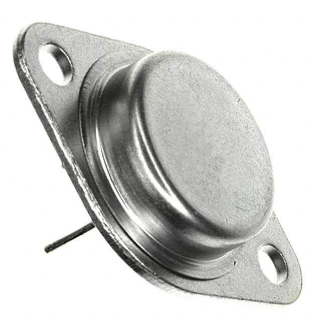
| 描述 | IC REG LDO 5V 0.1A TO92-3线性稳压器 0.1A Pos Volt Reg |
| 产品分类 | |
| 品牌 | Fairchild Semiconductor |
| 产品手册 | |
| 产品图片 |
|
| rohs | 符合RoHS无铅 / 符合限制有害物质指令(RoHS)规范要求 |
| 产品系列 | 电源管理 IC,线性稳压器,Fairchild Semiconductor LM78L05ACZ- |
| 数据手册 | |
| 产品型号 | LM78L05ACZ |
| PCN设计/规格 | |
| PSRR/纹波抑制—典型值 | 80 dB |
| 产品目录页面 | |
| 产品种类 | |
| 供应商器件封装 | TO-92-3 |
| 其它名称 | LM78L05ACZFS |
| 包装 | 散装 |
| 单位重量 | 179 mg |
| 商标 | Fairchild Semiconductor |
| 安装类型 | 通孔 |
| 安装风格 | Through Hole |
| 封装 | Bulk |
| 封装/外壳 | TO-226-3、TO-92-3 标准主体 |
| 封装/箱体 | TO-92 |
| 工作温度 | 0°C ~ 125°C |
| 工厂包装数量 | 1000 |
| 最大功率耗散 | 750 mW |
| 最大工作温度 | + 125 C |
| 最大输入电压 | 30 V |
| 最小工作温度 | 0 C |
| 最小输入电压 | 5.7 V |
| 极性 | Positive |
| 标准包装 | 1,000 |
| 电压-跌落(典型值) | 1.7V @ 40mA |
| 电压-输入 | 最高 30V |
| 电压-输出 | 5V |
| 电流-输出 | 100mA |
| 电流-限制(最小值) | - |
| 稳压器拓扑 | 正,固定式 |
| 稳压器数 | 1 |
| 系列 | LM78L05 |
| 线路调整率 | 150 mV |
| 负载调节 | 60 mV |
| 输出电压 | 5 V |
| 输出电流 | 0.1 A |
| 输出端数量 | 1 |
| 输出类型 | Fixed |
| 零件号别名 | LM78L05ACZ_NL |

,TO-226_straightlead.jpg)


- 商务部:美国ITC正式对集成电路等产品启动337调查
- 曝三星4nm工艺存在良率问题 高通将骁龙8 Gen1或转产台积电
- 太阳诱电将投资9.5亿元在常州建新厂生产MLCC 预计2023年完工
- 英特尔发布欧洲新工厂建设计划 深化IDM 2.0 战略
- 台积电先进制程称霸业界 有大客户加持明年业绩稳了
- 达到5530亿美元!SIA预计今年全球半导体销售额将创下新高
- 英特尔拟将自动驾驶子公司Mobileye上市 估值或超500亿美元
- 三星加码芯片和SET,合并消费电子和移动部门,撤换高东真等 CEO
- 三星电子宣布重大人事变动 还合并消费电子和移动部门
- 海关总署:前11个月进口集成电路产品价值2.52万亿元 增长14.8%


PDF Datasheet 数据手册内容提取
Is Now Part of To learn more about ON Semiconductor, please visit our website at www.onsemi.com Please note: As part of the Fairchild Semiconductor integration, some of the Fairchild orderable part numbers will need to change in order to meet ON Semiconductor’s system requirements. Since the ON Semiconductor product management systems do not have the ability to manage part nomenclature that utilizes an underscore (_), the underscore (_) in the Fairchild part numbers will be changed to a dash (-). This document may contain device numbers with an underscore (_). Please check the ON Semiconductor website to verify the updated device numbers. The most current and up-to-date ordering information can be found at www.onsemi.com. Please email any questions regarding the system integration to Fairchild_questions@onsemi.com. ON Semiconductor and the ON Semiconductor logo are trademarks of Semiconductor Components Industries, LLC dba ON Semiconductor or its subsidiaries in the United States and/or other countries. ON Semiconductor owns the rights to a number of patents, trademarks, copyrights, trade secrets, and other intellectual property. A listing of ON Semiconductor’s product/patent coverage may be accessed at www.onsemi.com/site/pdf/Patent-Marking.pdf. ON Semiconductor reserves the right to make changes without further notice to any products herein. ON Semiconductor makes no warranty, representation or guarantee regarding the suitability of its products for any particular purpose, nor does ON Semiconductor assume any liability arising out of the application or use of any product or circuit, and specifically disclaims any and all liability, including without limitation special, consequential or incidental damages. Buyer is responsible for its products and applications using ON Semiconductor products, including compliance with all laws, regulations and safety requirements or standards, regardless of any support or applications information provided by ON Semiconductor. “Typical” parameters which may be provided in ON Semiconductor data sheets and/or specifications can and do vary in different applications and actual performance may vary over time. All operating parameters, including “Typicals” must be validated for each customer application by customer’s technical experts. ON Semiconductor does not convey any license under its patent rights nor the rights of others. ON Semiconductor products are not designed, intended, or authorized for use as a critical component in life support systems or any FDA Class 3 medical devices or medical devices with a same or similar classification in a foreign jurisdiction or any devices intended for implantation in the human body. Should Buyer purchase or use ON Semiconductor products for any such unintended or unauthorized application, Buyer shall indemnify and hold ON Semiconductor and its officers, employees, subsidiaries, affiliates, and distributors harmless against all claims, costs, damages, and expenses, and reasonable attorney fees arising out of, directly or indirectly, any claim of personal injury or death associated with such unintended or unauthorized use, even if such claim alleges that ON Semiconductor was negligent regarding the design or manufacture of the part. ON Semiconductor is an Equal Opportunity/Affirmative Action Employer. This literature is subject to all applicable copyright laws and is not for resale in any manner.
M C 7 8 July 2015 L X X A / L M MC78LXXA / LM78LXXA 7 8 3-Terminal 0.1 A Positive Voltage Regulator L X X A — 3 Features Description -T e • Maximum Output Current of 100 mA The MC78LXXA / LM78LXXA series of fixed-voltage rm monolithic integrated circuit voltage regulators are suit- • Output Voltage of 5 V, 6 V, 8 V, 12 V, and 15 V able for applications that required supply current up to in • Thermal Overload Protection a 100 mA. l • Short-Circuit Current Limiting 0 . 1 • Output Voltage Offered in ±5% Tolerance TO-92 SOT-89 8-SOIC A P GND o s 8 1 it 1 2 3 iv 1. Output 2. GND e 123 3. GND 4. NC V o 1. Output 2. GND 3. Input 5. NC 6. GND l 7. GND 8. Input ta g e R e Ordering Information g u l a t Product Number Package Packing Method Output Voltage Tolerance Operating Temperature o r LM78L05ACZ Bulk LM78L05ACZX Tape & Reel LM78L05ACZXA Ammo LM78L12ACZ Bulk LM78L12ACZX Tape & Reel MC78L05ACP TO-92 Bulk MC78L05ACPXA Ammo MC78L06ACP Bulk ±5% -40 to +125°C MC78L08ACP Bulk MC78L15ACP Bulk MC78L15ACPXA Ammo MC78L05ACD Rail 8-SOIC MC78L05ACDX Tape & Reel MC78L05ACHX Tape & Reel SOT-89 MC78L08ACHX Tape & Reel © 2002 Fairchild Semiconductor Corporation www.fairchildsemi.com MC78LXXA / LM78LXXA Rev. 1.9
M C Block Diagram 7 8 L X X InpuVtI A 3 / L M THERMAL SHUTDOWN 7 I CIRCUIT 8 L X X A REFERENCE VOLTAGE + — - 3 - T e r SHORT- CIRCUIT m PROTECTION RSC i n a l 0 . GND VO0utput 1 2 1 A P o Figure 1. Block Diagram s i t i v e V Absolute Maximum Ratings o l t Stresses exceeding the absolute maximum ratings may damage the device. The device may not function or be opera- a g ble above the recommended operating conditions and stressing the parts to these levels is not recommended. In addi- e tion, extended exposure to stresses above the recommended operating conditions may affect device reliability. The R absolute maximum ratings are stress ratings only. Values are at T = 25°C unless otherwise noted. e A g u Symbol Parameter Value Unit l a t V = 5 V to 8 V 30 V o V Input Voltage O r I V = 12 V to 15 V 35 V O T Operating Temperature Range -40 to +125°C °C OPR T Maximum Junction Temperature 150 °C J(MAX) T Storage Temperature Range -65 to +150 °C STG RθJC Thermal Resistance, Junction-Case TO-92 50 °C/W TO-92 150 °C/W RθJA Thermal Resistance, Junction-Air SOT-89 225 °C/W 8-SOIC 160 °C/W © 2002 Fairchild Semiconductor Corporation www.fairchildsemi.com MC78LXXA / LM78LXXA Rev. 1.9 2
M C Electrical Characteristics (MC78L05A / LM78L05A) 7 8 V = 10 V, I = 40 mA, -40°C ≤ T ≤ 125°C, C = 0.33 μF, C = 0.1 μF, unless otherwise specified. L I O J I O X X Symbol Parameter Conditions Min. Typ. Max. Unit A VO Output Voltage TJ = 25°C 4.8 5.0 5.2 V / L 7 V ≤ V ≤ 20 V 8 150 mV M ΔV Line Regulation(1) T = 25°C I 7 O J 8 V ≤ V ≤ 20 V 6 100 mV 8 I L 1 mA ≤ I ≤ 100 mA 11 60 mV X ΔV Load Regulation(1) T = 25°C O X O J 1 mA ≤ I ≤ 40 mA 5.0 30.0 mV A O 7 V ≤ V ≤ 20 V 1 mA ≤ I ≤ 40 mA 5.25 V — I O VO Output Voltage 7 V ≤ VI ≤ VMAX(2) 1 mA ≤ IO ≤ 70 mA 4.75 5.25 V 3-T I Quiescent Current T = 25°C 2.0 5.5 mA e Q J r m ΔIQ Quiescent Current With Line 8 V ≤ VI ≤ 20 V 1.5 mA i n ΔI Change With Load 1 mA ≤ I ≤ 40 mA 0.1 mA a Q O l V Output Noise Voltage T = 25°C, 10 Hz ≤ f ≤ 100 kHz 40 μV/Vo 0 N A . 1 ΔV /ΔT Temperature Coefficient of V I = 5 mA -0.65 mV/°C O O O A RR Ripple Rejection f = 120 Hz, 8 V ≤ V ≤ 18 V, T = 25°C 41 80 dB P I J o VD Dropout Voltage TJ = 25°C 1.7 V s i t i Notes: v e 1. The maximum steady-state usable output current and input voltage are very dependent on the heat sinking and/or V lead length of the package. The data above represents pulse test conditions with junction temperature as indicated o at the initiation of tests. l t 2. Power dissipation P ≤ 0.75 W. a D g e R e g u l a t o r © 2002 Fairchild Semiconductor Corporation www.fairchildsemi.com MC78LXXA / LM78LXXA Rev. 1.9 3
M C Electrical Characteristics (MC78L06A) 7 8 V = 12 V, I = 40 mA, -40°C ≤ T ≤ 125°C, C = 0.33 μF, C = 0.1 μF, unless otherwise specified. L I O J I O X X Symbol Parameter Conditions Min. Typ. Max. Unit A VO Output Voltage TJ = 25°C 5.75 6.0 6.25 V / L 8.5 V ≤ V ≤ 20 V 64 175 mV M ΔV Line Regulation(3) T = 25°C I 7 O J 9 V ≤ V ≤ 20 V 54 125 mV 8 I L 1 mA ≤ I ≤ 100 mA 12.8 80.0 mV X ΔV Load Regulation(3) T = 25°C O X O J 1 mA ≤ I ≤ 70 mA 5.8 40.0 mV A O 8.5 V ≤ V ≤ 20 V, 1 mA ≤ I ≤ 40 mA 5.7 6.3 V — I O VO Output Voltage 8.5 V ≤ VI ≤ VMAX(4), 1 mA ≤ IO ≤ 70 mA 5.7 6.3 V 3-T T = 25°C 5.5 mA e J r IQ Quiescent Current T = 125°C 3.9 6.0 mA m J i n ΔIQ Quiescent Current With Line 9 V ≤ VI ≤ 20 V 1.5 mA a l ΔI Change With Load 1 mA ≤ I ≤ 40 mA 0.1 mA 0 Q O . 1 V Output Noise Voltage T = 25°C, 10 Hz ≤ f ≤ 100 kHz 40 μV/Vo N A A ΔV /ΔT Temperature Coefficient of V I = 5 mA 0.75 mV/°C P O O O o RR Ripple Rejection f = 120 Hz, 10 V ≤ VI ≤ 20 V, TJ = 25°C 40 46 dB s i V Dropout Voltage T = 25°C 1.7 V ti D J v e Notes: V 3. The maximum steady-state usable output current and input voltage are very dependent on the heat sinking o l and/or lead length of the package. The data above represents pulse test conditions with junction temperature ta as indicated at the initiation of tests. g 4. Power dissipation PD ≤ 0.75 W. e R e g u l a t o r © 2002 Fairchild Semiconductor Corporation www.fairchildsemi.com MC78LXXA / LM78LXXA Rev. 1.9 4
M C Electrical Characteristics (MC78L08A) 7 8 V = 14 V, I = 40 mA, -40°C ≤ T ≤ 125°C, C = 0.33 μF, C = 0.1 μF, unless otherwise specified. L I O J I O X X Symbol Parameter Conditions Min. Typ. Max. Unit A VO Output Voltage TJ = 25°C 7.7 8.0 8.3 V / L 10.5 V ≤ V ≤ 23 V 10 175 mV M ΔV Line Regulation(5) T = 25°C I 7 O J 11 V ≤ V ≤ 23 V 8 125 mV 8 I L 1 mA ≤ I ≤ 100 mA 15 80 mV X ΔV Load Regulation(5) T = 25°C O X O J 1 mA ≤ I ≤ 40 mA 8 40 mV A O 10.5V ≤ V≤ 23V 1 mA ≤ I ≤ 40 mA 7.6 8.4 V — I O VO Output Voltage 10.5V ≤ VI ≤ VMAX(6) 1 mA ≤ IO ≤ 70 mA 7.6 8.4 V 3-T I Quiescent Current T = 25°C 2.0 5.5 mA e Q J r m ΔIQ Quiescent Current With Line 11 V ≤ VI ≤ 23 V 1.5 mA i n ΔI Change With Load 1 mA ≤ I ≤ 40 mA 0.1 mA a Q O l V Output Noise Voltage T = 25°C, 10 Hz ≤ f ≤100 kHz 60 μV/Vo 0 N A . 1 ΔV /ΔT Temperature Coefficient of V I = 5 mA -0.8 mV/°C O O O A RR Ripple Rejection f = 120 Hz, 11 V ≤ V ≤ 21 V, T = 25°C 39 70 dB P I J o VD Dropout Voltage TJ = 25°C 1.7 V s i t i Notes: v e 5. The maximum steady-state usable output current and input voltage are very dependent on the heat sinking and/or V lead length of the package. The data above represents pulse test conditions with junction temperature as indicated o at the initiation of tests. l t 6. Power dissipation P ≤ 0.75 W. a D g e R e g u l a t o r © 2002 Fairchild Semiconductor Corporation www.fairchildsemi.com MC78LXXA / LM78LXXA Rev. 1.9 5
M C Electrical Characteristics (MC78L12A / LM78L12A) 7 8 V = 19 V, I = 40 mA, -40°C ≤ T ≤ 125°C, C = 0.33 μF, C = 0.1 μF, unless otherwise specified. L I O J I O X X Symbol Parameter Conditions Min. Typ. Max. Unit A VO Output Voltage TJ = 25°C 11.5 12.0 12.5 V / L 14.5 V ≤ V ≤ 27 V 20 250 mV M ΔV Line Regulation (7) T = 25°C I 7 O J 16 V ≤ V ≤ 27 V 15 200 mV 8 I L 1 mA ≤ I ≤ 100 mA 20 100 mV X ΔV Load Regulation (7) T = 25°C O X O J 1 mA ≤ I ≤ 40 mA 10 50 mV A O 14.5 V ≤ V≤ 27 V 1 mA ≤ I ≤ 40 mA 11.4 12.6 V — I O VO Output Voltage 14.5 V ≤ VI ≤ VMAX(8) 1 mA ≤ IO ≤ 70 mA 11.4 12.6 V 3-T I Quiescent Current T = 25°C 2.1 6.0 mA e Q J r m ΔIQ Quiescent With Line 16 V ≤ VI ≤ 27 V 1.5 mA i n ΔI Current Change With Load 1 mA ≤ I ≤ 40 mA 0.1 mA a Q O l V Output Noise Voltage T = 25°C, 10 Hz ≤ f ≤ 100 kHz 80 μV/Vo 0 N A . 1 ΔV /ΔT Temperature Coefficient of V I = 5 mA -1.0 mV/°C O O O A RR Ripple Rejection f = 120 Hz, 15 V ≤ V ≤ 25 V, T = 25°C 37 65 dB P I J o VD Dropout Voltage TJ = 25°C 1.7 V s i t i Notes: v e 7. The maximum steady-state usable output current and input voltage are very dependent on the heat sinking and/or V lead length of the package. The data above represents pulse test conditions with junction temperature as indicated o at the initiation of tests. l t 8. Power dissipation P ≤ 0.75 W. a D g e R e g u l a t o r © 2002 Fairchild Semiconductor Corporation www.fairchildsemi.com MC78LXXA / LM78LXXA Rev. 1.9 6
M C Electrical Characteristics (MC78L15A) 7 8 V = 23 V, I = 40 mA, -40°C ≤ T ≤ 125°C, C = 0.33 μF, C = 0.1 μF, unless otherwise specified. L I O J I O X X Symbol Parameter Conditions Min. Typ. Max. Unit A VO Output Voltage TJ = 25°C 14.4 15.0 15.6 V / L 17.5 V ≤ V ≤ 30 V 25 300 mV M ΔV Line Regulation(9) T = 25°C I 7 O J 20 V ≤ V ≤ 30 V 20 250 mV 8 I L 1 mA ≤ I ≤ 100 mA 25 150 mV X ΔV Load Regulation(9) T = 25°C O X O J 1 mA ≤ I ≤ 40 mA 12 75 mV A O 17.5 V ≤ V≤ 30 V 1 mA ≤ I ≤ 40 mA 14.25 15.75 V — I O VO Output Voltage 17.5 V ≤ VI ≤ VMAX(10) 1 mA ≤ IO ≤ 70 mA 14.25 15.75 V 3-T I Quiescent Current T = 25°C 2.1 6.0 mA e Q J r m ΔIQ Quiescent With Line 20 V ≤ VI ≤ 30 V 1.5 mA i n ΔI Current Change With Load 1 mA ≤ I ≤ 40 mA 0.1 mA a Q O l V Output Noise Voltage T = 25°C, 10 Hz ≤ f ≤ 100 kHz 90 μV/Vo 0 N A . 1 ΔV /ΔT Temperature Coefficient of V I = 5 mA -1.3 mV/°C O O O A RR Ripple Rejection f = 120 Hz, 18.5 V ≤ V ≤28.5 V, T = 25°C 34 60 dB P I J o VD Dropout Voltage TJ = 25°C 1.7 V s i t i Notes: v e 9. The maximum steady-state usable output current and input voltage are very dependent on the heat sinking and/or V lead length of the package. The data above represents pulse test conditions with junction temperature as indicated o l at the initiation of tests. ta 10. Power dissipation P ≤ 0.75 W. g D e R e g u l a t o r © 2002 Fairchild Semiconductor Corporation www.fairchildsemi.com MC78LXXA / LM78LXXA Rev. 1.9 7
M C Typical Application 7 8 L X X A INPUT 3(8) MC78MLKCX7XA8AL7X /8X LALM/LXM7X87L8ALXXXXAA(13) 1(1) OUTPUT / L NOTE 1 M C0C.1I3(134)μF 2(2,3,6,7) C0.O (114μ)F 78L NOTE 2 NOTE 2 X X A — 3 - T e r m Figure 2. Typical Application i n a Notes: l 0 13. To specify an output voltage, substitute voltage value for “XX”. . 1 14.CI is required if the regulator is located an appreciable distance from the power supply filter. Though Co is not A needed for stability, it improves transient response. Bypass capacitors are recommended for optimum stability and P transient response and should be located as close as possible to the regulator. o s i t i v e V o l t a g e R e g u l a t o r © 2002 Fairchild Semiconductor Corporation www.fairchildsemi.com MC78LXXA / LM78LXXA Rev. 1.9 8
None
None
None
4.70 C A 4.30 2.23MIN 1.87 0.30 X 45° 0.50 X 45° C 1.45 B 1.40 CL SYMM 2.70 C 5.30MIN 90° 4.50 2.30 C 3.90 1.30 1 2 3 0.89 2.00MIN 0.52 (2X) C 0.30 0.54 1 2 3 0.10 M C A B 1.50 3.00 0.90MIN 2X 0.96MIN 1.70 1.50 C 1.30 3.00MIN LAND PATTERN RECOMMENDATION SEATING PLANE C 0.60 C 0.40 0.50 0.35 0.35 3 1 2.29 2.70 2.13 NOTES: UNLESS OTHERWISE SPECIFIED. A. REFERENCE TO JEDEC TO-243 VARIATION AA. B. ALL DIMENSIONS ARE IN MILLIMETERS. C DOES NOT COMPLY JEDEC STANDARD VALUE. D. DIMENSIONS ARE EXCLUSIVE OF BURRS, MOLD FLASH AND TIE BAR PROTRUSION. E. DIMENSION AND TOLERANCE AS PER ASME Y14.5-1994. F. DRAWING FILE NAME: MA03CREV3
ON Semiconductor and are trademarks of Semiconductor Components Industries, LLC dba ON Semiconductor or its subsidiaries in the United States and/or other countries. ON Semiconductor owns the rights to a number of patents, trademarks, copyrights, trade secrets, and other intellectual property. A listing of ON Semiconductor’s product/patent coverage may be accessed at www.onsemi.com/site/pdf/Patent−Marking.pdf. ON Semiconductor reserves the right to make changes without further notice to any products herein. ON Semiconductor makes no warranty, representation or guarantee regarding the suitability of its products for any particular purpose, nor does ON Semiconductor assume any liability arising out of the application or use of any product or circuit, and specifically disclaims any and all liability, including without limitation special, consequential or incidental damages. Buyer is responsible for its products and applications using ON Semiconductor products, including compliance with all laws, regulations and safety requirements or standards, regardless of any support or applications information provided by ON Semiconductor. “Typical” parameters which may be provided in ON Semiconductor data sheets and/or specifications can and do vary in different applications and actual performance may vary over time. All operating parameters, including “Typicals” must be validated for each customer application by customer’s technical experts. ON Semiconductor does not convey any license under its patent rights nor the rights of others. ON Semiconductor products are not designed, intended, or authorized for use as a critical component in life support systems or any FDA Class 3 medical devices or medical devices with a same or similar classification in a foreign jurisdiction or any devices intended for implantation in the human body. Should Buyer purchase or use ON Semiconductor products for any such unintended or unauthorized application, Buyer shall indemnify and hold ON Semiconductor and its officers, employees, subsidiaries, affiliates, and distributors harmless against all claims, costs, damages, and expenses, and reasonable attorney fees arising out of, directly or indirectly, any claim of personal injury or death associated with such unintended or unauthorized use, even if such claim alleges that ON Semiconductor was negligent regarding the design or manufacture of the part. ON Semiconductor is an Equal Opportunity/Affirmative Action Employer. This literature is subject to all applicable copyright laws and is not for resale in any manner. PUBLICATION ORDERING INFORMATION LITERATURE FULFILLMENT: N. American Technical Support: 800−282−9855 Toll Free ON Semiconductor Website: www.onsemi.com Literature Distribution Center for ON Semiconductor USA/Canada 19521 E. 32nd Pkwy, Aurora, Colorado 80011 USA Europe, Middle East and Africa Technical Support: Order Literature: http://www.onsemi.com/orderlit Phone: 303−675−2175 or 800−344−3860 Toll Free USA/Canada Phone: 421 33 790 2910 Fax: 303−675−2176 or 800−344−3867 Toll Free USA/Canada Japan Customer Focus Center For additional information, please contact your local Email: orderlit@onsemi.com Phone: 81−3−5817−1050 Sales Representative © Semiconductor Components Industries, LLC www.onsemi.com www.onsemi.com 1
Mouser Electronics Authorized Distributor Click to View Pricing, Inventory, Delivery & Lifecycle Information: O N Semiconductor: LM78L05ACZ LM78L05ACZXA LM78L05ACZX