ICGOO在线商城 > 传感器,变送器 > 温度传感器 - 模拟和数字输出 > LM61CIM3/NOPB

 Datasheet下载
- 型号: LM61CIM3/NOPB
- 制造商: Texas Instruments
- 库位|库存: xxxx|xxxx
- 要求:
| 数量阶梯 | 香港交货 | 国内含税 |
| +xxxx | $xxxx | ¥xxxx |
查看当月历史价格
查看今年历史价格
LM61CIM3/NOPB产品简介:
ICGOO电子元器件商城为您提供LM61CIM3/NOPB由Texas Instruments设计生产,在icgoo商城现货销售,并且可以通过原厂、代理商等渠道进行代购。 LM61CIM3/NOPB价格参考。Texas InstrumentsLM61CIM3/NOPB封装/规格:温度传感器 - 模拟和数字输出, Temperature Sensor Analog, Local -30°C ~ 100°C 10mV/°C SOT-23-3。您可以下载LM61CIM3/NOPB参考资料、Datasheet数据手册功能说明书,资料中有LM61CIM3/NOPB 详细功能的应用电路图电压和使用方法及教程。
LM61CIM3/NOPB是德州仪器(Texas Instruments)生产的一款模拟输出型温度传感器,属于LM61系列。该器件具有单电源供电、低功耗和高精度的特点,输出电压与摄氏温度呈线性关系,无需外部校准即可实现较宽温度范围内的准确测温。

典型应用场景包括:

1. 消费类电子产品:广泛用于手机、平板电脑、笔记本电脑等设备中,监测系统内部温度,防止过热,保障设备稳定运行。

2. 工业控制:适用于工业自动化设备、PLC模块、电机驱动器等环境,用于实时监控设备工作温度,提升系统安全性和可靠性。

3. 电源管理系统:在开关电源、DC-DC转换器、电池充电管理模块中,用于温度补偿和过温保护,优化电源效率并防止热损坏。

4. 医疗设备:应用于便携式医疗仪器(如体温计、监护仪)中,提供稳定的温度检测功能,确保设备在安全温度范围内工作。

5. 汽车电子:用于车载信息娱乐系统、车身控制模块等非引擎舱区域的温度监测,适应较宽的工作温度范围(-40°C 至 +125°C)。

6. 家用电器:如空调、冰箱、洗衣机等智能家电中的温度感知单元,实现智能化温控管理。

LM61CIM3/NOPB采用SOT-23小尺寸封装,便于在空间受限的电路板上布局,适合对成本和空间敏感的应用。其模拟输出接口简单,可直接连接MCU的ADC引脚,无需复杂通信协议,设计便捷,是中低温范围内经济可靠的温度传感解决方案。
| 参数 | 数值 |
| 产品目录 | |
| 描述 | IC TEMPERATURE SENSOR SOT23-3板上安装温度传感器 Ana Output Temp Sens |
| 产品分类 | 温度传感器,变送器温度传感器 |
| 品牌 | Texas Instruments |
| 产品手册 | |
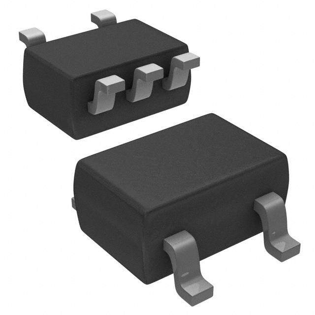
| 产品图片 |
|
| rohs | 符合RoHS无铅 / 符合限制有害物质指令(RoHS)规范要求 |
| 产品系列 | 板上安装温度传感器,Texas Instruments LM61CIM3/NOPB- |
| 数据手册 | |
| 产品型号 | LM61CIM3/NOPB |
| 产品目录页面 | |
| 产品种类 | 板上安装温度传感器 |
| 供应商器件封装 | SOT-23-3 |
| 关闭 | Shutdown |
| 其它名称 | LM61CIM3/NOPBDKR |
| 准确性 | +/- 4 C |
| 制造商产品页 | http://www.ti.com/general/docs/suppproductinfo.tsp?distId=10&orderablePartNumber=LM61CIM3/NOPB |
| 包装 | Digi-Reel® |
| 商标 | Texas Instruments |
| 增益 | 10 mV / C |
| 安装风格 | SMD/SMT |
| 封装 | Reel |
| 封装/外壳 | TO-236-3,SC-59,SOT-23-3 |
| 封装/箱体 | SOT-23-3 |
| 工厂包装数量 | 1000 |
| 感应温度 | -30°C ~ 100°C |
| 数字输出-位数 | None |
| 数字输出-总线接口 | - |
| 最大工作温度 | + 100 C |
| 最小工作温度 | - 30 C |
| 标准包装 | 1 |
| 电压-电源 | 2.7 V ~ 10 V |
| 电源电压-最大 | 10 V |
| 电源电压-最小 | 2.7 V |
| 电源电流 | 155 uA |
| 精度 | ±4% |
| 系列 | LM61 |
| 设备功能 | Sensor |
| 输出电流 | 10 mA |
| 输出类型 | Analog |
| 配置 | Local |


- 商务部:美国ITC正式对集成电路等产品启动337调查
- 曝三星4nm工艺存在良率问题 高通将骁龙8 Gen1或转产台积电
- 太阳诱电将投资9.5亿元在常州建新厂生产MLCC 预计2023年完工
- 英特尔发布欧洲新工厂建设计划 深化IDM 2.0 战略
- 台积电先进制程称霸业界 有大客户加持明年业绩稳了
- 达到5530亿美元!SIA预计今年全球半导体销售额将创下新高
- 英特尔拟将自动驾驶子公司Mobileye上市 估值或超500亿美元
- 三星加码芯片和SET,合并消费电子和移动部门,撤换高东真等 CEO
- 三星电子宣布重大人事变动 还合并消费电子和移动部门
- 海关总署:前11个月进口集成电路产品价值2.52万亿元 增长14.8%


PDF Datasheet 数据手册内容提取
Product Sample & Technical Tools & Support & Folder Buy Documents Software Community LM61 SNIS121J–JUNE1999–REVISEDNOVEMBER2016 LM61 2.7-V, SOT-23 or TO-92 Temperature Sensor 1 Features 3 Description • CalibratedLinearScaleFactorof10mV/°C The LM61 device is a precision, integrated-circuit 1 temperature sensor that can sense a –30°C to 100°C • RatedforFullTemperatureRange(–30° to temperature range while operating from a single 100°C) 2.7‑V supply. The output voltage of the LM61 is • SuitableforRemoteApplications linearly proportional to temperature (10 mV/°C) and • ULRecognizedComponent has a DC offset of 600 mV. The offset allows reading negative temperatures without the need for a • ±2°Cor±3°CAccuracyat25°C(Maximum) negative supply. The nominal output voltage of the • ±3°CAccuracyfor –25°Cto85°C(Maximum) LM61rangesfrom300mVto1600mVfora–30°Cto • ±4°CAccuracyfor –30°Cto100°C(Maximum) 100°C temperature range. The LM61 is calibrated to provide accuracies of ±2°C at room temperature and • 10mV/°CTemperatureSlope(Maximum) ±3°Coverthefull –25°Cto85°Ctemperaturerange. • 2.7-Vto10-VPowerSupplyVoltageRange The linear output of the LM61, 600-mV offset, and • 125-µACurrentDrainat25°C(Maximum) factory calibration simplify external circuitry required • ±0.8°CNonlinearity(Maximum) in a single supply environment where reading • 800-ΩOutputImpedance(Maximum) negative temperatures is required. Because the quiescent current is less than 125 µA, self-heating is 2 Applications limited to a very low 0.2°C in still air. Shutdown capability for the LM61 is intrinsic because its • CellularPhones inherent low power consumption allows it to be • Computers powereddirectlyfromtheoutputofmanylogicgates. • PowerSupplyModules DeviceInformation(1) • BatteryManagement PARTNUMBER PACKAGE BODYSIZE(NOM) • FAXMachines SOT-23(3) 1.30mm×2.92mm • Printers LM61 TO-92(3) 4.30mm×4.30mm • HVAC (1) For all available packages, see the orderable addendum at • DiskDrives theendofthedatasheet. • Appliances KeySpecifications TypicalApplication VALUE Accuracyat25°C ±2°Cor±3°C Accuracyfor–25°Cto85°C ±3°C Accuracyfor–30°Cto100°C ±4°C Temperatureslope 10mV/°C Powersupplyvoltage 2.7Vto10V Currentdrainat25°C 125µA Nonlinearity ±0.8°C Outputimpedance 800Ω V =(10mV/°C×T°C)+600mV O 1 An IMPORTANT NOTICE at the end of this data sheet addresses availability, warranty, changes, use in safety-critical applications, intellectualpropertymattersandotherimportantdisclaimers.PRODUCTIONDATA.
LM61 SNIS121J–JUNE1999–REVISEDNOVEMBER2016 www.ti.com Table of Contents 1 Features.................................................................. 1 8 ApplicationandImplementation.......................... 8 2 Applications........................................................... 1 8.1 ApplicationInformation..............................................8 3 Description............................................................. 1 8.2 TypicalApplications..................................................8 4 RevisionHistory..................................................... 2 9 PowerSupplyRecommendations...................... 11 5 PinConfigurationandFunctions......................... 3 10 Layout................................................................... 11 6 Specifications......................................................... 3 10.1 LayoutGuidelines.................................................11 6.1 AbsoluteMaximumRatings......................................3 10.2 LayoutExamples...................................................11 6.2 ESDRatings..............................................................3 10.3 ThermalConsiderations........................................12 6.3 RecommendedOperatingConditions.......................3 11 DeviceandDocumentationSupport................. 14 6.4 ThermalInformation..................................................4 11.1 RelatedDocumentation.........................................14 6.5 ElectricalCharacteristics...........................................4 11.2 ReceivingNotificationofDocumentationUpdates14 6.6 TypicalCharacteristics..............................................5 11.3 CommunityResources..........................................14 7 DetailedDescription.............................................. 7 11.4 Trademarks...........................................................14 7.1 Overview...................................................................7 11.5 ElectrostaticDischargeCaution............................14 7.2 FunctionalBlockDiagram.........................................7 11.6 Glossary................................................................14 7.3 FeatureDescription...................................................7 12 Mechanical,Packaging,andOrderable Information........................................................... 14 7.4 DeviceFunctionalModes..........................................7 4 Revision History NOTE:Pagenumbersforpreviousrevisionsmaydifferfrompagenumbersinthecurrentversion. ChangesfromRevisionI(February2013)toRevisionJ Page • AddedDeviceInformationtable,DeviceComparisonTable,PinConfigurationandFunctionssection,Specifications section,ESDRatingstable,DetailedDescriptionsection,ApplicationandImplementationsection,PowerSupply Recommendationssection,Layoutsection,DeviceandDocumentationSupportsection,andMechanical, Packaging,andOrderableInformationsection...................................................................................................................... 1 • AddedThermalInformationtable........................................................................................................................................... 4 • ChangedR valuesforDBZ(SOT-23)From:450°C/WTo:286.3°C/WandforLP(TO-92)From:180°C/WTo: θJA 162.2°C/W.............................................................................................................................................................................. 4 ChangesfromRevisionH(February2013)toRevisionI Page • ChangedlayoutofNationalSemiconductorDataSheettoTIformat.................................................................................... 1 2 SubmitDocumentationFeedback Copyright©1999–2016,TexasInstrumentsIncorporated ProductFolderLinks:LM61
LM61 www.ti.com SNIS121J–JUNE1999–REVISEDNOVEMBER2016 5 Pin Configuration and Functions DBZPackage LPPackage 3-PinSOT-23 3-PinTO-92 TopView PinFunctions PIN TYPE DESCRIPTION NAME NO. +VS 1 Power Positivepowersupplypin. VOUT 2 Output Temperaturesensoranalogoutput. GND 3 Ground Devicegroundpin,connectedtopowersupplynegativeterminal. 6 Specifications 6.1 Absolute Maximum Ratings overoperatingfree-airtemperaturerange(unlessotherwisenoted)(1) MIN MAX UNIT Supplyvoltage 12 –0.2 V Outputvoltage (+V +0.6) –0.6 V S Outputcurrent 10 mA Inputcurrentatanypin(2) 5 mA Maximumjunctiontemperature,T 125 °C J Storagetemperature,T –65 150 °C stg (1) StressesbeyondthoselistedunderAbsoluteMaximumRatingsmaycausepermanentdamagetothedevice.Thesearestressratings only,whichdonotimplyfunctionaloperationofthedeviceattheseoranyotherconditionsbeyondthoseindicatedunderRecommended OperatingConditions.Exposuretoabsolute-maximum-ratedconditionsforextendedperiodsmayaffectdevicereliability. (2) Whentheinputvoltage(V)atanypinexceedspowersupplies(V <GNDorV >V ),thecurrentatthatpinmustbelimitedto5mA. I I I S 6.2 ESD Ratings VALUE UNIT Human-bodymodel(HBM),perANSI/ESDA/JEDECJS-001(1)(2) ±2500 V Electrostaticdischarge V (ESD) MachineModel(MM)(3) ±250 (1) JEDECdocumentJEP155statesthat500-VHBMallowssafemanufacturingwithastandardESDcontrolprocess. (2) Thehumanbodymodelisa100-pFcapacitordischargedthrougha1.5-kΩresistorintoeachpin. (3) Themachinemodelisa200-pFcapacitordischargeddirectlyintoeachpin. 6.3 Recommended Operating Conditions MIN MAX UNIT +V Supplyvoltage 2 10 V S LM61C –30 100 T Operatingtemperature °C LM61B –25 85 Copyright©1999–2016,TexasInstrumentsIncorporated SubmitDocumentationFeedback 3 ProductFolderLinks:LM61
LM61 SNIS121J–JUNE1999–REVISEDNOVEMBER2016 www.ti.com 6.4 Thermal Information LM61 THERMALMETRIC(1) DBZ(SOT-23) LP(TO-92) UNIT 3PINS 3PINS R Junction-to-ambientthermalresistance(2) 286.3 162.2 °C/W θJA R Junction-to-case(top)thermalresistance 96 85 °C/W θJC(top) R Junction-to-boardthermalresistance 57.1 — °C/W θJB ψ Junction-to-topcharacterizationparameter 5.3 29.2 °C/W JT ψ Junction-to-boardcharacterizationparameter 55.8 141.4 °C/W JB (1) Formoreinformationabouttraditionalandnewthermalmetrics,seetheSemiconductorandICPackageThermalMetricsapplication report. (2) Thejunction-to-ambientthermalresistanceisspecifiedwithoutaheatsinkinstillair. 6.5 Electrical Characteristics +V =3V(DC)(1)(2) S PARAMETER TESTCONDITIONS MIN(3) TYP(4) MAX(3) UNIT LM61B –2 2 T =25°C A LM61C –3 3 Accuracy(5) °C LM61B –3 3 LM61C –4 4 Outputvoltageat0°C 600 mV LM61B –0.6 0.6 Nonlinearity(6) °C LM61C –0.8 0.8 LM61B 9.7 10 10.3 Sensorgain(averageslope) mV/°C LM61C 9.6 10 10.4 +V =3Vto10V 0.8 S Outputimpedance T =–30°Cto85°C,+V =2.7V 2.3 kΩ A S T =85°Cto100°C,+V =2.7V 5 A S +V =3Vto10V –0.7 0.7 mV/V Lineregulation(7) S +V =2.7Vto3.3V –5.7 5.7 mV S T =25°C 82 125 A Quiescentcurrent +V =2.7Vto10V µA S 155 Changeofquiescentcurrent +V =2.7Vto10V ±5 µA S Temperaturecoefficientofquiescentcurrent 0.2 µA/°C Longtermstability(8) T =T =100°C,for1000hours ±0.2 °C J MAX (1) LimitsarespecifiedtoTI'sAOQL(AverageOutgoingQualityLevel). (2) Typicallimitsrepresentmostlikelyparametricnorm. (3) MaximumandminimumlimitsapplyforT =T =T toT . A J MIN MAX (4) TypicallimitsapplyforT =T =25°C. A J (5) Accuracyisdefinedastheerrorbetweentheoutputvoltageand10mV/°Cmultipliedbythedevice'scasetemperatureplus600mV,at specifiedconditionsofvoltage,current,andtemperature(expressedin°C). (6) Nonlinearityisdefinedasthedeviationoftheoutput-voltage-versus-temperaturecurvefromthebest-fitstraightline,overthedevice's ratedtemperaturerange. (7) Regulationismeasuredatconstantjunctiontemperature,usingpulsetestingwithalowdutycycle.Changesinoutputduetoheating effectscanbecomputedbymultiplyingtheinternaldissipationbythethermalresistance. (8) Forbestlong-termstability,anyprecisioncircuitgivesbestresultsiftheunitisagedatawarmtemperature,ortemperaturecycledforat least46hoursbeforelong-termlifetestbegins.Thisisespeciallytruewhenasmall(Surface-Mount)partiswave-soldered;allowtime forstressrelaxationtooccur.Themajorityofthedriftoccursinthefirst1000hoursatelevatedtemperatures.Thedriftafter1000hours doesnotcontinueatthefirst1000-hourrate. 4 SubmitDocumentationFeedback Copyright©1999–2016,TexasInstrumentsIncorporated ProductFolderLinks:LM61
LM61 www.ti.com SNIS121J–JUNE1999–REVISEDNOVEMBER2016 6.6 Typical Characteristics TheLM61intheSOT-23packagemountedtoaprinted-circuitboardasshowninFigure18wasusedtogeneratethe followingthermalcurves. Figure1.Junction-to-AmbientThermalResistance Figure2.ThermalTimeConstant Figure3.ThermalResponseinStillAirwithHeatSink Figure4.ThermalResponseinStirredOilBath withHeatSink Figure5.ThermalResponseinStillAirwithoutHeatSink Figure6.QuiescentCurrentvsTemperature Copyright©1999–2016,TexasInstrumentsIncorporated SubmitDocumentationFeedback 5 ProductFolderLinks:LM61
LM61 SNIS121J–JUNE1999–REVISEDNOVEMBER2016 www.ti.com Typical Characteristics (continued) TheLM61intheSOT-23packagemountedtoaprinted-circuitboardasshowninFigure18wasusedtogeneratethe followingthermalcurves. Figure7.AccuracyvsTemperature Figure8.NoiseVoltage 2 V/Div +VS 0 V 0.2 V/Div V O 0 V 5 µs/Div Figure9.SupplyVoltagevsSupplyCurrent Figure10.Start-UpResponse 6 SubmitDocumentationFeedback Copyright©1999–2016,TexasInstrumentsIncorporated ProductFolderLinks:LM61
LM61 www.ti.com SNIS121J–JUNE1999–REVISEDNOVEMBER2016 7 Detailed Description 7.1 Overview The LM61 is a precision integrated-circuit temperature sensor that can sense a –30°C to 100°C temperature range using a single positive supply. The output voltage of the LM61 has a positive temperature slope of 10 mV/°C. A 600-mV offset is included, enabling negative temperature sensing when biased by a single supply. The temperature-sensing element is comprised of a delta-VBE architecture. The temperature-sensing element is then buffered by an amplifier and provided to the VOUT pin. The amplifier has a simple class A output stage as showninFunctionalBlockDiagram. 7.2 Functional Block Diagram 7.3 Feature Description 7.3.1 LM61TransferFunction The LM61 follows a simple linear transfer function to achieve the accuracy as listed in Electrical Characteristics. UseEquation1tocalculatethevalueofV . O V =10mV/°C×T°C+600mV O where • Tisthetemperaturein°C • V istheLM61outputvoltage (1) O 7.4 Device Functional Modes TheonlyfunctionalmodeoftheLM61deviceisananalogoutputdirectlyproportionaltotemperature. Copyright©1999–2016,TexasInstrumentsIncorporated SubmitDocumentationFeedback 7 ProductFolderLinks:LM61
LM61 SNIS121J–JUNE1999–REVISEDNOVEMBER2016 www.ti.com 8 Application and Implementation NOTE Information in the following applications sections is not part of the TI component specification, and TI does not warrant its accuracy or completeness. TI’s customers are responsible for determining suitability of components for their purposes. Customers should validateandtesttheirdesignimplementationtoconfirmsystemfunctionality. 8.1 Application Information The LM61 has a wide supply range and a 10-mV/°C output slope with a 600-mV DC. Therefore, it can be easily applied in many temperature-sensing applications where a single supply is required for positive and negative temperatures. 8.2 Typical Applications 8.2.1 TypicalTemperatureSensingCircuit V =10mV/°C×T°C+600mV O Figure11. TypicalTemperatureSensingCircuitDiagram 8.2.1.1 DesignRequirements Forthisdesignexample,usetheparameterslistedinTable1astheinputparameters. Table1.DesignParameters PARAMETER VALUE Powersupplyvoltage 2.7Vto3.3V Accuracyat25°C ±2°C(maximum) Accuracyover–25°Cto85°C ±3°C(maximum) Temperatureslope 10mV/°C 8 SubmitDocumentationFeedback Copyright©1999–2016,TexasInstrumentsIncorporated ProductFolderLinks:LM61
LM61 www.ti.com SNIS121J–JUNE1999–REVISEDNOVEMBER2016 8.2.1.2 DetailedDesignProcedure TheLM61isasimpletemperaturesensorthatprovidesananalogoutput.Therefore,designrequirementsrelated tolayoutoutweighotherrequirementsinimportance.SeeLayoutformoreinformation. 8.2.1.2.1 CapacitiveLoads The LM61 handles capacitive loading well. Without any special precautions, the LM61 can drive any capacitive load as shown in Figure 12. Over the specified temperature range the LM61 has a maximum output impedance of 5 kΩ. In an extremely noisy environment it may be necessary to add some filtering to minimize noise pickup. It is recommended that 0.1-µF capacitor be added between +VS and GND to bypass the power-supply voltage, as showninFigure13.InanoisyenvironmentitmaybenecessarytoaddacapacitorfromVOUTtoground.A1-µF output capacitor with the 5-kΩ maximum output impedance forms a 32-Hz lowpass filter. Because the thermal time constant of the LM61 is much slower than the 5-ms time constant formed by the RC, the overall response time of the LM61 is not significantly affected. For much larger capacitors this additional time lag increases the overallresponsetimeoftheLM61. Figure12. LM61NoDecouplingRequiredforCapacitiveLoad Figure13. LM61withFilterforNoisyEnvironments Copyright©1999–2016,TexasInstrumentsIncorporated SubmitDocumentationFeedback 9 ProductFolderLinks:LM61
LM61 SNIS121J–JUNE1999–REVISEDNOVEMBER2016 www.ti.com 8.2.1.3 ApplicationCurve Figure14. AccuracyvsTemperature 8.2.2 OtherApplicationCircuits Figure 15 shows an application circuit example using the LM61 device. Customers must fully validate and test any circuit before implementing a design based on an example in this section. Unless otherwise noted, the designproceduresinTypicalTemperatureSensingCircuitareapplicable. V+ R3 VTEMP VT1 R4 VT2 4.1V R1 VT + (Low = overtemp alarm) VOUT U1 VOUT LM4040 U3 0.1 PF - R2 LM7211 (4.1)R2 V = T1 R2 + R1||R3 V+ LM61 VTemp (4.1)R2||R3 V = U2 T2 R1 + R2||R3 Copyright © 2016, Texas Instruments Incorporated Figure15. CentigradeThermostat Figure16. ConservingPowerDissipationwithShutdown 10 SubmitDocumentationFeedback Copyright©1999–2016,TexasInstrumentsIncorporated ProductFolderLinks:LM61
LM61 www.ti.com SNIS121J–JUNE1999–REVISEDNOVEMBER2016 9 Power Supply Recommendations Inanextremelynoisyenvironment,itmaybenecessarytoaddfilteringtominimizenoisepickup.TIrecommends a0.1-µFcapacitorbeaddedbetween+V toGNDtobypassthepower-supplyvoltage,asshowninFigure13. S 10 Layout 10.1 Layout Guidelines 10.1.1 Mounting The LM61 can be applied easily in the same way as other integrated-circuit temperature sensors. It can be glued or cemented to a surface. The temperature that the LM61 senses is within about 0.2°C of the surface temperaturethatLM61'sleadsareattachedto. This presumes that the ambient air temperature is almost the same as the surface temperature; if the air temperature is much higher or lower than the surface temperature, the actual temperature measured would be at anintermediatetemperaturebetweenthesurfacetemperatureandtheairtemperatures. To ensure good thermal conductivity the backside of the LM61 die is directly attached to the GND pin. The lands and traces to the LM61 are part of the printed-circuit board, which is the object whose temperature is being measured. Alternatively, the LM61 can be mounted inside a sealed-end metal tube, and can then be dipped into a bath or screwed into a threaded hole in a tank. As with any IC, the LM61 and accompanying wiring and circuits must be kept insulated and dry, to avoid leakage and corrosion. This is especially true if the circuit may operate at cold temperatures where condensation can occur. Printed-circuit coatings and varnishes such as Humiseal and epoxy paintsordipsareoftenusedtoensurethatmoisturecannotcorrodethedeviceorconnections. 10.2 Layout Examples Figure17. RecommendedSolderPadsforSOT-23Package Copyright©1999–2016,TexasInstrumentsIncorporated SubmitDocumentationFeedback 11 ProductFolderLinks:LM61
LM61 SNIS121J–JUNE1999–REVISEDNOVEMBER2016 www.ti.com Layout Examples (continued) A. 1/2in.2printed-circuitboardwith2ozcopperfoilorsimilar. Figure18. Printed-CircuitBoardUsedforHeatSinktoGenerateAllCurves +VS 1 3 GND VO 2 Via to ground plane Via to power plane Figure19. PCBLayout 10.3 Thermal Considerations The junction-to-ambient thermal resistance is the parameter used to calculate the rise of a device junction temperature due to its power dissipation. For the LM61, Equation 2 is used to calculate the rise in the die temperature. T =T +R ×((+V × I )+(+V –V ) ×I ) J A θJA S Q S O L where • I isthequiescentcurrent Q • I istheloadcurrentontheoutput (2) L Table 2 summarizes the rise in die temperature of the LM61 without any loading with a 3.3-V supply, and the thermalresistancefordifferentconditions. 12 SubmitDocumentationFeedback Copyright©1999–2016,TexasInstrumentsIncorporated ProductFolderLinks:LM61
LM61 www.ti.com SNIS121J–JUNE1999–REVISEDNOVEMBER2016 Table2.TemperatureRiseofLM61DuetoSelf-HeatingandThermalResistance (R ) θJA R (°C/W) T –T (°C) θJA J A Stillair 450 0.26 Noheatsink(1) Movingair — — SOT-23 Stillair 260 0.13 Smallheatfin(2) Movingair 180 0.09 Stillair 180 0.09 Noheatsink(1) Movingair 90 0.05 TO-92 Stillair 140 0.07 Smallheatfin(3) Movingair 70 0.03 (1) Partsolderedto30gaugewire. (2) Heatsinkusedis1/2in.2printed-circuitboardwith2-ozfoilwithpartattachedasshowninFigure18. (3) Partgluedandleadssolderedto1in.2of1/16in.printedcircuitboardwith2-ozfoilorsimilar. Table3.TemperatureandTypicalV Values O TEMPERATURE V (TYPICAL) O 100°C 1600mV 85°C 1450mV 25°C 850mV 0°C 600mV –25°C 350mV –30°C 300mV Copyright©1999–2016,TexasInstrumentsIncorporated SubmitDocumentationFeedback 13 ProductFolderLinks:LM61
LM61 SNIS121J–JUNE1999–REVISEDNOVEMBER2016 www.ti.com 11 Device and Documentation Support 11.1 Related Documentation Forrelateddocumentationseethefollowing: • TO-92PackingOptions/OrderingInstructions (SNOA072) • TinyTemperatureSensorsforRemoteSystems (SNIA009) 11.2 Receiving Notification of Documentation Updates To receive notification of documentation updates, navigate to the device product folder on ti.com. In the upper right corner, click on Alert me to register and receive a weekly digest of any product information that has changed.Forchangedetails,reviewtherevisionhistoryincludedinanyreviseddocument. 11.3 Community Resources The following links connect to TI community resources. Linked contents are provided "AS IS" by the respective contributors. They do not constitute TI specifications and do not necessarily reflect TI's views; see TI's Terms of Use. TIE2E™OnlineCommunity TI'sEngineer-to-Engineer(E2E)Community.Createdtofostercollaboration amongengineers.Ate2e.ti.com,youcanaskquestions,shareknowledge,exploreideasandhelp solveproblemswithfellowengineers. DesignSupport TI'sDesignSupport QuicklyfindhelpfulE2Eforumsalongwithdesignsupporttoolsand contactinformationfortechnicalsupport. 11.4 Trademarks E2EisatrademarkofTexasInstruments. Allothertrademarksarethepropertyoftheirrespectiveowners. 11.5 Electrostatic Discharge Caution This integrated circuit can be damaged by ESD. Texas Instruments recommends that all integrated circuits be handled with appropriateprecautions.Failuretoobserveproperhandlingandinstallationprocedurescancausedamage. ESDdamagecanrangefromsubtleperformancedegradationtocompletedevicefailure.Precisionintegratedcircuitsmaybemore susceptibletodamagebecauseverysmallparametricchangescouldcausethedevicenottomeetitspublishedspecifications. 11.6 Glossary SLYZ022—TIGlossary. Thisglossarylistsandexplainsterms,acronyms,anddefinitions. 12 Mechanical, Packaging, and Orderable Information The following pages include mechanical, packaging, and orderable information. This information is the most current data available for the designated devices. This data is subject to change without notice and revision of thisdocument.Forbrowser-basedversionsofthisdatasheet,refertotheleft-handnavigation. 14 SubmitDocumentationFeedback Copyright©1999–2016,TexasInstrumentsIncorporated ProductFolderLinks:LM61
PACKAGE OPTION ADDENDUM www.ti.com 6-Feb-2020 PACKAGING INFORMATION Orderable Device Status Package Type Package Pins Package Eco Plan Lead/Ball Finish MSL Peak Temp Op Temp (°C) Device Marking Samples (1) Drawing Qty (2) (6) (3) (4/5) LM61BIM3 NRND SOT-23 DBZ 3 1000 TBD Call TI Call TI -25 to 85 T1B LM61BIM3/NOPB ACTIVE SOT-23 DBZ 3 1000 Green (RoHS SN Level-1-260C-UNLIM -25 to 85 T1B & no Sb/Br) LM61BIM3X/NOPB ACTIVE SOT-23 DBZ 3 3000 Green (RoHS SN Level-1-260C-UNLIM -25 to 85 T1B & no Sb/Br) LM61BIZ/LFT3 ACTIVE TO-92 LP 3 2000 Green (RoHS SN N / A for Pkg Type LM61 & no Sb/Br) BIZ LM61BIZ/NOPB ACTIVE TO-92 LP 3 1800 Green (RoHS SN N / A for Pkg Type -25 to 85 LM61 & no Sb/Br) BIZ LM61CIM3 NRND SOT-23 DBZ 3 1000 TBD Call TI Call TI -30 to 100 T1C LM61CIM3/NOPB ACTIVE SOT-23 DBZ 3 1000 Green (RoHS SN Level-1-260C-UNLIM -30 to 100 T1C & no Sb/Br) LM61CIM3X/NOPB ACTIVE SOT-23 DBZ 3 3000 Green (RoHS SN Level-1-260C-UNLIM -30 to 100 T1C & no Sb/Br) LM61CIZ/LFT2 ACTIVE TO-92 LP 3 2000 Green (RoHS SN N / A for Pkg Type LM61 & no Sb/Br) CIZ LM61CIZ/NOPB ACTIVE TO-92 LP 3 1800 Green (RoHS SN N / A for Pkg Type -30 to 100 LM61 & no Sb/Br) CIZ (1) The marketing status values are defined as follows: ACTIVE: Product device recommended for new designs. LIFEBUY: TI has announced that the device will be discontinued, and a lifetime-buy period is in effect. NRND: Not recommended for new designs. Device is in production to support existing customers, but TI does not recommend using this part in a new design. PREVIEW: Device has been announced but is not in production. Samples may or may not be available. OBSOLETE: TI has discontinued the production of the device. (2) RoHS: TI defines "RoHS" to mean semiconductor products that are compliant with the current EU RoHS requirements for all 10 RoHS substances, including the requirement that RoHS substance do not exceed 0.1% by weight in homogeneous materials. Where designed to be soldered at high temperatures, "RoHS" products are suitable for use in specified lead-free processes. TI may reference these types of products as "Pb-Free". RoHS Exempt: TI defines "RoHS Exempt" to mean products that contain lead but are compliant with EU RoHS pursuant to a specific EU RoHS exemption. Green: TI defines "Green" to mean the content of Chlorine (Cl) and Bromine (Br) based flame retardants meet JS709B low halogen requirements of <=1000ppm threshold. Antimony trioxide based flame retardants must also meet the <=1000ppm threshold requirement. (3) MSL, Peak Temp. - The Moisture Sensitivity Level rating according to the JEDEC industry standard classifications, and peak solder temperature. Addendum-Page 1
PACKAGE OPTION ADDENDUM www.ti.com 6-Feb-2020 (4) There may be additional marking, which relates to the logo, the lot trace code information, or the environmental category on the device. (5) Multiple Device Markings will be inside parentheses. Only one Device Marking contained in parentheses and separated by a "~" will appear on a device. If a line is indented then it is a continuation of the previous line and the two combined represent the entire Device Marking for that device. (6) Lead/Ball Finish - Orderable Devices may have multiple material finish options. Finish options are separated by a vertical ruled line. Lead/Ball Finish values may wrap to two lines if the finish value exceeds the maximum column width. Important Information and Disclaimer:The information provided on this page represents TI's knowledge and belief as of the date that it is provided. TI bases its knowledge and belief on information provided by third parties, and makes no representation or warranty as to the accuracy of such information. Efforts are underway to better integrate information from third parties. TI has taken and continues to take reasonable steps to provide representative and accurate information but may not have conducted destructive testing or chemical analysis on incoming materials and chemicals. TI and TI suppliers consider certain information to be proprietary, and thus CAS numbers and other limited information may not be available for release. In no event shall TI's liability arising out of such information exceed the total purchase price of the TI part(s) at issue in this document sold by TI to Customer on an annual basis. Addendum-Page 2
PACKAGE MATERIALS INFORMATION www.ti.com 29-Sep-2019 TAPE AND REEL INFORMATION *Alldimensionsarenominal Device Package Package Pins SPQ Reel Reel A0 B0 K0 P1 W Pin1 Type Drawing Diameter Width (mm) (mm) (mm) (mm) (mm) Quadrant (mm) W1(mm) LM61BIM3 SOT-23 DBZ 3 1000 178.0 8.4 3.3 2.9 1.22 4.0 8.0 Q3 LM61BIM3/NOPB SOT-23 DBZ 3 1000 178.0 8.4 3.3 2.9 1.22 4.0 8.0 Q3 LM61BIM3X/NOPB SOT-23 DBZ 3 3000 178.0 8.4 3.3 2.9 1.22 4.0 8.0 Q3 LM61CIM3 SOT-23 DBZ 3 1000 178.0 8.4 3.3 2.9 1.22 4.0 8.0 Q3 LM61CIM3/NOPB SOT-23 DBZ 3 1000 178.0 8.4 3.3 2.9 1.22 4.0 8.0 Q3 LM61CIM3X/NOPB SOT-23 DBZ 3 3000 178.0 8.4 3.3 2.9 1.22 4.0 8.0 Q3 PackMaterials-Page1
PACKAGE MATERIALS INFORMATION www.ti.com 29-Sep-2019 *Alldimensionsarenominal Device PackageType PackageDrawing Pins SPQ Length(mm) Width(mm) Height(mm) LM61BIM3 SOT-23 DBZ 3 1000 210.0 185.0 35.0 LM61BIM3/NOPB SOT-23 DBZ 3 1000 210.0 185.0 35.0 LM61BIM3X/NOPB SOT-23 DBZ 3 3000 210.0 185.0 35.0 LM61CIM3 SOT-23 DBZ 3 1000 210.0 185.0 35.0 LM61CIM3/NOPB SOT-23 DBZ 3 1000 210.0 185.0 35.0 LM61CIM3X/NOPB SOT-23 DBZ 3 3000 210.0 185.0 35.0 PackMaterials-Page2
4203227/C
PACKAGE OUTLINE DBZ0003A SOT-23 - 1.12 mm max height SCALE 4.000 SMALL OUTLINE TRANSISTOR 2.64 C 2.10 1.12 MAX 1.4 1.2 B A 0.1 C PIN 1 INDEX AREA 1 0.95 3.04 1.9 2.80 3 2 0.5 3X 0.3 0.10 0.2 C A B (0.95) TYP 0.01 0.25 GAGE PLANE 0.20 TYP 0.08 0.6 TYP 0 -8 TYP 0.2 SEATING PLANE 4214838/C 04/2017 NOTES: 1. All linear dimensions are in millimeters. Any dimensions in parenthesis are for reference only. Dimensioning and tolerancing per ASME Y14.5M. 2. This drawing is subject to change without notice. 3. Reference JEDEC registration TO-236, except minimum foot length. www.ti.com
EXAMPLE BOARD LAYOUT DBZ0003A SOT-23 - 1.12 mm max height SMALL OUTLINE TRANSISTOR PKG 3X (1.3) 1 3X (0.6) SYMM 3 2X (0.95) 2 (R0.05) TYP (2.1) LAND PATTERN EXAMPLE SCALE:15X SOLDER MASK SOLDER MASK METAL UNDER METAL OPENING OPENING SOLDER MASK 0.07 MAX 0.07 MIN ALL AROUND ALL AROUND NON SOLDER MASK SOLDER MASK DEFINED DEFINED (PREFERRED) SOLDER MASK DETAILS 4214838/C 04/2017 NOTES: (continued) 4. Publication IPC-7351 may have alternate designs. 5. Solder mask tolerances between and around signal pads can vary based on board fabrication site. www.ti.com
EXAMPLE STENCIL DESIGN DBZ0003A SOT-23 - 1.12 mm max height SMALL OUTLINE TRANSISTOR PKG 3X (1.3) 1 3X (0.6) SYMM 3 2X(0.95) 2 (R0.05) TYP (2.1) SOLDER PASTE EXAMPLE BASED ON 0.125 THICK STENCIL SCALE:15X 4214838/C 04/2017 NOTES: (continued) 6. Laser cutting apertures with trapezoidal walls and rounded corners may offer better paste release. IPC-7525 may have alternate design recommendations. 7. Board assembly site may have different recommendations for stencil design. www.ti.com
None
PACKAGE OUTLINE LP0003A TO-92 - 5.34 mm max height SCALE 1.200 SCALE 1.200 TO-92 5.21 4.44 EJECTOR PIN OPTIONAL 5.34 4.32 (1.5) TYP (2.54) SEATING 2X NOTE 3 PLANE 4 MAX (0.51) TYP 6X 0.076 MAX SEATING PLANE 3X 12.7 MIN 0.43 2X 0.55 3X 3X 0.35 2.6 0.2 0.38 2X 1.27 0.13 FORMED LEAD OPTION OTHER DIMENSIONS IDENTICAL STRAIGHT LEAD OPTION TO STRAIGHT LEAD OPTION 2.67 3X 2.03 4.19 3.17 3 2 1 3.43 MIN 4215214/B 04/2017 NOTES: 1. All linear dimensions are in millimeters. Any dimensions in parenthesis are for reference only. Dimensioning and tolerancing per ASME Y14.5M. 2. This drawing is subject to change without notice. 3. Lead dimensions are not controlled within this area. 4. Reference JEDEC TO-226, variation AA. 5. Shipping method: a. Straight lead option available in bulk pack only. b. Formed lead option available in tape and reel or ammo pack. c. Specific products can be offered in limited combinations of shipping medium and lead options. d. Consult product folder for more information on available options. www.ti.com
EXAMPLE BOARD LAYOUT LP0003A TO-92 - 5.34 mm max height TO-92 FULL R TYP 0.05 MAX (1.07) ALL AROUND METAL 3X ( 0.85) HOLE TYP TYP 2X METAL (1.5) 2X (1.5) 2X SOLDER MASK OPENING 1 2 3 (R0.05) TYP 2X (1.07) (1.27) SOLDER MASK (2.54) OPENING LAND PATTERN EXAMPLE STRAIGHT LEAD OPTION NON-SOLDER MASK DEFINED SCALE:15X 0.05 MAX ( 1.4) 2X ( 1.4) ALL AROUND METAL TYP 3X ( 0.9) HOLE METAL 2X (R0.05) TYP 1 2 3 SOLDER MASK OPENING (2.6) SOLDER MASK OPENING (5.2) LAND PATTERN EXAMPLE FORMED LEAD OPTION NON-SOLDER MASK DEFINED SCALE:15X 4215214/B 04/2017 www.ti.com
TAPE SPECIFICATIONS LP0003A TO-92 - 5.34 mm max height TO-92 13.7 11.7 32 23 (2.5) TYP 0.5 MIN 16.5 15.5 11.0 9.75 8.5 8.50 19.0 17.5 2.9 6.75 3.7-4.3 TYP TYP 2.4 5.95 13.0 12.4 FOR FORMED LEAD OPTION PACKAGE 4215214/B 04/2017 www.ti.com
IMPORTANTNOTICEANDDISCLAIMER TI PROVIDES TECHNICAL AND RELIABILITY DATA (INCLUDING DATASHEETS), DESIGN RESOURCES (INCLUDING REFERENCE DESIGNS), APPLICATION OR OTHER DESIGN ADVICE, WEB TOOLS, SAFETY INFORMATION, AND OTHER RESOURCES “AS IS” AND WITH ALL FAULTS, AND DISCLAIMS ALL WARRANTIES, EXPRESS AND IMPLIED, INCLUDING WITHOUT LIMITATION ANY IMPLIED WARRANTIES OF MERCHANTABILITY, FITNESS FOR A PARTICULAR PURPOSE OR NON-INFRINGEMENT OF THIRD PARTY INTELLECTUAL PROPERTY RIGHTS. These resources are intended for skilled developers designing with TI products. You are solely responsible for (1) selecting the appropriate TI products for your application, (2) designing, validating and testing your application, and (3) ensuring your application meets applicable standards, and any other safety, security, or other requirements. These resources are subject to change without notice. TI grants you permission to use these resources only for development of an application that uses the TI products described in the resource. Other reproduction and display of these resources is prohibited. No license is granted to any other TI intellectual property right or to any third party intellectual property right. TI disclaims responsibility for, and you will fully indemnify TI and its representatives against, any claims, damages, costs, losses, and liabilities arising out of your use of these resources. TI’s products are provided subject to TI’s Terms of Sale (www.ti.com/legal/termsofsale.html) or other applicable terms available either on ti.com or provided in conjunction with such TI products. TI’s provision of these resources does not expand or otherwise alter TI’s applicable warranties or warranty disclaimers for TI products. Mailing Address: Texas Instruments, Post Office Box 655303, Dallas, Texas 75265 Copyright © 2020, Texas Instruments Incorporated