ICGOO在线商城 > 集成电路(IC) > 时钟/计时 - 可编程计时器和振荡器 > LM555CMX
 Datasheet下载
- 型号: LM555CMX
- 制造商: Fairchild Semiconductor
- 库位|库存: xxxx|xxxx
- 要求:
| 数量阶梯 | 香港交货 | 国内含税 |
| +xxxx | $xxxx | ¥xxxx |
查看当月历史价格
查看今年历史价格
LM555CMX产品简介:
ICGOO电子元器件商城为您提供LM555CMX由Fairchild Semiconductor设计生产,在icgoo商城现货销售,并且可以通过原厂、代理商等渠道进行代购。 LM555CMX价格参考¥5.00-¥6.25。Fairchild SemiconductorLM555CMX封装/规格:时钟/计时 - 可编程计时器和振荡器, 555 Type, Timer/Oscillator (Single) IC 100kHz 8-SOIC。您可以下载LM555CMX参考资料、Datasheet数据手册功能说明书,资料中有LM555CMX 详细功能的应用电路图电压和使用方法及教程。
LM555CMX是德州仪器(Texas Instruments)生产的一款双极型定时器集成电路,属于经典的555定时器系列,采用SOIC封装。作为可编程计时器和振荡器的一种,它广泛应用于各种需要精确时间控制或脉冲生成的电子系统中。

其典型应用场景包括:
1. 脉冲发生器:用于产生固定频率的方波信号,适用于时钟源、LED闪烁控制等;
2. 延时电路:在电源启动、设备复位等场景中实现上电延迟或关断延时功能;
3. 振荡器电路:构成无稳态多谐振荡器,用于蜂鸣器驱动、报警装置或简易信号源;
4. 定时控制:在家电、工业控制中实现定时开关、电机启停控制等功能;
5. 脉宽调制(PWM):通过调节电阻电容参数,实现对电机速度或灯光亮度的调节;
6. 传感器接口电路:与温度、光敏等传感器配合,将物理量变化转化为时间脉冲输出。

LM555CMX具有工作电压范围宽(4.5V至15V)、驱动能力强、温度稳定性好等特点,适合工业、消费类电子及教育实验等多种环境。由于其结构简单、成本低廉且技术成熟,至今仍被广泛使用于各类基础电子设计中。
| 参数 | 数值 |
| 产品目录 | 集成电路 (IC)半导体 |
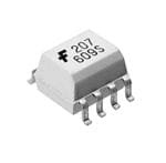
| 描述 | IC OSC SINGLE TIMER 8-SOP计时器和支持产品 SOP-8 Single Timer |
| 产品分类 | |
| 品牌 | Fairchild Semiconductor |
| 产品手册 | |
| 产品图片 |
|
| rohs | 符合RoHS无铅 / 符合限制有害物质指令(RoHS)规范要求 |
| 产品系列 | 时钟和计时器IC,计时器和支持产品,Fairchild Semiconductor LM555CMX- |
| 数据手册 | |
| 产品型号 | LM555CMX |
| 产品种类 | 计时器和支持产品 |
| 供应商器件封装 | 8-SOIC |
| 其它名称 | LM555CMXFSCT |
| 内部定时器数量 | 1 |
| 包装 | 剪切带 (CT) |
| 单位重量 | 143 mg |
| 商标 | Fairchild Semiconductor |
| 安装类型 | 表面贴装 |
| 安装风格 | SMD/SMT |
| 封装 | Reel |
| 封装/外壳 | 8-SOIC(0.154",3.90mm 宽) |
| 封装/箱体 | SOIC-8 Narrow |
| 工作温度 | 0°C ~ 70°C |
| 工厂包装数量 | 3000 |
| 最大功率耗散 | 600 mW |
| 最大工作温度 | + 70 C |
| 最小工作温度 | 0 C |
| 标准包装 | 1 |
| 电压-电源 | 4.5 V ~ 16 V |
| 电流-电源 | 7.5mA |
| 电源电压-最大 | 16 V |
| 电源电压-最小 | 4.5 V |
| 类型 | Standard |
| 系列 | LM555 |
| 计数 | - |
| 频率 | - |


- 商务部:美国ITC正式对集成电路等产品启动337调查
- 曝三星4nm工艺存在良率问题 高通将骁龙8 Gen1或转产台积电
- 太阳诱电将投资9.5亿元在常州建新厂生产MLCC 预计2023年完工
- 英特尔发布欧洲新工厂建设计划 深化IDM 2.0 战略
- 台积电先进制程称霸业界 有大客户加持明年业绩稳了
- 达到5530亿美元!SIA预计今年全球半导体销售额将创下新高
- 英特尔拟将自动驾驶子公司Mobileye上市 估值或超500亿美元
- 三星加码芯片和SET,合并消费电子和移动部门,撤换高东真等 CEO
- 三星电子宣布重大人事变动 还合并消费电子和移动部门
- 海关总署:前11个月进口集成电路产品价值2.52万亿元 增长14.8%


PDF Datasheet 数据手册内容提取
Is Now Part of To learn more about ON Semiconductor, please visit our website at www.onsemi.com Please note: As part of the Fairchild Semiconductor integration, some of the Fairchild orderable part numbers will need to change in order to meet ON Semiconductor’s system requirements. Since the ON Semiconductor product management systems do not have the ability to manage part nomenclature that utilizes an underscore (_), the underscore (_) in the Fairchild part numbers will be changed to a dash (-). This document may contain device numbers with an underscore (_). Please check the ON Semiconductor website to verify the updated device numbers. The most current and up-to-date ordering information can be found at www.onsemi.com. Please email any questions regarding the system integration to Fairchild_questions@onsemi.com. ON Semiconductor and the ON Semiconductor logo are trademarks of Semiconductor Components Industries, LLC dba ON Semiconductor or its subsidiaries in the United States and/or other countries. ON Semiconductor owns the rights to a number of patents, trademarks, copyrights, trade secrets, and other intellectual property. A listing of ON Semiconductor’s product/patent coverage may be accessed at www.onsemi.com/site/pdf/Patent-Marking.pdf. ON Semiconductor reserves the right to make changes without further notice to any products herein. ON Semiconductor makes no warranty, representation or guarantee regarding the suitability of its products for any particular purpose, nor does ON Semiconductor assume any liability arising out of the application or use of any product or circuit, and specifically disclaims any and all liability, including without limitation special, consequential or incidental damages. Buyer is responsible for its products and applications using ON Semiconductor products, including compliance with all laws, regulations and safety requirements or standards, regardless of any support or applications information provided by ON Semiconductor. “Typical” parameters which may be provided in ON Semiconductor data sheets and/or specifications can and do vary in different applications and actual performance may vary over time. All operating parameters, including “Typicals” must be validated for each customer application by customer’s technical experts. ON Semiconductor does not convey any license under its patent rights nor the rights of others. ON Semiconductor products are not designed, intended, or authorized for use as a critical component in life support systems or any FDA Class 3 medical devices or medical devices with a same or similar classification in a foreign jurisdiction or any devices intended for implantation in the human body. Should Buyer purchase or use ON Semiconductor products for any such unintended or unauthorized application, Buyer shall indemnify and hold ON Semiconductor and its officers, employees, subsidiaries, affiliates, and distributors harmless against all claims, costs, damages, and expenses, and reasonable attorney fees arising out of, directly or indirectly, any claim of personal injury or death associated with such unintended or unauthorized use, even if such claim alleges that ON Semiconductor was negligent regarding the design or manufacture of the part. ON Semiconductor is an Equal Opportunity/Affirmative Action Employer. This literature is subject to all applicable copyright laws and is not for resale in any manner.
L M 5 5 January 2013 5 — S i n g LM555 le T i Single Timer m e r Features Description • High-Current Drive Capability: 200 mA The LM555 is a highly stable controller capable of pro- • Adjustable Duty Cycle ducing accurate timing pulses. With a monostable opera- tion, the delay is controlled by one external resistor and • Temperature Stability of 0.005%/°C one capacitor. With astable operation, the frequency and • Timing From μs to Hours duty cycle are accurately controlled by two external • Turn off Time Less Than 2 μs resistors and one capacitor. Applications 8-DIP • Precision Timing • Pulse Generation 1 • Delay Generation 8-SOIC • Sequential Timing 1 Ordering Information Part Number Operating Temperature Range Top Mark Package Packing Method LM555CN LM555CN DIP 8L Rail LM555CM 0 ~ +70°C LM555CM SOIC 8L Rail LM555CMX LM555CM SOIC 8L Tape & Reel © 2002 Fairchild Semiconductor Corporation www.fairchildsemi.com LM555 Rev. 1.1.0 1
L M Block Diagram 5 5 5 — R R R S GGNNDD 1 8 VVcCcC in g l e T i Comp. DiDscishcahrgairnggi nTgra Tnsri.stor m TTrriiggggeerr 2 7 DDiisscchhaarrggee e r OOuuttppuutt 3 OutPut F/F 6 TThhrreesshhoolldd Stage Comp. CTCohonrnettrsroohllold RReesseett 4 5 VVrReEfF VVoollttaaggee Figure 1. Block Diagram Absolute Maximum Ratings Stresses exceeding the absolute maximum ratings may damage the device. The device may not function or be opera- ble above the recommended operating conditions and stressing the parts to these levels is not recommended. In addi- tion, extended exposure to stresses above the recommended operating conditions may affect device reliability. The absolute maximum ratings are stress ratings only. Values are at T = 25°C unless otherwise noted. A Symbol Parameter Value Unit V Supply Voltage 16 V CC T Lead Temperature (Soldering 10s) 300 °C LEAD P Power Dissipation 600 mW D T Operating Temperature Range 0 ~ +70 °C OPR T Storage Temperature Range -65 ~ +150 °C STG © 2002 Fairchild Semiconductor Corporation www.fairchildsemi.com LM555 Rev. 1.1.0 2
L M Electrical Characteristics 5 5 5 Values are at T = 25°C, V = 5 ~ 15 V unless otherwise specified. A CC — Parameter Symbol Conditions Min. Typ. Max. Unit S Supply Voltage VCC 4.5 16.0 V in g Supply Current (Low Stable) (1) I VCC = 5 V, RL = ∞ 3 6 mA le CC V = 15 V, R = ∞ 7.5 15.0 mA T CC L i m Timing Error (Monostable) Initial Accuracy (2) ACCUR R = 1 kΩ to100 kΩ 1.0 3.0 % er A Drift with Temperature (3) Δt / ΔT C = 0.1 μF 50 ppm / °C Drift with Supply Voltage (3) Δt / ΔV 0.1 0.5 % / V CC Timing Error (Astable) ACCUR 2.25 % InItial Accuracy (2) R = 1 kΩ to 100kΩ A Drift with Temperature (3) Δt / ΔT C = 0.1 μF 150 ppm / °C Drift with Supply Voltage (3) Δt / ΔV 0.3 % / V CC V = 15 V 9.0 10.0 11.0 V CC Control Voltage V C V = 5 V 2.60 3.33 4.00 V CC V = 15 V 10.0 V CC Threshold Voltage V TH V = 5V 3.33 V CC Threshold Current (4) I 0.10 0.25 μA TH V = 5 V 1.10 1.67 2.20 V CC Trigger Voltage V TR V = 15 V 4.5 5.0 5.6 V CC Trigger Current I V = 0 V 0.01 2.00 μA TR TR Reset Voltage V 0.4 0.7 1.0 V RST Reset Current I 0.1 0.4 mA RST I = 10 mA 0.06 0.25 V SINK V = 15 V CC Low Output Voltage V I = 50 mA 0.30 0.75 V OL SINK V = 5 V, I = 5 mA 0.05 0.35 V CC SINK I = 200 mA 12.5 V SOURCE V = 15 V CC High Output Voltage V I = 100 mA 12.75 13.30 V OH SOURCE V = 5 V, I = 100 mA 2.75 3.30 V CC SOURCE Rise Time of Output(3) t 100 ns R Fall Time of Output(3) t 100 ns F Discharge Leakage Current I 20 100 nA LKG Notes: 1. When the output is high, the supply current is typically 1 mA less than at V = 5 V. CC 2. Tested at V = 5.0 V and V = 15 V. CC CC 3. These parameters, although guaranteed, are not 100% tested in production. 4. This determines the maximum value of RA + RB for 15 V operation, the maximum total R = 20 MΩ, and for 5 V operation, the maximum total R = 6.7 MΩ. © 2002 Fairchild Semiconductor Corporation www.fairchildsemi.com LM555 Rev. 1.1.0 3
L M Application Information 5 5 5 Table 1 below is the basic operating table of 555 timer. — Table 1. Basic Operating Table S i n Discharging g Reset V V Output l TR TH Transistor e (PIN 4) (PIN 2) (PIN 6) (PIN 3) T (PIN 7) i m Low X X Low ON e r High < 1/3 V X High OFF CC High > 1/3 V > 2/3 V Low ON CC CC High > 1/3 V < 2/3 V Previous State CC CC When the low signal input is applied to the reset terminal, the timer output remains low regardless of the threshold volt- age or the trigger voltage. Only when the high signal is applied to the reset terminal, the timer's output changes accord- ing to threshold voltage and trigger voltage. When the threshold voltage exceeds 2/3 of the supply voltage while the timer output is high, the timer's internal dis- charge transistor turns on, lowering the threshold voltage to below 1/3 of the supply voltage. During this time, the timer output is maintained low. Later, if a low signal is applied to the trigger voltage so that it becomes 1/3 of the supply volt- age, the timer's internal discharge transistor turns off, increasing the threshold voltage and driving the timer output again at high. 1. Monostable Operation +Vcc 102 RE4SET V8cc RA 101 R=A1kΩ 10kΩ 100kΩ 1MΩ 10MΩ Trigger DISCH 7 uF) 100 2 TRIG nce( THRES 6 acita 10-1 p a C 3 OUT C1 10-2 CONT 5 GND RL 1 C2 10-3 10-5 10-4 10-3 10-2 10-1 100 101 102 Time Delay(s) Figure2. Monostable Circuit Figure 3. Resistance and Capacitance vs. Time Delay (t ) D Figure 4. Waveforms of Monostable Operation © 2002 Fairchild Semiconductor Corporation www.fairchildsemi.com LM555 Rev. 1.1.0 4
L M 1. Monostable Operation 5 5 Figure 2 illustrates a monostable circuit. In this mode, the timer generates a fixed pulse whenever the trigger voltage 5 falls below VCC/3. When the trigger pulse voltage applied to the #2 pin falls below VCC/3 while the timer output is low, — the timer's internal flip-flop turns the discharging transistor off and causes the timer output to become high by charging S the external capacitor C1 and setting the flip-flop output at the same time. i n The voltage across the external capacitor C1, VC1 increases exponentially with the time constant t = RA*C and g reaches 2 VCC/3 at tD = 1.1 RA*C. Hence, capacitor C1 is charged through resistor RA. The greater the time constant le R C, the longer it takes for the V to reach 2 V /3. In other words, the time constant R C controls the output pulse T A C1 CC A i width. m When the applied voltage to the capacitor C1 reaches 2 V /3, the comparator on the trigger terminal resets the flip- e CC r flop, turning the discharging transistor on. At this time, C1 begins to discharge and the timer output converts to low. In this way, the timer operating in the monostable repeats the above process. Figure 3 shows the time constant rela- tionship based on R and C. Figure 4 shows the general waveforms during the monostable operation. A It must be noted that, for a normal operation, the trigger pulse voltage needs to maintain a minimum of V /3 before CC the timer output turns low. That is, although the output remains unaffected even if a different trigger pulse is applied while the output is high, it may be affected and the waveform does not operate properly if the trigger pulse voltage at the end of the output pulse remains at below V /3. Figure 5 shows such a timer output abnormality. CC Figure 5. Waveforms of Monostable Operation (abnormal) 2. Astable Operation +Vcc 100 RA (RA+2RB) 4 8 10 RESET Vcc 1kΩ 2 TRIG DISCH 7 RB nce(uF) 1 100kΩ10kΩ THRES 6 acita 0.1 1MΩ Cap 10MΩ 3 OUT C1 CONT 5 0.01 GND RL 1 C2 1E-3 100m 1 10 100 1k 10k 100k Frequency(Hz) Figure 6. A Stable Circuit Figure 7. Capacitance and Resistance vs. Frequency © 2002 Fairchild Semiconductor Corporation www.fairchildsemi.com LM555 Rev. 1.1.0 5
L M 5 5 5 — S i n g l e T i m e r Figure 8. Waveforms of Astable Operation An astable timer operation is achieved by adding resistor R to Figure 2 and configuring as shown on Figure 6. In the B astable operation, the trigger terminal and the threshold terminal are connected so that a self-trigger is formed, operat- ing as a multi-vibrator. When the timer output is high, its internal discharging transistor. turns off and the V increases C1 by exponential function with the time constant (R +R )*C. A B When the V , or the threshold voltage, reaches 2 V /3; the comparator output on the trigger terminal becomes C1 CC high, resetting the F/F and causing the timer output to become low. This turns on the discharging transistor and the C1 discharges through the discharging channel formed by R and the discharging transistor. When the V falls below B C1 V /3, the comparator output on the trigger terminal becomes high and the timer output becomes high again. The dis- CC charging transistor turns off and the V rises again. C1 In the above process, the section where the timer output is high is the time it takes for the V to rise from V /3 to 2 C1 CC V /3, and the section where the timer output is low is the time it takes for the VC1 to drop from 2 V /3 to V /3. CC CC CC When timer output is high, the equivalent circuit for charging capacitor C1 is as follows: R R A B Vcc C1 Vc1(0-)=Vcc/3 dv V –V(0-) C --------c---1--=-----c---c----------------------- (1) 1 dt R +R A B V (0+) = V ⁄3 (2) C1 CC -–------------------t------------------- (R +R )C1 V (t) = V 1–2---e A B (3) C1 CC 3 Since the duration of the timer output high state (t ) is the amount of time it takes for the V (t) to reach 2 V /3, L C1 CC tH V (t) = 2---V =V 1–2---e-–(---R-----A-----+-----R-----B----)--C-----1--- (4) C1 3 CC CC 3 t = C (R +R )In2=0.693(R +R )C (5) H 1 A B A B 1 © 2002 Fairchild Semiconductor Corporation www.fairchildsemi.com LM555 Rev. 1.1.0 6
L M The equivalent circuit for discharging capacitor C1, when timer output is low is, as follows: 5 5 5 — R B S i n g l C1 V (0-)=2Vcc/3 R e C1 D T i m e r dv C --------C----1---+-----------1------------V =0 (6) 1 dt R +R C1 A B t -------------------------------------- (R +R )C1 V (t)=2---V A D (7) C1 3 e CC Since the duration of the timer output low state (t ) is the amount of time it takes for the VC1(t) to reach V /3, L CC t -------------------L------------------- 1---V = 2---V (RA+RD)C1 (8) 3 CC 3 e CC t = C (R +R )In2=0.693(R +R )C (9) L 1 B D B D 1 Since R is normally R >>R although related to the size of discharging transistor, D B D t = 0.693R C (10) L B 1 Consquently, if the timer operates in astable, the period is the same with 't = t +t = 0.693(RA+R )C +0.693R C = 0.693(R +2R )C ' H L B 1 B 1 A B 1 because the period is the sum of the charge time and discharge time. Since frequency is the reciprocal of the period, the following applies: frequency, f = 1--- = ---------------1---.--4---4----------------- (11) t (R +2R )C A B 1 © 2002 Fairchild Semiconductor Corporation www.fairchildsemi.com LM555 Rev. 1.1.0 7
L M 3. Frequency Divider 5 5 5 By adjusting the length of the timing cycle, the basic circuit of Figure 1 can be made to operate as a frequency divider. — Figure 9. illustrates a divide-by-three circuit that makes use of the fact that retriggering cannot occur during the timing cycle. S i n g l e T i m e r Figure 9. Waveforms of Frequency Divider Operation 4. Pulse Width Modulation The timer output waveform may be changed by modulating the control voltage applied to the timer's pin 5 and chang- ing the reference of the timer's internal comparators. Figure 10 illustrates the pulse width modulation circuit. When the continuous trigger pulse train is applied in the monostable mode, the timer output width is modulated accord- ing to the signal applied to the control terminal. Sine wave, as well as other waveforms, may be applied as a signal to the control terminal. Figure 11 shows the example of pulse width modulation waveform. +Vcc R A 4 8 RESET Vcc 7 Trigger DISCH 2 TRIG 6 THRES Output 3 OUT Input GND CONT 5 C 1 Figure 10. Circuit for Pulse Width Modulation Figure 11. Waveforms of Pulse Width Modulation © 2002 Fairchild Semiconductor Corporation www.fairchildsemi.com LM555 Rev. 1.1.0 8
L M 5. Pulse Position Modulation 5 5 5 If the modulating signal is applied to the control terminal while the timer is connected for the astable operation, as in — Figure 12, the timer becomes a pulse position modulator. In the pulse position modulator, the reference of the timer's internal comparators is modulated, which modulates the S i timer output according to the modulation signal applied to the control terminal. n g Figure 13 illustrates a sine wave for modulation signal and the resulting output pulse position modulation; however, any l e wave shape be used. T i m e r +Vcc R A 4 8 RESET Vcc 7 DISCH 2 TRIG R B 6 THRES Output 3 OUT Modulation CONT 5 C GND 1 Figure 12. Circuit for Pulse Position Modluation Figure 13. Wafeforms of pulse position modulation 6. Linear Ramp When the pull-up resistor RA in the monostable circuit shown in Figure 2 is replaced with constant current source, the V increases linearly, generating a linear ramp. Figure 14 shows the linear ramp generating circuit and Figure 15 illus- C1 trates the generated linear ramp waveforms. +Vcc R R1 E 4 8 RESET Vcc 7 DISCH Q1 2 TRIG THRES 6 R2 Output 3 OUT C1 CONT 5 GND 1 C2 Figure 14. Circuit for Linear Ramp Figure 15. Waveforms of Linear Ramp © 2002 Fairchild Semiconductor Corporation www.fairchildsemi.com LM555 Rev. 1.1.0 9
L M In Figure 14, current source is created by PNP transistor Q1 and resistor R1, R2, and RE. 5 5 5 V –V — I = -----C----C---------------E--- (12) C R S E i n Here, V g E is l e R T V = V +------------2----------V (13) im E BE R +R CC 1 2 e For example, if V = 15 V, R = 20 kΩ, R1 = 5 kΩ, R2 = 10 kΩ, and V = 0.7 V, r CC E BE V =0.7 V+10 V=10.7 V, and E I =(15-10.7) / 20 k=0.215 mA. C When the trigger starts in a timer configured as shown in Figure 14, the current flowing through capacitor C1 becomes a constant current generated by PNP transistor and resistors. Hence, the V is a linear ramp function as shown in Figure 15. The gradient S of the linear ramp function is defined as C follows: V S = -----p-----–----p-- (14) t Here the Vp-p is the peak-to-peak voltage. If the electric charge amount accumulated in the capacitor is divided by the capacitance, the V comes out as follows: C V = Q/C (15) The above equation divided on both sides by t gives: V---- = Q-------§-----t- (16) t C and may be simplified into the following equation: S = I/C (17) In other words, the gradient of the linear ramp function appearing across the capacitor can be obtained by using the constant current flowing through the capacitor. If the constant current flow through the capacitor is 0.215 mA and the capacitance is 0.02 μF, the gradient of the ramp function at both ends of the capacitor is S = 0.215 m / 0.022 μ = 9.77 V/ms. © 2002 Fairchild Semiconductor Corporation www.fairchildsemi.com LM555 Rev. 1.1.0 10
L M Physical Dimensions 5 5 5 8-DIP — S i n g l A ..430703 [190.4.165] e T .036 [0.9 TYP] im e (.092) [Ø2.337] r PIN #1 (.032) [R0.813] .250±.005 [6.35±0.13] PIN #1 B TOP VIEW TOP VIEW OPTION 1 OPTION 2 ..007405 [11..7184] .310±.010 [7.87±0.25] .130±.005 [3.3±0.13] 7° TYP .210 MAX [5.33] 7° TYP C .015 MIN ..002115 [00..5337] ..114205[ 0[.333..851]57] [.73.0602] .001[.025] C .100 .430 MAX [2.54] [10.92] NOTES: .060 MAX [1.52] A . VCAORNIFAOTIROMNSS TBOA JEDEC REGISTRATION MS-001, .010+-..000005 [0.254+-00..010207] B. CONTROLING DIMENSIONS ARE IN INCHES REFERENCE DIMENSIONS ARE IN MILLIMETERS C. DOES NOT INCLUDE MOLD FLASH OR PROTRUSIONS. MOLD FLASH OR PROTRUSIONS SHALL NOT EXCEED .010 INCHES OR 0.25MM. D. DOES NOT INCLUDE DAMBAR PROTRUSIONS. DAMBAR PROTRUSIONS SHALL NOT EXCEED .010 INCHES OR 0.25MM. E. DIMENSIONING AND TOLERANCING PER ASME Y14.5M-1994. N08EREVG Figure 16. 8-Lead, DIP, JEDEC MS-001, 300" WIDE Package drawings are provided as a service to customers considering Fairchild components. Drawings may change in any manner without notice. Please note the revision and/or date on the drawing and contact a Fairchild Semiconductor representative to verify or obtain the most recent revision. Package specifications do not expand the terms of Fairchild’s worldwide terms and conditions, specifically the warranty therein, which covers Fairchild products. Always visit Fairchild Semiconductor’s online packaging area for the most recent package drawings: http://www.fairchildsemi.com/packaging/. For current tape and reel specifications, visit Fairchild Semiconductor’s online packaging area: http://www.fairchildsemi.com/products/discrete/pdf/8dip_tr.pdf. © 2002 Fairchild Semiconductor Corporation www.fairchildsemi.com LM555 Rev. 1.1.0 11
L M Physical Dimensions (continued) 5 5 5 8-SOIC — S i n g l e T i m e r Figure 17. 8-Lead, SOIC,JEDEC MS-012, 150" NARROW BODY Package drawings are provided as a service to customers considering Fairchild components. Drawings may change in any manner without notice. Please note the revision and/or date on the drawing and contact a Fairchild Semiconductor representative to verify or obtain the most recent revision. Package specifications do not expand the terms of Fairchild’s worldwide terms and conditions, specifically the warranty therein, which covers Fairchild products. Always visit Fairchild Semiconductor’s online packaging area for the most recent package drawings: http://www.fairchildsemi.com/packaging/. For current tape and reel specifications, visit Fairchild Semiconductor’s online packaging area: http://www.fairchildsemi.com/dwg/M0/M08A.pdf. © 2002 Fairchild Semiconductor Corporation www.fairchildsemi.com LM555 Rev. 1.1.0 12
TRADEMARKS The following includes registered and unregistered trademarks and service marks, owned by Fairchild Semiconductor and/or its global subsidiaries, and is not intended to be an exhaustive list of all such trademarks. 2Cool(cid:165) F-PFS(cid:165) PowerTrench® The Power Franchise® AccuPower(cid:165) FRFET® PowerXS™ AX-CAP(cid:165)* Global Power ResourceSM Programmable Active Droop(cid:165) BitSiC(cid:165) GreenBridge(cid:165) QFET® TinyBoost(cid:165) Build it Now(cid:165) Green FPS(cid:165) QS(cid:165) TinyBuck(cid:165) CCoorreePPOLUWSE(cid:165)R(cid:165) GGrmeaexn(cid:165) FPS(cid:165) e-Series(cid:165) QRaupieidt CSoenrifeigs(cid:165)ure(cid:165) TTiinnyyLCoaglcic(cid:165)® CROSSVOLT(cid:165) GTO(cid:165) (cid:165) TINYOPTO(cid:165) CTL(cid:165) IntelliMAX(cid:165) Saving our world, 1mW/W/kW at a time™ TinyPower(cid:165) Current Transfer Logic(cid:165) ISOPLANAR(cid:165) SignalWise(cid:165) TinyPWM(cid:165) DEUXPEED® Making Small Speakers Sound Louder SmartMax(cid:165) TinyWire(cid:165) Dual Cool™ and Better™ EcoSPARK® MegaBuck(cid:165) SMART START(cid:165) TranSiC(cid:165) Solutions for Your Success(cid:165) TriFault Detect(cid:165) EfficientMax(cid:165) MICROCOUPLER(cid:165) SPM® TRUECURRENT®* ESBC(cid:165) MicroFET(cid:165) STEALTH(cid:165) (cid:80)SerDes(cid:165) ® MicroPak(cid:165) SuperFET® FFaaiirrcchhiilldd ®Semiconductor® MMiilclerorDPraikve2(cid:165)(cid:165) SSuuppeerrSSOOTT(cid:165)(cid:165)-3-6 UHC® FFAACCTT® Quiet Series(cid:165) MmWotiSonaMvear(cid:165)x(cid:165) SSuuppreerMSOOTS(cid:165)®-8 UUlntriFaE FTR(cid:165)FET(cid:165) FFAasStTvC®ore(cid:165) OOOPpPtTToOOHPLiTOL(cid:165)AGNICA®R® SSyynncc-FLEoTc(cid:165)k™ VVCisXua(cid:165)lMax(cid:165) FETBench(cid:165) ®* VoltagePlus(cid:165) FPS(cid:165) XS™ ® * Trademarks of System General Corporation, used under license by Fairchild Semiconductor. DISCLAIMER FAIRCHILD SEMICONDUCTOR RESERVES THE RIGHT TO MAKE CHANGES WITHOUT FURTHER NOTICE TO ANY PRODUCTS HEREIN TO IMPROVE RELIABILITY, FUNCTION, OR DESIGN. FAIRCHILD DOES NOT ASSUME ANY LIABILITY ARISING OUT OF THE APPLICATION OR USE OF ANY PRODUCT OR CIRCUIT DESCRIBED HEREIN; NEITHER DOES IT CONVEY ANY LICENSE UNDER ITS PATENT RIGHTS, NOR THE RIGHTS OF OTHERS. THESE SPECIFICATIONS DO NOT EXPAND THE TERMS OF FAIRCHILD’S WORLDWIDE TERMS AND CONDITIONS, SPECIFICALLY THE WARRANTY THEREIN, WHICH COVERS THESE PRODUCTS. LIFE SUPPORT POLICY FAIRCHILD’S PRODUCTS ARE NOT AUTHORIZED FOR USE AS CRITICAL COMPONENTS IN LIFE SUPPORT DEVICES OR SYSTEMS WITHOUT THE EXPRESS WRITTEN APPROVAL OF FAIRCHILD SEMICONDUCTOR CORPORATION. As used herein: 1. Life support devices or systems are devices or systems which, (a) are 2. A critical component in any component of a life support, device, or intended for surgical implant into the body or (b) support or sustain system whose failure to perform can be reasonably expected to life, and (c) whose failure to perform when properly used in cause the failure of the life support device or system, or to affect its accordance with instructions for use provided in the labeling, can be safety or effectiveness. reasonably expected to result in a significant injury of the user. ANTI-COUNTERFEITING POLICY Fairchild Semiconductor Corporation's Anti-Counterfeiting Policy. Fairchild's Anti-Counterfeiting Policy is also stated on our external website, www.fairchildsemi.com, under Sales Support. Counterfeiting of semiconductor parts is a growing problem in the industry. All manufacturers of semiconductor products are experiencing counterfeiting of their parts. Customers who inadvertently purchase counterfeit parts experience many problems such as loss of brand reputation, substandard performance, failed applications, and increased cost of production and manufacturing delays. Fairchild is taking strong measures to protect ourselves and our customers from the proliferation of counterfeit parts. Fairchild strongly encourages customers to purchase Fairchild parts either directly from Fairchild or from Authorized Fairchild Distributors who are listed by country on our web page cited above. Products customers buy either from Fairchild directly or from Authorized Fairchild Distributors are genuine parts, have full traceability, meet Fairchild's quality standards for handling and storage and provide access to Fairchild's full range of up-to-date technical and product information. Fairchild and our Authorized Distributors will stand behind all warranties and will appropriately address any warranty issues that may arise. Fairchild will not provide any warranty coverage or other assistance for parts bought from Unauthorized Sources. Fairchild is committed to combat this global problem and encourage our customers to do their part in stopping this practice by buying direct or from authorized distributors. PRODUCT STATUS DEFINITIONS Definition of Terms Datasheet Identification Product Status Definition Datasheet contains the design specifications for product development. Specifications may change Advance Information Formative / In Design in any manner without notice. Datasheet contains preliminary data; supplementary data will be published at a later date. Fairchild Preliminary First Production Semiconductor reserves the right to make changes at any time without notice to improve design. Datasheet contains final specifications. Fairchild Semiconductor reserves the right to make No Identification Needed Full Production changes at any time without notice to improve the design. Datasheet contains specifications on a product that is discontinued by Fairchild Semiconductor. Obsolete Not In Production The datasheet is for reference information only. Rev. I63 © Fairchild Semiconductor Corporation www.fairchildsemi.com
ON Semiconductor and are trademarks of Semiconductor Components Industries, LLC dba ON Semiconductor or its subsidiaries in the United States and/or other countries. ON Semiconductor owns the rights to a number of patents, trademarks, copyrights, trade secrets, and other intellectual property. A listing of ON Semiconductor’s product/patent coverage may be accessed at www.onsemi.com/site/pdf/Patent−Marking.pdf. ON Semiconductor reserves the right to make changes without further notice to any products herein. ON Semiconductor makes no warranty, representation or guarantee regarding the suitability of its products for any particular purpose, nor does ON Semiconductor assume any liability arising out of the application or use of any product or circuit, and specifically disclaims any and all liability, including without limitation special, consequential or incidental damages. Buyer is responsible for its products and applications using ON Semiconductor products, including compliance with all laws, regulations and safety requirements or standards, regardless of any support or applications information provided by ON Semiconductor. “Typical” parameters which may be provided in ON Semiconductor data sheets and/or specifications can and do vary in different applications and actual performance may vary over time. All operating parameters, including “Typicals” must be validated for each customer application by customer’s technical experts. ON Semiconductor does not convey any license under its patent rights nor the rights of others. ON Semiconductor products are not designed, intended, or authorized for use as a critical component in life support systems or any FDA Class 3 medical devices or medical devices with a same or similar classification in a foreign jurisdiction or any devices intended for implantation in the human body. Should Buyer purchase or use ON Semiconductor products for any such unintended or unauthorized application, Buyer shall indemnify and hold ON Semiconductor and its officers, employees, subsidiaries, affiliates, and distributors harmless against all claims, costs, damages, and expenses, and reasonable attorney fees arising out of, directly or indirectly, any claim of personal injury or death associated with such unintended or unauthorized use, even if such claim alleges that ON Semiconductor was negligent regarding the design or manufacture of the part. ON Semiconductor is an Equal Opportunity/Affirmative Action Employer. This literature is subject to all applicable copyright laws and is not for resale in any manner. PUBLICATION ORDERING INFORMATION LITERATURE FULFILLMENT: N. American Technical Support: 800−282−9855 Toll Free ON Semiconductor Website: www.onsemi.com Literature Distribution Center for ON Semiconductor USA/Canada 19521 E. 32nd Pkwy, Aurora, Colorado 80011 USA Europe, Middle East and Africa Technical Support: Order Literature: http://www.onsemi.com/orderlit Phone: 303−675−2175 or 800−344−3860 Toll Free USA/Canada Phone: 421 33 790 2910 Fax: 303−675−2176 or 800−344−3867 Toll Free USA/Canada Japan Customer Focus Center For additional information, please contact your local Email: orderlit@onsemi.com Phone: 81−3−5817−1050 Sales Representative © Semiconductor Components Industries, LLC www.onsemi.com www.onsemi.com 1
Mouser Electronics Authorized Distributor Click to View Pricing, Inventory, Delivery & Lifecycle Information: O N Semiconductor: LM555CMX LM555CN LM555CM