ICGOO在线商城 > 集成电路(IC) > PMIC - 稳压器 - DC DC 切换控制器 > LM5027AMH/NOPB

 Datasheet下载
- 型号: LM5027AMH/NOPB
- 制造商: Texas Instruments
- 库位|库存: xxxx|xxxx
- 要求:
| 数量阶梯 | 香港交货 | 国内含税 |
| +xxxx | $xxxx | ¥xxxx |
查看当月历史价格
查看今年历史价格
LM5027AMH/NOPB产品简介:
ICGOO电子元器件商城为您提供LM5027AMH/NOPB由Texas Instruments设计生产,在icgoo商城现货销售,并且可以通过原厂、代理商等渠道进行代购。 LM5027AMH/NOPB价格参考¥11.19-¥11.77。Texas InstrumentsLM5027AMH/NOPB封装/规格:PMIC - 稳压器 - DC DC 切换控制器, 正激转换器 稳压器 正,可提供隔离 输出 升压/降压 DC-DC 控制器 IC 20-HTSSOP。您可以下载LM5027AMH/NOPB参考资料、Datasheet数据手册功能说明书,资料中有LM5027AMH/NOPB 详细功能的应用电路图电压和使用方法及教程。
Texas Instruments的LM5027AMH/NOPB是一款高效的同步降压DC-DC切换控制器,广泛应用于需要高效电源管理的场景。以下是其主要应用场景:

1. 工业自动化:在工业控制系统中,如PLC(可编程逻辑控制器)、传感器和执行器等设备,LM5027AMH/NOPB可以提供稳定的电源供应,确保系统在高噪声环境下稳定运行。

2. 通信基础设施:适用于基站、路由器、交换机等通信设备。这些设备通常要求高效率和低功耗的电源解决方案,以减少散热并提高可靠性。

3. 汽车电子:用于车载信息娱乐系统、ADAS(高级驾驶辅助系统)等。该芯片能够承受汽车环境中的电压波动和温度变化,确保系统的可靠性和安全性。

4. 消费类电子产品:如笔记本电脑、平板电脑和智能手表等便携式设备。通过高效的电源管理,延长电池续航时间,并减小设备体积。

5. 医疗设备:在便携式医疗设备(如血糖仪、心率监测仪)和固定式医疗设备(如超声波设备、X光机)中,提供稳定的电源支持,确保设备的准确性和安全性。

6. 数据中心和服务器:为服务器和存储设备提供高效电源管理,降低能耗,提升整体性能。

7. 太阳能逆变器和其他可再生能源系统:在这些系统中,LM5027AMH/NOPB可以有效地将不稳定的输入电压转换为稳定的输出电压,确保系统的稳定运行。

8. 物联网(IoT)设备:如智能家居设备、传感器节点等,这些设备通常需要长时间工作且功耗较低,LM5027AMH/NOPB可以提供高效的电源管理,延长设备的使用寿命。

总之,LM5027AMH/NOPB凭借其高效、灵活和可靠的特性,适用于各种需要高性能电源管理的场景,特别是在对效率和稳定性有较高要求的应用中表现出色。
| 参数 | 数值 |
| 产品目录 | 集成电路 (IC)半导体 |
| Cuk | 无 |
| 描述 | IC REG CTRLR PWM VM 20TSSOP开关控制器 Active Clamp Pwm W/3A Sr Drv |
| 产品分类 | |
| 品牌 | Texas Instruments |
| 产品手册 | |
| 产品图片 |
|
| rohs | 符合RoHS无铅 / 符合限制有害物质指令(RoHS)规范要求 |
| 产品系列 | 电源管理 IC,开关控制器 ,Texas Instruments LM5027AMH/NOPB- |
| 数据手册 | |
| 产品型号 | LM5027AMH/NOPB |
| PCN设计/规格 | |
| PWM类型 | 电压模式 |
| 上升时间 | 15 ns |
| 下降时间 | 13 ns |
| 产品种类 | 开关控制器 |
| 倍增器 | 无 |
| 其它名称 | LM5027AMH |
| 分频器 | 无 |
| 包装 | 管件 |
| 升压 | 是 |
| 占空比 | 75% |
| 占空比-最大 | 90 % |
| 反向 | 是 |
| 反激式 | 无 |
| 同步管脚 | No |
| 商标 | Texas Instruments |
| 安装风格 | SMD/SMT |
| 封装/外壳 | 20-TSSOP(0.173",4.40mm 宽)裸焊盘 |
| 封装/箱体 | eTSSOP-20 |
| 工作温度 | -40°C ~ 125°C |
| 工作电源电压 | 8 V to 105 V |
| 工作电源电流 | 6 mA |
| 工厂包装数量 | 73 |
| 开关频率 | 1 MHz |
| 拓扑结构 | Forward Active Clamp |
| 最大工作温度 | + 125 C |
| 最小工作温度 | - 40 C |
| 标准包装 | 73 |
| 电压-电源 | 8 V ~ 15 V |
| 类型 | Voltage Mode PWM Controllers |
| 系列 | LM5027A |
| 输出数 | 1 |
| 输出电流 | 65 mA |
| 输出端数量 | 3 Output |
| 配用 | /product-detail/zh/LM5027A-EVAL%2FNOPB/LM5027A-EVAL%2FNOPB-ND/3640505 |
| 降压 | 是 |
| 隔离式 | 是 |
| 频率-最大值 | 1MHz |


- 商务部:美国ITC正式对集成电路等产品启动337调查
- 曝三星4nm工艺存在良率问题 高通将骁龙8 Gen1或转产台积电
- 太阳诱电将投资9.5亿元在常州建新厂生产MLCC 预计2023年完工
- 英特尔发布欧洲新工厂建设计划 深化IDM 2.0 战略
- 台积电先进制程称霸业界 有大客户加持明年业绩稳了
- 达到5530亿美元!SIA预计今年全球半导体销售额将创下新高
- 英特尔拟将自动驾驶子公司Mobileye上市 估值或超500亿美元
- 三星加码芯片和SET,合并消费电子和移动部门,撤换高东真等 CEO
- 三星电子宣布重大人事变动 还合并消费电子和移动部门
- 海关总署:前11个月进口集成电路产品价值2.52万亿元 增长14.8%


PDF Datasheet 数据手册内容提取
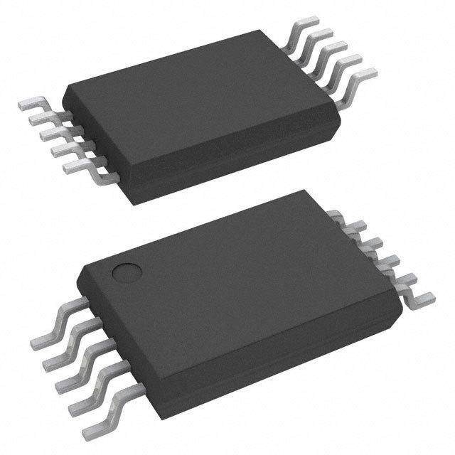
LM5027A www.ti.com SNVS642B–APRIL2010–REVISEDMARCH2013 Voltage Mode Active Clamp Controller CheckforSamples:LM5027A FEATURES DESCRIPTION 1 • Voltage-ModeControl The LM5027A is a functional variant of the LM5027 2 active clamp PWM controller. The functional • LineFeed-ForwardPWMRamp difference of the LM5027A is that the maximum duty • Internal105VRatedStart-UpBiasRegulator cycleoftheLM5027Aisdecreasedfrom91%to71%. • ProgrammableLineUnder-VoltageLockout In addition, the oscillator timing equation has been (UVLO)withAdjustableHysteresis modified. • VersatileDualModeOver-CurrentProtection The LM5027A pulse-width modulation (PWM) controller contains all of the features necessary to • ProgrammableVolt-SecondLimiterandSoft- implement power converters utilizing the Active Start Clamp / Reset technique. With the active clamp • ProgrammableSynchronousRectifierSoft- technique, higher efficiencies and greater power StartandStop densities can be realized compared to conventional • Precise500mVOver-CurrentComparator catch winding or RDC clamp / reset techniques. Three control outputs are provided: the main power • CurrentSenseLeadingEdgeBlanking switch control (OUTA), the active clamp switch • ProgrammableOscillatorWith1MHz control (OUTB), and secondary side synchronous MaximumFrequencyandSynchronization rectifier control (OUTSR). The timing between the Capability control outputs is adjustable with external resistors • Precision5VReference that program internal precision timers. This controller is designed for high-speed operation including an • ProgrammableTimeDelaysBetweenOutputs oscillator frequency range up to 1 MHz and total • A70%MaximumDutyCycle PWM propagation delays less than 50 ns. The LM5027A includes a high-voltage startup regulator with a maximum input voltage rating of 105V. Additional features include Line Under Voltage Lockout (UVLO), separate soft-start of main and synchronousrectifieroutputs,atimerforhiccupmode current limiting, a precision reference, and thermal shutdown. Packages • HTSSOP-20 • WQFN-24 1 Pleasebeawarethatanimportantnoticeconcerningavailability,standardwarranty,anduseincriticalapplicationsof TexasInstrumentssemiconductorproductsanddisclaimerstheretoappearsattheendofthisdatasheet. Alltrademarksarethepropertyoftheirrespectiveowners. 2 PRODUCTIONDATAinformationiscurrentasofpublicationdate. Copyright©2010–2013,TexasInstrumentsIncorporated Products conform to specifications per the terms of the Texas Instruments standard warranty. Production processing does not necessarilyincludetestingofallparameters.
LM5027A SNVS642B–APRIL2010–REVISEDMARCH2013 www.ti.com Typical Application Circuit VIN VOUT LM5027A CS VCC Vin OUTA RAMP OUTB UVLO OUTSR TIME3 COMP REF SSSR ERROR AMP and OTP TIME2 ISOLATION RT RES TIME1 SS AGND PGND Figure1. SimplifiedActiveClampConverter 2 SubmitDocumentationFeedback Copyright©2010–2013,TexasInstrumentsIncorporated ProductFolderLinks:LM5027A
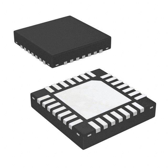
LM5027A www.ti.com SNVS642B–APRIL2010–REVISEDMARCH2013 Connection Diagram VIN 1 20 UVLO O RAMP 2 19 OTP NC VIN NC UVL OTP TIME3 3 18 SSSR 24 23 22 21 20 TIME2 4 17 RES TIME1 5 16 SS RAMP 1 19 SSSR EP AGND 6 15 CS TIME 3 2 18 RES RT 7 14 VCC COMP 8 13 PGND TIME 2 3 17 SS REF 9 12 OUTSR TIME 1 4 16 CS OUTB 10 11 OUTA EP AGND 5 15 VCC RT 6 14 VCC COMP 7 13 PGND 8 9 10 11 12 F B A R D E T T S N R U U T G O O OU P Figure2.20-LeadHTSSOP Figure3.24-LeadWQFN Table1.PinDescriptions Pin(1) Name Description ApplicationInformation 1 VIN Inputvoltagesource InputtotheStart-upRegulator.Operatinginputrangeis13Vto90V.TheAbsolute MaximumRatingis105V.Forpowersourcesoutsideofthisrange,theLM5027A canbebiaseddirectlyatVCCbyanexternalregulator. 2 RAMP Feed-forwardmodulation AnexternalRCcircuitfromVINsetsthePWMrampslope.Thispinisdischarged ramp attheconclusionofeverycyclebyaninternalFET.Aninternalcomparator terminatesthePWMpulseiftheRAMPpinexceeds2.5Vthuslimitingthe maximumvolt-secondproducttothetransformerprimary. 3 TIME3 Overlapdelay3 Anexternalresistorsetstheoverlapdelayfortheactiveclampoutput.TheR TIME3 resistorconnectedbetweenTIME3andAGNDsetstheOUTAturn-off(falling edge)toOUTBturn-on(fallingedge)pulsedelay.SeeFigure26. 4 TIME2 Overlapdelay2 AnexternalresistorsetstheoverlapdelayfortheOUTSRoutput.TheR TIME2 resistorconnectedbetweenTIME2andAGNDsetstheOUTAturn-off(falling edge)toOUTSRturn-on(risingedge)pulsedelay.SeeFigure26. 5 TIME1 Overlapdelay1 Anexternalresistorsetstheoverlapdelayfortheactiveclampoutput.TheR TIME1 resistorconnectedbetweenTIME1andAGNDsetstheOUTBandOUTSRturn- offtoOUTAturn-onpulsedelay.SeeFigure26. 6 AGND Analogground ConnectdirectlytoPowerGround. 7 RT Oscillatorfrequencycontrol Normallybiasedat2Vbyaninternalamplifier.Anexternalresistorconnected andsyncclockinput betweenRTandAGNDsetstheinternaloscillatorfrequency.Theinternal oscillatorcanbesynchronizedtoanexternalclockwithafrequencyhigherthan thefreerunningfrequencysetbytheRTresistor. 8 COMP Inputtothepulsewidth Anexternalopto-couplerconnectedtotheCOMPpinsourcescurrentintoan modulator internalNPNcurrentmirror.ThePWMdutycycleisatitsmaximumvaluewith zeroinputcurrent,while1mAreducesthedutycycletozero.Thecurrentmirror improvesthefrequencyresponsebyreducingtheacvoltageacrosstheopto- couplerdetectortransistor. 9 REF ReferenceOutput Outputofa5Vreference.Maximumoutputcurrentis10mA.Locallydecouple witha0.1µFcapacitor. (1) Note:ThepinnumbersshownareonlyfortheHTSSOPpackage. Copyright©2010–2013,TexasInstrumentsIncorporated SubmitDocumentationFeedback 3 ProductFolderLinks:LM5027A
LM5027A SNVS642B–APRIL2010–REVISEDMARCH2013 www.ti.com Table1.PinDescriptions(continued) Pin(1) Name Description ApplicationInformation 10 OUTB Outputdriver ControloutputoftheactiveclampPFETgate.Capableof1Apeaksourceand sinkcurrent. 11 OUTA Outputdriver ControloutputofthemainPWMNFETgate.Capableof2Apeaksourceandsink current. 12 OUTSR Outputdriver ControloutputofthesecondarysidesynchronousrectifierFETgates.Capableof 3Apeaksourceandsinkcurrent. 13 PGND Powerground ConnectdirectlytoAnalogGround 14 VCC Start-upregulatoroutput Outputoftheinternalhighvoltagestart-upregulator.Regulatedat9.5Vduring start-upand7.5Vduringrunmode.Iftheauxiliarywindingraisesthevoltageon thispinabovetheregulationsetpoint,theinternalstart-upregulatorwill shutdown,thusreducingtheICpowerdissipation. 15 CS Currentsenseinput Currentsenseinputforcycle-by-cyclecurrentlimiting.IftheCSpinexceeds 500mVtheoutputpulsewillbeterminated,enteringcycle-by-cyclecurrentlimit. AninternalswitchholdsCSlowfor100nsafterOUTAswitcheshightoblank leadingedgetransients. 16 SS Soft-startInput Aninternal22µAcurrentsourcechargesanexternalcapacitortosetthesoft-start rate. 17 RES Restarttimer Ifcycle-by-cyclecurrentlimitisreachedduringanycycle,a22µAcurrentis sourcedintotheREScapacitor.IftheREScapacitorvoltagechargesto1.0V,a hiccupsequenceisinitiated.TheSSandSSSRcapacitorsaredischargedandthe controloutputsaredisabled.ThevoltageontheREScapacitorisramped between4Vand2Veighttimes.Aftertheeighthcycle,theSScapacitoris releasedandthenormalstart-upsequencebegins. 18 SSSR Soft-startforsynchronous Anexternalcapacitorandaninternal25µAcurrentsourcesetsthesoft-startand rectifieroutput. soft-stoprampsforthesynchronousrectifieroutput(OUTSR). 19 OTP Over-Temperature TheOTPcomparatorcanbeusedforover-temperatureshutdownprotectionwith Protection anexternalNTCthermistorvoltagedividersettingtheshutdowntemperature.The OTPcomparatorthresholdis1.25V.Hysteresisissetbyaninternalcurrent sourcethatsources20µAintotheexternalresistordividerwhentheOTPpin voltageisabovethethreshold. 20 UVLO Lineunder-voltagelockout Anexternalvoltagedividerfromthepowersourcesetstheshutdownandstandby comparatorlevels.WhenUVLOreachesthe0.4Vthreshold,theVCCandREF regulatorsareenabled.WhenUVLOreachesthe2.0Vthreshold,theSSpinis releasedandthedeviceenterstheactivemode.Hysteresisissetbyaninternal currentsourcethatpulls20µAfromtheexternalresistordividerwhentheUVLO pinisbelowthe2.0Vthreshold. EP Exposedpad,undersideof NoelectricalcontacttotheLM5027Aintegratedcircuit.Connecttosystemground package planeforreducedthermalresistance. 4 SubmitDocumentationFeedback Copyright©2010–2013,TexasInstrumentsIncorporated ProductFolderLinks:LM5027A
LM5027A www.ti.com SNVS642B–APRIL2010–REVISEDMARCH2013 Thesedeviceshavelimitedbuilt-inESDprotection.Theleadsshouldbeshortedtogetherorthedeviceplacedinconductivefoam duringstorageorhandlingtopreventelectrostaticdamagetotheMOSgates. Absolute Maximum Ratings(1)(2) VINtoGND -0.3Vto105V VCCtoGND -0.3Vto16V UVLOtoGND -0.3to8V AllotherinputstoGND -0.3to7V COMPInputCurrent 10mA COMP,REF (3) ESDRating,HumanBodyModel(4) 2kV StorageTemperatureRange -55°Cto150°C JunctionTemperature 150°C (1) IfMilitary/Aerospacespecifieddevicesarerequired,pleasecontacttheTISalesOffice/Distributorsforavailabilityandspecifications. (2) AbsoluteMaximumRatingsarelimitsbeyondwhichdamagetothedevicemayoccur.OperatingRatingsareconditionsunderwhich operationofthedeviceisintendedtobefunctional.Forspecificationsandtestconditions,seetheElectricalCharacteristics. (3) Itisnotrecommendedthatexternalpowersourcesbeconnectedtothesepins. (4) Thehumanbodymodelisa100pFcapacitordischargedthrougha1.5kΩresistorintoeachpin. Operating Ratings(1) VIN 13to90V VCC 8to15V OperatingJunctionTemperature -40°Cto+125°C (1) AbsoluteMaximumRatingsarelimitsbeyondwhichdamagetothedevicemayoccur.OperatingRatingsareconditionsunderwhich operationofthedeviceisintendedtobefunctional.Forspecificationsandtestconditions,seetheElectricalCharacteristics. Electrical Characteristics LimitsinstandardtypeareforT =25°Conly;limitsinboldfacetypeapplyoverthejunctiontemperaturerangeof–40°Cto J +125°C.Unlessotherwisespecified,thefollowingconditionsapply:VIN=48V,VCC=10V,RT=38.4K,NoLoadonOUTA, OUTBandOUTSRunlessotherwisestated. Symbol Parameter Conditions Min Typ Max Units VINSUPPLY Ibias VINOperatingCurrent COMPandVCCOpen,UVLOandOTP=3V 6.8 mA VINShutdownCurrent UVLO=0V,Vin=100V 310 650 µA VCCREGULATOR VCCRegulation NoLoad(SS<4V) 9.1 9.5 9.9 V VCCCurrentLimit VCC=9.5V 55 65 mA VCCRegulatorloadregulation IVCCREG0to15mA 75 mV VCCUnder-voltageLockout PositivegoingVCC VccReg VccReg– V Voltage –180mV 100mV VccReg VCCRegulation NoLoad 7.3 7.5 7.7 V VCCUnder-voltageLockout NegativegoingVcc 5.7 6.0 6.3 V Voltage VCCSupplyCurrent(Icc) SupplycurrentintoVCCformanexternal 6 mA source,CGATE=OPEN,VCC10V REFERENCESUPPLY ReferenceVoltage IREF=0mA 4.85 5.0 5.15 V ReferenceVoltageRegulation IREF=0to10mA 10 20 mV ReferenceCurrentLimit 10 17.5 mA REFUnder-voltageThreshold UVLO>0.4V,VCC>9.5V 3.8 V Copyright©2010–2013,TexasInstrumentsIncorporated SubmitDocumentationFeedback 5 ProductFolderLinks:LM5027A
LM5027A SNVS642B–APRIL2010–REVISEDMARCH2013 www.ti.com Electrical Characteristics (continued) LimitsinstandardtypeareforT =25°Conly;limitsinboldfacetypeapplyoverthejunctiontemperaturerangeof–40°Cto J +125°C.Unlessotherwisespecified,thefollowingconditionsapply:VIN=48V,VCC=10V,RT=38.4K,NoLoadonOUTA, OUTBandOUTSRunlessotherwisestated. Symbol Parameter Conditions Min Typ Max Units UVLO/OTPTHRESHOLDS UVLOThreshold 1.9 2 2.1 V UVLOHysteresisCurrent UVLO 16 20 25 µA UVLOShutdownThreshold ULVLOvoltagefalling 0.3 V UVLOStandbyEnableThreshold UVLOvoltagerising 0.4 V OTPShutdownThreshold OTPrising 1.21 1.25 1.29 V OTPHysteresisCurrent OTP 15 20 24 µA SOFT-START SSChargingCurrentSource SS=0V 17 22 26 µA SSRisingThresholdforSSSR 3.85 4.05 4.25 V chargecurrentenable SSSRChargingCurrentSource SSSR=0V,SS>4V 18 25 30 µA SSSRDischargeCurrentSource 14 20 26 µA inSoftStop SSSRFallingThresholdforSS 1.5 2.2 3.0 V SoftStop SSoutputlowvoltage Sinking100µAUVLO=0 120 mV SSSRoutputlowvoltage 100 mV OSCILLATOR Frequency1 RT=38.4kΩ 275 310 345 kHz SyncThreshold 2.85 V SyncPulseWidth 15 150 ns PWMCOMPARATORS DelaytoOutput 50 ns COMPtoPWMOffset 1.0 V DutyCycleMaximum OUTA,OUT_A=Tdelay_min 70 72.5 75 % CURRENTLIMITRESTART(RESPin) RESThreshold 1.1 V ChargeSourceCurrentLevel1 V <1.0V 22 26 µA RES ChargeSourceCurrentLevel2 4.0V<VRES>1.0V 4 5.0 6.5 µA DischargeCurrentSource V rampingdown 4 5 7 µA RES RatioofRESThresholdtoSS V >1V,Hiccupcounter 125 RES Low CURRENTLIMIT Cyclebycyclesensevoltage RAMP=0 450 500 550 mV threshold CSprop Currentlimitpropagationdelay CSstepfrom0to0.6VtimetoonsetofOUTA 30 ns transition(90%)Cgate=0pen VOLTAGEFEED-FORWARD(RAMPPin) RAMPDischargeDevice R 5 Ω DS(ON) VOLT-SECONDCLAMP RampClampLevel DeltaRAMPmeasuredfromonsetofOUTAto 2.3 2.5 2.6 V Ramppeak.Comp=5V 6 SubmitDocumentationFeedback Copyright©2010–2013,TexasInstrumentsIncorporated ProductFolderLinks:LM5027A
LM5027A www.ti.com SNVS642B–APRIL2010–REVISEDMARCH2013 Electrical Characteristics (continued) LimitsinstandardtypeareforT =25°Conly;limitsinboldfacetypeapplyoverthejunctiontemperaturerangeof–40°Cto J +125°C.Unlessotherwisespecified,thefollowingconditionsapply:VIN=48V,VCC=10V,RT=38.4K,NoLoadonOUTA, OUTBandOUTSRunlessotherwisestated. Symbol Parameter Conditions Min Typ Max Units OUTAGATEDRIVER VOL OUTALow-stateOutputVoltage I =100mA 0.15 0.5 V OUTA VOH OUTAHigh-stateOutputVoltage I =-100mA,VOHL=VCC-VLO 0.35 0.21 V OUTA OUTARiseTime C-load=1000pF 10 ns OUTAFallTime C-load=1000pF 13 ns IOHL PeakOUTASourceCurrent V =0V(VCC=10V) 2 A OUTA IOLL PeakOUTASinkCurrent V =VCC=10V 2 A OUTA OUTBGATEDRIVER VOL OUTBLow-stateOutputVoltage I =100mA 0.2 0.4 V OUTB VOH OUTBHigh-stateOutputVoltage I =-100mA,VOHL=VCC-VLO 0.5 0.31 V OUTB OUTBRiseTime C-load=1000pF 15 ns OUTBHighSideFallTime C-load=1000pF 13 ns IOHL PeakOUTBSourceCurrent V =0V(VCC=10V) 1 A OUTB IOLL PeakOUTBSinkCurrent V =VCC=10V 1 A OUTB OUTSRGATEDRIVER VOL OUTSRLow-stateOutputVoltage I =100mA 0.1 0.2 V OUTSR VOH OUTSRHigh-stateOutput I =-100mA,VOHL=VCC-VLO 0.25 0.11 V OUTSR Voltage OUTSRRiseTime C-load=1000pF 12 ns OUTSRHighSideFallTime C-load=1000pF 10 ns IOHH PeakOUTSRSourceCurrent V =0V(VCC=10V) 3 A OUTSR IOLH PeakOUTSRSinkCurrent V =VCC=10V 3 A OUTSR OUTPUTTIMINGCONTROL T1 DelayLeadingRange R =10kΩ–100kΩ 30 300 ns TIME1 T1 DelayLeadingAccuracy R =33.2kΩ 75 100 125 ns TIME1 T2 DelayTrailingRange R =10kΩ–100kΩ 30 300 ns TIME2 T2 DelayTrailingAccuracy R =28.7kΩ 75 100 125 ns TIME2 T3 DelayLeadingRange R =10kΩ–100kΩ 30 300 ns TIME3 T3 DelayLeadingAccuracy R =29.4kΩ 75 100 125 ns TIME3 THERMAL t ThermalShutdownTemp. 150 165 °C sd ThermalShutdownHysteresis 25 °C RJA JunctiontoAmbient 40 °C/W RJC JunctiontoExposedPad 4 °C/W Copyright©2010–2013,TexasInstrumentsIncorporated SubmitDocumentationFeedback 7 ProductFolderLinks:LM5027A
LM5027A SNVS642B–APRIL2010–REVISEDMARCH2013 www.ti.com Typical Performance Characteristics Efficiency VCCandV vs.VIN REF Figure4. Figure. VCCvs.I V vs.I CC REF REF 6 5 4 V) (F 3 E R V 2 1 0 0 5 10 15 20 IREF (mA) Figure5. Figure6. OscillatorFrequencyvsR Resistor OscillatorFrequencyvsTemperature T Figure7. Figure8. 8 SubmitDocumentationFeedback Copyright©2010–2013,TexasInstrumentsIncorporated ProductFolderLinks:LM5027A
LM5027A www.ti.com SNVS642B–APRIL2010–REVISEDMARCH2013 Typical Performance Characteristics (continued) Time1DelayvsR (kΩ) Time2DelayvsR (kΩ) TIME1 TIME2 Figure9. Figure10. Time1DelayvsTemperature Time3DelayvsR (kΩ) R =33.2kΩ TIME3 TIME1 Figure11. Figure12. Time2DelayvsTemperature Time3DelayvsTemperature R =28.7kΩ R =29.4kΩ TIME2 TIME3 Figure13. Figure14. Copyright©2010–2013,TexasInstrumentsIncorporated SubmitDocumentationFeedback 9 ProductFolderLinks:LM5027A
LM5027A SNVS642B–APRIL2010–REVISEDMARCH2013 www.ti.com Typical Performance Characteristics (continued) SSPinCurrentvsTemperature SSSRPinChargingCurrentvsTemperature Figure15. Figure16. RESPinChargingCurrentLevel1vsTemperature Figure17. 10 SubmitDocumentationFeedback Copyright©2010–2013,TexasInstrumentsIncorporated ProductFolderLinks:LM5027A
LM5027A www.ti.com SNVS642B–APRIL2010–REVISEDMARCH2013 BLOCK DIAGRAM 9.5V-7.7 V REGULATOR VIN VCC 1.25V + OTP - VCC 5 V REF UVLO REFERENCE 5.0V OTP HYSTERESIS (20 uA) 0.4V + SHUTDOWN UVLO LOGIC TIME1 - THERMAL LIMIT 2.0V + TIME2 STANDBY - TIME3 UVLO HYSTERESIS (20 uA) S Q CLK OUTA DRIVER RT OSCILLATOR R OVERLAP AND DRIVE DELAY OUTB DRIVER RAMP FF REF RAMP OUTSR DRIVER 25 uA 2.5V Max V*S Clamp SSSR + 2.5V - LOGIC 20 uA Soft-Stop REF 5 V 5 k 1V PWM 22 uA SS + SS COMP - SS - REF 1:1 CS 5 uA 0.50V - REF CS RESTART + TIMER LOGIC AND 22 uA CLK + LEB DIVIDE-BY-8 RES COUNTER PGND 5 uA AGND + - 1.0 V Figure18. SimplifiedBlockDiagram Copyright©2010–2013,TexasInstrumentsIncorporated SubmitDocumentationFeedback 11 ProductFolderLinks:LM5027A
LM5027A SNVS642B–APRIL2010–REVISEDMARCH2013 www.ti.com DETAILED OPERATING DESCRIPTION The LM5027A PWM controller contains all the features necessary to implement power converters utilizing the Active Clamp Reset technique with synchronous rectification. The device is configured to control a P-Channel clamp switch. With the active clamp technique higher efficiencies and greater power densities can be realized compared to conventional catch winding or RDC clamp / reset techniques. The LM5027A provides three gate driver outputs: one to drive the primary side MOSFET (OUTA), one for the active clamp P-Channel MOSFET (OUTB), and one output to drive the synchronous rectifier through an isolation interface (OUTSR). This controller is designed for high-speed operation including an oscillator frequency range up to 1 MHz and total PWM and current sense propagation delay less than 50 ns. The LM5027A includes a high-voltage start-up regulator that operates over a wide input range of 13V to 90V. Additional features include: Line Under-Voltage lockout (UVLO), soft-start/soft-stop, oscillator with synchronization capability, cycle-by-cycle current limit, hiccup mode fault protectionwithadjustabledelay,precisionreference,andthermalshutdown. High Voltage Start-Up Regulator The LM5027A contains an internal high voltage start-up regulator that allows the input pin (VIN) to be connected directly to the line voltage. The regulator output is internally current limited to 55mA. When the UVLO pin potential is greater than 0.4V, the VCC regulator is enabled to charge an external capacitor connected to the VCC pin. The VCC regulator provides power to the voltage reference (REF) and the gate drivers (OUTA, OUTB, and OUTSR). The controller outputs are enabled when the voltage on the VCC pin reaches the regulation point of 9.5V, the internal voltage reference (REF) reaches its regulation point of 5V, the UVLO pin voltage is greater than 2V, and the OTP pin voltage is greater than 1.25V. The outputs will remain enabled unless one of the following conditions occurs, VCC falls below 6.0V, UVLO is below 2.0 V, or the OTP pin falls below 1.25V. The value selected for the VCC capacitor depends on the total system design and the start-up characteristics. The recommended capacitance range for the VCC regulator is 0.1 µF to 100 µF. In a typical application, an auxiliary transformer winding is connected through a diode to the VCC pin. This winding must raise the VCC voltage above the VCC regulation set point to shut off the internal start-up regulator. The LM5027A lowers the VCC regulation set point from 9.5V to 7.5V after the output of the first OUTSR drive pulse. Powering VCC from an auxiliarywindingimprovesefficiencywhilereducingthecontrollerpowerdissipation.Whentheconverterauxiliary winding is inactive, external current draw on the VCC line should be limited so the power dissipation in the start- up regulator does not exceed the maximum power dissipation of the LM5027A package. An external start-up regulator or other bias rail can be used instead of the internal start-up regulator by connecting the VCC and the VINpinstogetherandfeedingtheexternalbiasintothetwopins. Line Under-Voltage Detector The LM5027A contains a dual level line Under Voltage Lock Out (UVLO) circuit. When the UVLO pin voltage is greater than 0.4V but less than 2.0V, the controller is in a standby mode. In the standby mode the VCC and REF bias regulators are active while the controller outputs are disabled. This feature allows the UVLO pin to be used as a remote enable/disable function. Pulling the UVLO pin below the 2.0V threshold initiates a soft-stop sequence described later in this document. There is 100mV of hysteresis provided in the 0.4V shutdown comparator. When the VCC and REF outputs exceed their respective under-voltage thresholds and the UVLO pin voltage is greater than 2.0V and the OTP pin voltage is greater than 1.25V, the outputs are enabled and normal operation begins. An external set-point voltage divider from the VIN to GND can be used to set the minimum operating voltage of the converter. The divider must be designed such that the voltage at the UVLO pin will be greater than 2.0V when Vin is in the desired operating range. If the under-voltage threshold is not met, all three outputs are disabled. UVLO hysteresis is accomplished with an internal 20 µA current sink that is switched on or off into the impedance of the set-point divider. When the UVLO pin voltage exceeds 2.0V threshold, the current sink is deactivated to quickly raise the voltage at the UVLO pin. When the UVLO pin voltage falls below the2.0Vthreshold,thecurrentsinkisturnedoncausingthevoltageattheUVLOpintoquicklyfall. Reference The REF pin is the output of a 5V linear regulator that can be used to bias an opto-coupler transistor and externalhouse-keepingcircuits.Theregulatoroutputisinternallycurrentlimitedto10mA. 12 SubmitDocumentationFeedback Copyright©2010–2013,TexasInstrumentsIncorporated ProductFolderLinks:LM5027A
LM5027A www.ti.com SNVS642B–APRIL2010–REVISEDMARCH2013 Cycle-by-Cycle Current Limit The CS pin is to be driven by a signal representative of the transformer primary current. If the voltage on the CS pin exceeds 0.5V, the current sense comparator terminates the output driver pulse, with the duty cycle determined by the current sense comparator instead of the PWM comparator. A small R-C filter connected to the CS pin and located near the controller is recommended to suppress noise. An internal 5Ω MOSFET discharges the external current sense filter capacitor at the conclusion of every cycle. The discharge MOSFET remains on for an additional 30 ns after either OUTA driver switches high to blank leading edge transients in the current sensing circuit. Discharging the CS pin filter each cycle and blanking leading edge spikes reduces the filtering requirements and improves the current sense response time. The current sense comparator is very fast and may respond to short duration noise pulses. Layout considerations are critical for the current sense filter and sense resistor. The capacitor associated with the CS filter must be placed very close to the device and connected directly to the CS and AGND pins. If a current sense transformer is used, both leads of the transformer secondary should be routed to the filter network, which should be located close to the IC. When designing with a current sense resistor, all of the noise sensitive low power ground connections should be connected together neartheAGNDpin,andasingleconnectionshouldbemadetothepowerground(senseresistorgroundpoint). Restart Time Delay (Hiccup Mode) The LM5027A provides a current limit restart timer to disable the outputs and force a delayed restart (hiccup mode) if a current limit condition is repeatedly sensed. The number of cycle-by-cycle current limit events required to trigger the restart is programmable by the external capacitor at the RES pin. During each PWM cycle, the LM5027AeithersourcesorsinkscurrentfromtheRESpincapacitor.Ifnocurrentlimitisdetectedduringacycle, a 5 µA current sink is enabled to pull the RES pin to ground. If a current limit is detected, the 5 µA current sink is disabled and a 22 µA current source causes the voltage at the RES pin to gradually increase. If the RES voltage reachesthe1.0Vthreshold,thefollowingrestartsequenceoccurs(alsoseeFigure19). •TheSSandSSSRcapacitorsarefullydischarged. •TheRES20µAcurrentsourceisturned-offandthe5 µAcurrentsourceisturned-on. •ThevoltageontheRESpinisallowedtochargeupto4.0V. • When voltage on the RES pin reaches 4.0V the 5 µA current source is turned-off and a 5 µA current sink is turned-on,rampingthevoltageontheREScapacitordownto2.0V. •TheREScapacitorvoltageisrampedbetween4.0Vand2.0Veighttimes. • When the counter reaches eight, the RES pin voltage is pulled low and the Soft-Start capacitor is released to begin a soft-start sequence. The SS capacitor voltage slowly increases. When the SS voltage reaches 1.0V, the PWMcomparatorwillproducethefirstnarrowoutputpulseatOUTA. • When the SS voltage reaches 4.0V the capacitor on the SSSR pin is released and is charged with a 25 µA currentsource,soft-startingthefree-wheelingsynchronousrectifier. • If the overload condition persists after restart, cycle-by-cycle current limiting will begin to increase the voltage ontheREScapacitoragain,repeatingthehiccupmodesequence. • If the overload condition no longer exists after restart, the RES pin will be held at ground by the 5 µA current sinkandnormaloperationresumes. Copyright©2010–2013,TexasInstrumentsIncorporated SubmitDocumentationFeedback 13 ProductFolderLinks:LM5027A
LM5027A SNVS642B–APRIL2010–REVISEDMARCH2013 www.ti.com CS Limit Threshold 4.0 V 2.0 V 1.0 V RES Divide - by - eight counter Restart delay 4.0 V Soft-Start 1.0 V Hiccup Mode off - time SSSR SSSR Figure19. RestartandSoft-StartDelayTiming Soft-Start The soft-start circuit allows the regulator to gradually increase its output voltage until the steady state operating point is reached; thereby reducing start-up stresses and surge currents. When bias power is supplied to the LM5027A, the SS pin capacitor is discharged by an internal MOSFET. When the voltages on the UVLO, OTP, VCC, and REF pins reach the operating thresholds, the soft-start capacitor is released and is charged with a 22 µA current source. When the SS pin voltage reaches 1V, output pulses commence with a slowly increasing duty cycle (refer to Figure 20, Figure 21 and Figure 22). The voltage on the SS pin eventually increases to 5V, while the voltage at the PWM comparator is limited to the level required for regulation as determined by the voltage feedback loop via the COMP pin. When the soft-start voltage reaches 4.0V, the capacitor on the SSSR pin is released and charged with a 25 µA current source (refer to Figure 20, Figure 21 and Figure 22) . When the SSSR pin voltage reaches approximately 2.5V (refer to Figure 23), the internal synchronous rectifier PWM circuit graduallyincreasesthesynchronousrectifierdrivedutycycle(OUTSR)inproportiontherisingSSSRpinvoltage. Delaying the start of the SSSR gate drive pulses until after the main soft-start is completed allows the output voltage to reach regulation before the synchronous rectifiers begins operation. This delay prevents the synchronous rectifier from sinking current from the output in applications where the output voltage may be pre- biased. 14 SubmitDocumentationFeedback Copyright©2010–2013,TexasInstrumentsIncorporated ProductFolderLinks:LM5027A
LM5027A www.ti.com SNVS642B–APRIL2010–REVISEDMARCH2013 Soft-Stop If the UVLO pin voltage falls below the 2.0V standby threshold, but above the 0.4V shutdown threshold, the synchronous rectification soft-start capacitor is discharged with a 20 µA current source which gradually disables the synchronous rectifiers (refer to Figure 21). After the SSSR capacitor has been discharged to 2.0V the soft- start and synchronous rectification soft-start capacitors are quickly discharged to ground to terminate PWM pulses at OUTA ,OUTB, and OUTSR. The PWM pulses may cease before the SSSR voltage reduces the synchronous rectifier duty cycle if the VCC or REF voltage drops below the respective under-voltage thresholds during the soft-stop process. This soft-stop method of turning off the converter prevents oscillations in the synchronousrectifiersduringashutdownsequence. increasing PWM SS pulse width PWM increasing OUTA SS pulse width OUTA OUTB increasing SR SS pulse width SR Figure20. Soft-StartTiming Copyright©2010–2013,TexasInstrumentsIncorporated SubmitDocumentationFeedback 15 ProductFolderLinks:LM5027A
LM5027A SNVS642B–APRIL2010–REVISEDMARCH2013 www.ti.com UVLO < 2V UVLO > 2V 0.4V < UVLO < 2V UVLO 5V ~3V SS 1V OUTA, OUTB Soft-Start 4.5V 5V 4.5V 2.5V 2.5V SSSR 2V OUTSR OUTSR Soft-Start Soft-Stop Figure21. Soft-Start/Soft-StopTiming UVLO > 2.0V UVLO SS ~1V Expanded view Soft-Start SSSR OUTA OUTB OUTSR Figure22. Soft-StartandDriveEnable 16 SubmitDocumentationFeedback Copyright©2010–2013,TexasInstrumentsIncorporated ProductFolderLinks:LM5027A
LM5027A www.ti.com SNVS642B–APRIL2010–REVISEDMARCH2013 UVLO > 2.0V UVLO ~4V SS ~1V Expanded view SR Soft-Start SSSR ~2.5V OUTA OUTB OUTSR Figure23. Soft-StartSynchronousRectifierTiming External Over-Temperature Protection An external set-point voltage divider between the REF, OTP, and AGND pins, as shown in Figure 24, is one method to implement over-temperature protection shutdown. Typically a NTC thermistor is installed as the lower device of the voltage divider. The divider must be designed such that the voltage at the OTP pin will be greater than 1.25V when there is not an over-temperature condition, and the OTP pin must drop below 1.25V during an over-temperature event. OTP hysteresis is accomplished with an internal 20 µA current source that is switched on or off into the impedance of the external set-point divider. When the OTP pin voltage exceeds 1.25V threshold, the current source is activated to quickly raise the voltage at the OTP pin. When the OTP pin voltage falls below the 1.25V threshold, the current source is turned off causing the voltage at the OTP pin to quickly fall. WhenOTPfallsbelow1.25VtheLM5027Awillgothroughasoft-stopturn-offsequence. REF RTOP 1.25V + Logic OTP - 5.0V NTC OTP HYSTERESIS (20uA) LM5027A Figure24. ExternalOTPProtection Copyright©2010–2013,TexasInstrumentsIncorporated SubmitDocumentationFeedback 17 ProductFolderLinks:LM5027A
LM5027A SNVS642B–APRIL2010–REVISEDMARCH2013 www.ti.com Fault/Events Summary Table 2 is a Truth Table which describes the faults and events that control the LM5027A drive outputs. For example the first event is with UVLO being pulled below 0.4V, a possible remote shutdown condition. When this occurs the SS, and SSSR capacitors are discharged, and the three drive outputs will stop switching (outputs low). The last fault is if the OTP pin is pulled low <1.25V, this would occur if an OTP protection circuit is used, seeFigure24.InanOTPevent,theLM5027Agoesintoasoft-stopshutdown. Table2.Fault/EventSummary Fault/Event Vcc UVLO OTP SS SSSR OUTA OUTB OUTSR UVLO<0.4V >6.2V - >1.25V Fastdischarge Fast Low Low Low discharge 2.0V<UVLO>0.4V >6.2V - >1.25V Fastdischarge Slow Low Low Low afterSSSR<2V discharge SS<1V >6.2V >2.0V >1.25V - Fast Low Low Low discharge SSSR<2.0V >6.2V >2.0V >1.25V >4.0V - Switching Switching Low OTP<1.25V >6.2V >2.0V - Fastdischarge Slow Low Low Low afterSSSR<2V discharge PWM Comparators The pulse width modulator (PWM) comparator compares the voltage ramp signal at the RAMP pin to the loop error signal. The loop error signal is received from the external feedback and isolation circuit in the form of a control current into the matched pair of NPN transistors which sink current through a 5 kΩ resistor connected to the 5V reference. The resulting control voltage is compared at the PWM input to a 1V level shifted ramp signal. An opto-coupler detector can be connected directly between the REF pin and the COMP pin. Since the COMP pin is a current mirror input, the potential difference across the opto-coupler detector is nearly constant. The bandwidth limiting phase delay which is normally introduced by the significant capacitance of the opto-coupler is thereby greatly reduced. Higher loop bandwidths can be realized since the bandwidth-limiting pole associated with the opto-coupler is now at a much higher frequency. The PWM comparator polarity is configured such that with no current into the COMP pin, the controller produces maximum duty cycle at the main gate drive output (OUTA). Feed-Forward Ramp An external resistor (R ) and capacitor (C ) connected to VIN, AGND, and the RAMP pins is required to create FF FF the PWM ramp signal as shown in Figure 25. The slope of the signal at the RAMP pin will vary in proportion to the input line voltage. This varying slope provides line feed-forward information necessary to improve line transient response with voltage mode control. The RAMP signal is compared to the error signal by the pulse width modulator comparator to control the duty cycle of the outputs. With a constant error signal, the on-time (t ) varies inversely with the input voltage (VIN) to stabilize the volt-second product of the transformer primary. ON The power path gain of the conventional voltage-mode pulse with modulator (oscillator generated ramp) varies directly with input voltage. The use of a line generated ramp (input voltage feed-forward) nearly eliminates the gain variation. As a result, the feedback loop is only required to make very small corrections for large changes in input voltage. At the end of each clock period, an internal MOSFET with an R of 10Ω (typical) is enabled to DS(ON) resettheC capacitorvoltagetoground. FF 18 SubmitDocumentationFeedback Copyright©2010–2013,TexasInstrumentsIncorporated ProductFolderLinks:LM5027A
LM5027A www.ti.com SNVS642B–APRIL2010–REVISEDMARCH2013 5V 5k COMP LM5027A Vin SLOPE PROPORTIONAL TO Vin RFF + Gate Drive V IN 1V - RAMP CLK CFF Figure25. Feed-ForwardVoltageModeConfiguration Volt-Second Clamp An external resistor (R ) and a capacitor (C ) connected between the VIN, RAMP and AGND pins is required FF FF to create a saw-tooth modulation ramp signal as shown in Figure 25. The slope of the RAMP will vary in proportion to the input line voltage. Varying the PWM ramp slope inversely with the input voltage provides line feed-forwardinformationnecessarytoimprovelinetransientresponsewithvoltagemodecontrol.Withaconstant error signal, the on time (t ) varies inversely with the input voltage (VIN) to stabilize the volt-second product of ON thetransformerprimary. The volt-second clamp compares the ramp signal (RAMP) to a fixed 2.5V reference. By proper selection of R FF and C , the maximum on-time of the main switch can be set to the desired duration. An example will illustrate FF the use of the volt-second clamp comparator to achieve a 70% duty cycle limit at 200 kHz and 18V line input: A 70% duty cycle at 200 kHz requires a 3.5 µs on-time. At 18V input the volt-second product is 63µs (18V x 3.5 µs).Toachievethisclamplevel: R xC =VINxt /2.5V (1) FF FF ON 18Vx3.5µs/2.5V=25.2µ (2) SelectC =470pF FF R =53.6kΩ FF The recommended capacitor value range for CFF is 100 pF to 1000 pF. The C ramp capacitor is discharged at FF the conclusion of every cycle by an internal discharge switch controlled by either the PWM comparator, the CS comparatororbythevolt-secondclampcomparator,whicheveroccursfirst. Oscillator and Sync Capability The LM5027A oscillator frequency is set by the external resistor connected between the RT pin and the ground (AGND).Tosetadesiredoscillatorfrequency,thenecessaryR resistoriscalculatedfrom: T 1 R = T Freq x 8.3567 x 10⁻¹¹ (3) Copyright©2010–2013,TexasInstrumentsIncorporated SubmitDocumentationFeedback 19 ProductFolderLinks:LM5027A
LM5027A SNVS642B–APRIL2010–REVISEDMARCH2013 www.ti.com For example, if the desired oscillator frequency is 200 kHz, a 59.7K resistor would be the nearest standard one percentvalue.TheR resistorshouldbelocatedascloseaspossibletotheICandconnecteddirectlytothepins T (RT and AGND). The tolerance of the external resistor and the frequency tolerance indicated in the Electrical Characteristics must be taken into account when determining the worst case operating frequency. The LM5027A canbesynchronizedtoanexternalclockbyapplyinganarrowpulsetotheRTpin.Theexternalclockmustbeat least 10% higher than the free-running oscillator frequency set by the R resistor. If the external clock frequency T is less than the R resistor programming frequency, the LM5027A will ignore the synchronizing pulses. The T synchronization pulse should be coupled to the RT pin through a 100 pF capacitor with a pulse width of 15 ns to 150 ns. When a synchronizing pulse transitions from low-to-high (rising edge), the voltage at the RT pin must be driventoexceed3.2Vfromitsnominal2.85Vlevel.Duringtheclocksignallowtime,thevoltageattheRTpinwill beclampedat2Vbyaninternalregulator.TheoutputimpedanceoftheRTregulatorisapproximately100Ω.The RTresistorisalwaysrequired,whethertheoscillatorisfreerunningorexternallysynchronized. Gate Drive Outputs The LM5027A contains three unique gate drivers. OUTA, the primary switch driver, is designed to drive the gate of an N-Channel MOSFET and is capable of sourcing and sinking a peak current of 2A. The active clamp drive, OUTB, is designed to drive a P-Channel MOSFET and is capable of sourcing and sinking peak currents of 1A. The third driver, OUTSR, is designed to drive the gate of a synchronous rectification MOSFET through a gate drivetransformer.OUTSRgatedriverhasasourceandsinkcapabilityof3A. Driver Delay Timing The three independent time delay adjustments allow a great deal of flexibility for the user to optimize the efficiency of the system. The active clamp output (OUTB) is in phase with the main output (OUTA), with the active clamp output overlapping the main output. The overlap time provides dead-time between the operation of the main switch and the P-Channel active clamp switch at both the rising and falling edges. The rising edge control is set by a resistor from the TIME1 pin to the AGND pin. The falling edge control is set with a resistor fromtheTIME3pintotheAGNDpin. The rising edge of the PWM comparator output coincides with the rising edge of OUTB and the falling edge of the OUTSR output without delay, as shown in Figure 26. The rising edge control for turning on the OUTSR output after the main output (OUTA) has turned off is set with a resistor from the TIME2 pin to the AGND pin. The PWM output goes high (see Figure 26) at the beginning of the oscillator cycle. The rising edge of OUTA is delayed by time delay T1. The T1 delay directly affects the maximum PWM duty cycle. The maximum duty cycle iscalculatedusingthefollowingequation: (72% (1/Freq) – T1) Maximum Duty Cycle = 1/Freq (4) 20 SubmitDocumentationFeedback Copyright©2010–2013,TexasInstrumentsIncorporated ProductFolderLinks:LM5027A
LM5027A www.ti.com SNVS642B–APRIL2010–REVISEDMARCH2013 PWM OUTA OUTB SR T2 T1 T3 Delay_Leading Delay_trailing Edge Edge Figure26. LM5027ADriverOutputTiming Thermal Protection Internal Thermal Shutdown circuitry is provided to protect the integrated circuit in the event the maximum rated junction temperature is exceeded. When activated, typically at 165°C, the controller is forced into a low power standby state with the output drivers (OUTA, OUTB, and OUTSR), the bias regulators (VCC and REF) disabled. The thermal protection feature is provided to prevent catastrophic failures from accidental device overheating. During a restart, after thermal shutdown, the soft-start capacitors (SS and SSSR) are fully discharged and the controller follows a normal start-up sequence after the junction temperature falls below the Thermal Shutdown hysteresisthreshold(typically145°C). VIN The voltage applied to the VIN pin, normally the same as the system voltage applied to the power transformer’s primary (V ), can vary in the range of the 13 to 90V with transient capability of 105V. The current into VIN PWR depends primarily on the output driver capacitive loads, the switching frequency, and any external loads on the VCC pin. If the power dissipation associated with the VIN current exceeds the package capability, an external voltage should be applied to the VCC pin (see Figure 27) to disable the internal start-up regulator. The VCC regulation set point voltage is initially internally regulated to 9.5V. After the first OUTSR pulse, the VCC set point voltage is reduced to 7.5V. If an external voltage is applied to the VCC pin the required range is 8V to 15V . The VIN to VCC series pass regulator includes a parasitic diode between VIN and VCC. This diode should not be forward biased in normal operation. The VCC voltage should never exceed the VIN voltage. It is recommended the circuit of Figure 27 be used to suppress transients which may occur at the input supply, in particular where VINisoperatedclosetothemaximumoperatingratingoftheLM5027A. VPWR 50: VIN VCC 9V-15V (from power stage) LM5027A 0.1PF Figure27. Start-upRegulatorPowerReduction Copyright©2010–2013,TexasInstrumentsIncorporated SubmitDocumentationFeedback 21 ProductFolderLinks:LM5027A
LM5027A SNVS642B–APRIL2010–REVISEDMARCH2013 www.ti.com ForApplications>100V For applications where the system input voltage (V ) exceeds 100V, VIN can be powered from an external PWR start-up regulator as shown in Figure 28. Connecting the VIN and VCC pins together allows the LM5027A to be operated with VIN below 13V. To turn-off the internal start-up regulator the VCC voltage must be raised above 9.9V. The voltage at the VCC pin must not exceed 15V. The voltage source at the right side of Figure 28 is typicallyderivedfromthepowerstage,andbecomesactivewhentheLM5027Aoutputsareactive. 10V-15V (from VPWR VIN VCC power stage) LM5027A 10V Figure28. Start-upRegulatorforV >100V PWR UVLO The under-voltage lockout threshold (UVLO) is internally set to 2.0V at the UVLO pin. With two external resistors as shown in Figure 29, the LM5027A is enabled when V causes the UVLO pin to exceed threshold voltage of PWR 2V. When V is below the threshold, the internal 20 µA current sink is enabled to reduce the voltage at the PWR UVLO pin. When the UVLO pin voltage exceeds the 2V threshold, the 20 µA current sink is turned off causing the UVLO voltage to increase and providing hysteresis. The values of R1 and R2 can be determined from the followingequation: R1=V /20µA (5) HYS 2.0 x R1 R2 = VPWR - 2.0 - 20 PA x R1 (6) WhereV isthedesiredUVLOhysteresisatV ,andV inthesecondequationistheturn-onvoltage.For HYS PWR PWR example, if the LM5027A is to be enabled when V reaches 34V, and the hysteresis is 1.8V, then R1 is 90 kΩ PWR and 5.6 kΩ. For this application R1 was selected to be 90.0 kΩ, R2 was selected to be 6.19 kΩ. The LM5027A can be remotely shutdown by taking the UVLO pin below 0.4V with an external open collector or open drain device,asshowninFigure29.TheoutputsandtheVCCregulatoraredisabledinshutdownmode. 22 SubmitDocumentationFeedback Copyright©2010–2013,TexasInstrumentsIncorporated ProductFolderLinks:LM5027A
LM5027A www.ti.com SNVS642B–APRIL2010–REVISEDMARCH2013 VPWR LM5027A 20 PA R1 UVLO - + 2V ON/OFF control R2 Figure29. UVLOCircuitwithShutdownControl Oscillator Theoscillatorfrequencyisgenerallyselectedinconjunctionwiththesystemmagneticcomponentsandanyother aspects of the system which may be affected by the frequency. The R resistor selection equation is specified in T the Oscillator and Sync Capability section. If the required frequency tolerance is critical in particular application, the tolerance of the external resistor and the frequency tolerance specified in the Electrical Characteristics table mustbeconsideredwhenselectingtheR resistor. T VoltageFeedback The COMP pin is designed to accept a current input typically from an opto-coupler. A typical configuration is shown in Figure 30, where the emitter of the opto-coupler transistor is connected to the COMP pin and the collector is connected to the REF pin of the LM5027A. When the output voltage is below regulation, no current flows into the COMP pin and the LM5027A operates at maximum duty cycle. At the secondary side, VOUT is compared to a reference by the error amplifier which has an appropriate frequency compensation network. The amplifieroutputdrivestheopto-coupler,whichinturndrivestheLM5027ACOMPpincurrentmirror. +VOUT +SB LM5027A REF 5V 5k +SB COMP Feedback Error VREF PWM Optocoupler Amplifier Comparator 1:1 Figure30. TypicalCOMPConfiguration Copyright©2010–2013,TexasInstrumentsIncorporated SubmitDocumentationFeedback 23 ProductFolderLinks:LM5027A
LM5027A SNVS642B–APRIL2010–REVISEDMARCH2013 www.ti.com CurrentSense TheCSpinreceivesaninputsignalrepresentativeofthetransformerprimarycurrent,eitherfromacurrentsense transformer or from a resistor in series with the source of the primary switch, as shown in Figure 31 and Figure 32. In both cases the sensed current creates a ramping voltage across R , and the RF/CF filter SENSE suppresses noise and leading edge transients. The filtering components RSENSE, RF and CF should be physically as close to the LM5027A as possible. The current sense components must be scaled for 0.5V at the CSpinwhenanover-currentconditionexists. IfthevoltageontheCSpinreaches0.5V,thepresentcyclewillbeimmediatelyterminated.Iftheover-loadevent continues and the RES pin reaches 1V, the soft-start capacitor is discharged and the LM5027A will go through anautore-start(HiccupMode).TheHiccupModetimeissetbythecapacitorontheRESpin. VPWR Current RF Sense CF Rsense CS LM5027A OUTA OUTB OUTSR Figure31. TransformerCurrentSense 24 SubmitDocumentationFeedback Copyright©2010–2013,TexasInstrumentsIncorporated ProductFolderLinks:LM5027A
LM5027A www.ti.com SNVS642B–APRIL2010–REVISEDMARCH2013 VOUT VPWR OUTA CS RF Rsense CF LM5027A OUTB OUTSR Figure32. ResistorCurrentSense Soft-Start The capacitor on the SS pin determines the time required for the output duty cycle to increase from zero to its final value for regulation. The minimum acceptable time is dependent on the output capacitance and the response of the feedback loop that controls the COMP pin. If the soft-start time is too quick, the output could significantly overshoot its intended voltage before the feedback loop has a chance to regulate the PWM controller. After power is applied and VCC has passed its upper UV threshold (9.5V), the voltage at the SS pin ramps up as the external capacitor is charged with an internal 20 μA current source. The voltage at the internal PWM comparator input node follows the voltage at the SS pin. When the voltage on the SS pin has reached 1.0V, PWM pulses appear at the drive output with a very low duty cycle. The voltage at the SS pin eventually increases to approximately 5.0V. The voltage at the input to the PWM comparator and the PWM duty cycle increasetothevaluerequiredforregulationasdeterminedbythevoltageregulationloop. HiccupModeCurrentLimitRestart Hiccup mode operation is described in the Restart Time Delay (Hiccup Mode) section. In the case of continuous currentlimitdetectionattheCSpin,thetimerequiredtoreachthe1.0VRESpinthresholdis: C x 1.0V RES t = CS 22 PA (7) For example, if C = 0.047 µF the time t in Figure 33is approximately 2.14 ms. After the voltage on the RES RES CS pin reaches 1.0V, the 22 µA current source is turned-off and a 5 µA current source is turned-on. The Hiccup Modetimeis: (4.0 - 1.0)C ’V x C t = RES + RES x 8 hiccup 5 PA 5 PA (8) where ΔV is 2.0V. With a C = 0.047 µF, the Hiccup Mode time is 179 ms. After the Hiccup Mode off time is RES complete, the RES pin voltage is pulled low and soft-start capacitor is released allowing a soft-start sequence to commence. Copyright©2010–2013,TexasInstrumentsIncorporated SubmitDocumentationFeedback 25 ProductFolderLinks:LM5027A
LM5027A SNVS642B–APRIL2010–REVISEDMARCH2013 www.ti.com Thesoft-starttimet issetbytheinternal22µAcurrentsource,andisequalto: restart C x 3.0V SS t = restart 22 PA (9) IfC =0.1µF,t is=6.41ms SS restart The hiccup mode provides the periodic cool-down time for the power converter in the event of a sustained overload or short circuit. This off time results in lower average input current and lower power dissipation within thepowercomponents. CS Limit Threshold 4.0 V 2.0 V 1.0 V RES Divide - by - eight counter tcs 3.0 V Soft-Start 1.0 V thiccup trestart Figure33. HiccupModeTiming Printed Circuit Board Layout The LM5027A Current Sense and PWM comparators are very fast and respond to short duration noise pulses. The components at the CS, COMP, SS, UVLO, TIME1, TIME2, and TIME3 pins should be physically close as possible to the IC, thereby minimizing noise pickup on the PC board trace inductance. Layout consideration is critical for the current sense filter. If a current sense transformer is used, both leads of the transformer secondary should be routed to the sense filter components and to the IC pins. The ground side of the transformer should be connectedviaadedicatedPCboardtracetotheAGNDpin,ratherthanthroughthegroundplane. If the current sense circuit employs a sense resistor in the drive transistor source, low inductance resistors should be used. In this case, all the noise sensitive, low-current ground trace should be connected in common near the IC, and then a single connection made to the power ground (sense resistor ground point). The gate drive outputs of the LM5027A should have short, direct paths to the power MOSFETs in order to minimize inductance in the PC board. The two ground pins (AGND, PGND) must be connected together with a short, directconnection,toavoidjitterduetorelativegroundbounce. 26 SubmitDocumentationFeedback Copyright©2010–2013,TexasInstrumentsIncorporated ProductFolderLinks:LM5027A
LM5027A www.ti.com SNVS642B–APRIL2010–REVISEDMARCH2013 Application Circuit Example The following schematic shows an example of the LM5027A controlling a 100W active clamp forward power converter. The input voltage range (V ) is 36V to 76V, and the output voltage is 3.3V. The output current PWR capability is 30 Amps. Current sense transformer T3 provides information to the CS pin for current limit protection. The error amplifier and reference U3 and U5 provide voltage feedback via opto-coupler U2. Synchronous rectifiers Q3-Q6 minimize rectification losses in the secondary. An auxiliary winding on the power transformer T1 provides power to the LM5027A VCC pin when the output is in regulation. The input UVLO levels are34VforincreasingV ,andapproximately32VfordecreasingV .Thecircuitcanbeshutdownbyforcing PWR PWR theON/OFFinputJ2below0.4V.Anexternalsynchronizingfrequencycan be applied to the Oscillator input. The converteroutputcurrentlimitislimitedat32A. Special care was taken in this design such that the converter will turn on with the output pre-biased without sinkingcurrentfromtheoutput.MoreinformationisavailableinTBD. Figure34. ApplicationCircuit Copyright©2010–2013,TexasInstrumentsIncorporated SubmitDocumentationFeedback 27 ProductFolderLinks:LM5027A
LM5027A SNVS642B–APRIL2010–REVISEDMARCH2013 www.ti.com REVISION HISTORY ChangesfromRevisionA(March2013)toRevisionB Page • ChangedlayoutofNationalDataSheettoTIformat.......................................................................................................... 27 28 SubmitDocumentationFeedback Copyright©2010–2013,TexasInstrumentsIncorporated ProductFolderLinks:LM5027A
PACKAGE OPTION ADDENDUM www.ti.com 11-Apr-2013 PACKAGING INFORMATION Orderable Device Status Package Type Package Pins Package Eco Plan Lead/Ball Finish MSL Peak Temp Op Temp (°C) Top-Side Markings Samples (1) Drawing Qty (2) (3) (4) LM5027AMH/NOPB ACTIVE HTSSOP PWP 20 73 Green (RoHS CU SN Level-1-260C-UNLIM -40 to 125 LM5027A & no Sb/Br) MH LM5027AMHX/NOPB ACTIVE HTSSOP PWP 20 2500 Green (RoHS CU SN Level-1-260C-UNLIM -40 to 125 LM5027A & no Sb/Br) MH LM5027ASQ/NOPB ACTIVE WQFN NHZ 24 1000 Green (RoHS CU SN Level-1-260C-UNLIM -40 to 125 L5027A & no Sb/Br) LM5027ASQX/NOPB ACTIVE WQFN NHZ 24 4500 Green (RoHS CU SN Level-1-260C-UNLIM -40 to 125 L5027A & no Sb/Br) (1) The marketing status values are defined as follows: ACTIVE: Product device recommended for new designs. LIFEBUY: TI has announced that the device will be discontinued, and a lifetime-buy period is in effect. NRND: Not recommended for new designs. Device is in production to support existing customers, but TI does not recommend using this part in a new design. PREVIEW: Device has been announced but is not in production. Samples may or may not be available. OBSOLETE: TI has discontinued the production of the device. (2) Eco Plan - The planned eco-friendly classification: Pb-Free (RoHS), Pb-Free (RoHS Exempt), or Green (RoHS & no Sb/Br) - please check http://www.ti.com/productcontent for the latest availability information and additional product content details. TBD: The Pb-Free/Green conversion plan has not been defined. Pb-Free (RoHS): TI's terms "Lead-Free" or "Pb-Free" mean semiconductor products that are compatible with the current RoHS requirements for all 6 substances, including the requirement that lead not exceed 0.1% by weight in homogeneous materials. Where designed to be soldered at high temperatures, TI Pb-Free products are suitable for use in specified lead-free processes. Pb-Free (RoHS Exempt): This component has a RoHS exemption for either 1) lead-based flip-chip solder bumps used between the die and package, or 2) lead-based die adhesive used between the die and leadframe. The component is otherwise considered Pb-Free (RoHS compatible) as defined above. Green (RoHS & no Sb/Br): TI defines "Green" to mean Pb-Free (RoHS compatible), and free of Bromine (Br) and Antimony (Sb) based flame retardants (Br or Sb do not exceed 0.1% by weight in homogeneous material) (3) MSL, Peak Temp. -- The Moisture Sensitivity Level rating according to the JEDEC industry standard classifications, and peak solder temperature. (4) Multiple Top-Side Markings will be inside parentheses. Only one Top-Side Marking contained in parentheses and separated by a "~" will appear on a device. If a line is indented then it is a continuation of the previous line and the two combined represent the entire Top-Side Marking for that device. Important Information and Disclaimer:The information provided on this page represents TI's knowledge and belief as of the date that it is provided. TI bases its knowledge and belief on information provided by third parties, and makes no representation or warranty as to the accuracy of such information. Efforts are underway to better integrate information from third parties. TI has taken and continues to take reasonable steps to provide representative and accurate information but may not have conducted destructive testing or chemical analysis on incoming materials and chemicals. TI and TI suppliers consider certain information to be proprietary, and thus CAS numbers and other limited information may not be available for release. In no event shall TI's liability arising out of such information exceed the total purchase price of the TI part(s) at issue in this document sold by TI to Customer on an annual basis. Addendum-Page 1
PACKAGE OPTION ADDENDUM www.ti.com 11-Apr-2013 Addendum-Page 2
PACKAGE MATERIALS INFORMATION www.ti.com 11-Oct-2013 TAPE AND REEL INFORMATION *Alldimensionsarenominal Device Package Package Pins SPQ Reel Reel A0 B0 K0 P1 W Pin1 Type Drawing Diameter Width (mm) (mm) (mm) (mm) (mm) Quadrant (mm) W1(mm) LM5027AMHX/NOPB HTSSOP PWP 20 2500 330.0 16.4 6.95 7.1 1.6 8.0 16.0 Q1 LM5027ASQ/NOPB WQFN NHZ 24 1000 178.0 12.4 4.3 5.3 1.3 8.0 12.0 Q1 LM5027ASQX/NOPB WQFN NHZ 24 4500 330.0 12.4 4.3 5.3 1.3 8.0 12.0 Q1 PackMaterials-Page1
PACKAGE MATERIALS INFORMATION www.ti.com 11-Oct-2013 *Alldimensionsarenominal Device PackageType PackageDrawing Pins SPQ Length(mm) Width(mm) Height(mm) LM5027AMHX/NOPB HTSSOP PWP 20 2500 367.0 367.0 35.0 LM5027ASQ/NOPB WQFN NHZ 24 1000 210.0 185.0 35.0 LM5027ASQX/NOPB WQFN NHZ 24 4500 367.0 367.0 35.0 PackMaterials-Page2
MECHANICAL DATA PWP0020A MXA20A (Rev C) www.ti.com
MECHANICAL DATA NHZ0024B SQA24B (Rev A) www.ti.com
IMPORTANTNOTICE TexasInstrumentsIncorporatedanditssubsidiaries(TI)reservetherighttomakecorrections,enhancements,improvementsandother changestoitssemiconductorproductsandservicesperJESD46,latestissue,andtodiscontinueanyproductorserviceperJESD48,latest issue.Buyersshouldobtainthelatestrelevantinformationbeforeplacingordersandshouldverifythatsuchinformationiscurrentand complete.Allsemiconductorproducts(alsoreferredtohereinas“components”)aresoldsubjecttoTI’stermsandconditionsofsale suppliedatthetimeoforderacknowledgment. TIwarrantsperformanceofitscomponentstothespecificationsapplicableatthetimeofsale,inaccordancewiththewarrantyinTI’sterms andconditionsofsaleofsemiconductorproducts.TestingandotherqualitycontroltechniquesareusedtotheextentTIdeemsnecessary tosupportthiswarranty.Exceptwheremandatedbyapplicablelaw,testingofallparametersofeachcomponentisnotnecessarily performed. TIassumesnoliabilityforapplicationsassistanceorthedesignofBuyers’products.Buyersareresponsiblefortheirproductsand applicationsusingTIcomponents.TominimizetherisksassociatedwithBuyers’productsandapplications,Buyersshouldprovide adequatedesignandoperatingsafeguards. TIdoesnotwarrantorrepresentthatanylicense,eitherexpressorimplied,isgrantedunderanypatentright,copyright,maskworkright,or otherintellectualpropertyrightrelatingtoanycombination,machine,orprocessinwhichTIcomponentsorservicesareused.Information publishedbyTIregardingthird-partyproductsorservicesdoesnotconstitutealicensetousesuchproductsorservicesorawarrantyor endorsementthereof.Useofsuchinformationmayrequirealicensefromathirdpartyunderthepatentsorotherintellectualpropertyofthe thirdparty,oralicensefromTIunderthepatentsorotherintellectualpropertyofTI. ReproductionofsignificantportionsofTIinformationinTIdatabooksordatasheetsispermissibleonlyifreproductioniswithoutalteration andisaccompaniedbyallassociatedwarranties,conditions,limitations,andnotices.TIisnotresponsibleorliableforsuchaltered documentation.Informationofthirdpartiesmaybesubjecttoadditionalrestrictions. ResaleofTIcomponentsorserviceswithstatementsdifferentfromorbeyondtheparametersstatedbyTIforthatcomponentorservice voidsallexpressandanyimpliedwarrantiesfortheassociatedTIcomponentorserviceandisanunfairanddeceptivebusinesspractice. TIisnotresponsibleorliableforanysuchstatements. Buyeracknowledgesandagreesthatitissolelyresponsibleforcompliancewithalllegal,regulatoryandsafety-relatedrequirements concerningitsproducts,andanyuseofTIcomponentsinitsapplications,notwithstandinganyapplications-relatedinformationorsupport thatmaybeprovidedbyTI.Buyerrepresentsandagreesthatithasallthenecessaryexpertisetocreateandimplementsafeguardswhich anticipatedangerousconsequencesoffailures,monitorfailuresandtheirconsequences,lessenthelikelihoodoffailuresthatmightcause harmandtakeappropriateremedialactions.BuyerwillfullyindemnifyTIanditsrepresentativesagainstanydamagesarisingoutoftheuse ofanyTIcomponentsinsafety-criticalapplications. Insomecases,TIcomponentsmaybepromotedspecificallytofacilitatesafety-relatedapplications.Withsuchcomponents,TI’sgoalisto helpenablecustomerstodesignandcreatetheirownend-productsolutionsthatmeetapplicablefunctionalsafetystandardsand requirements.Nonetheless,suchcomponentsaresubjecttotheseterms. NoTIcomponentsareauthorizedforuseinFDAClassIII(orsimilarlife-criticalmedicalequipment)unlessauthorizedofficersoftheparties haveexecutedaspecialagreementspecificallygoverningsuchuse. OnlythoseTIcomponentswhichTIhasspecificallydesignatedasmilitarygradeor“enhancedplastic”aredesignedandintendedforusein military/aerospaceapplicationsorenvironments.BuyeracknowledgesandagreesthatanymilitaryoraerospaceuseofTIcomponents whichhavenotbeensodesignatedissolelyattheBuyer'srisk,andthatBuyerissolelyresponsibleforcompliancewithalllegaland regulatoryrequirementsinconnectionwithsuchuse. TIhasspecificallydesignatedcertaincomponentsasmeetingISO/TS16949requirements,mainlyforautomotiveuse.Inanycaseofuseof non-designatedproducts,TIwillnotberesponsibleforanyfailuretomeetISO/TS16949. Products Applications Audio www.ti.com/audio AutomotiveandTransportation www.ti.com/automotive Amplifiers amplifier.ti.com CommunicationsandTelecom www.ti.com/communications DataConverters dataconverter.ti.com ComputersandPeripherals www.ti.com/computers DLP®Products www.dlp.com ConsumerElectronics www.ti.com/consumer-apps DSP dsp.ti.com EnergyandLighting www.ti.com/energy ClocksandTimers www.ti.com/clocks Industrial www.ti.com/industrial Interface interface.ti.com Medical www.ti.com/medical Logic logic.ti.com Security www.ti.com/security PowerMgmt power.ti.com Space,AvionicsandDefense www.ti.com/space-avionics-defense Microcontrollers microcontroller.ti.com VideoandImaging www.ti.com/video RFID www.ti-rfid.com OMAPApplicationsProcessors www.ti.com/omap TIE2ECommunity e2e.ti.com WirelessConnectivity www.ti.com/wirelessconnectivity MailingAddress:TexasInstruments,PostOfficeBox655303,Dallas,Texas75265 Copyright©2013,TexasInstrumentsIncorporated