ICGOO在线商城 > 集成电路(IC) > 线性 - 音頻放大器 > LM4860M

 Datasheet下载
- 型号: LM4860M
- 制造商: Texas Instruments
- 库位|库存: xxxx|xxxx
- 要求:
| 数量阶梯 | 香港交货 | 国内含税 |
| +xxxx | $xxxx | ¥xxxx |
查看当月历史价格
查看今年历史价格
LM4860M产品简介:
ICGOO电子元器件商城为您提供LM4860M由Texas Instruments设计生产,在icgoo商城现货销售,并且可以通过原厂、代理商等渠道进行代购。 LM4860M价格参考¥7.45-¥16.77。Texas InstrumentsLM4860M封装/规格:线性 - 音頻放大器, Amplifier IC 1-Channel (Mono) Class AB 16-SOIC。您可以下载LM4860M参考资料、Datasheet数据手册功能说明书,资料中有LM4860M 详细功能的应用电路图电压和使用方法及教程。
LM4860M是德州仪器(Texas Instruments)推出的一款桥接负载(BTL)音频功率放大器,属于线性音频放大器类别。该器件专为低电压便携式应用设计,可在2.2V至5.5V宽电压范围内稳定工作,适合电池供电设备。

LM4860M典型应用场景包括:便携式多媒体播放器、小型收音机、电子玩具、掌上游戏机、语音提示设备、电话答录机及低功耗音响系统等。其无需输出耦合电容和扼流圈的BTL架构,可直接驱动8Ω扬声器,提供高达1瓦的输出功率(在5V电源下),同时保持较低的总谐波失真(THD),确保良好的音频质量。

该芯片具备低功耗关断模式,可通过外部控制引脚启用,显著延长电池寿命;还内置热关断与短路保护功能,提高系统可靠性。采用MSOP-8封装,体积小巧,适合空间受限的便携式电子产品设计。

综上,LM4860M适用于对尺寸、功耗和音质有一定要求的中低端消费类音频设备,是成本敏感型便携音频放大应用的理想选择。
| 参数 | 数值 |
| 产品目录 | 集成电路 (IC) |
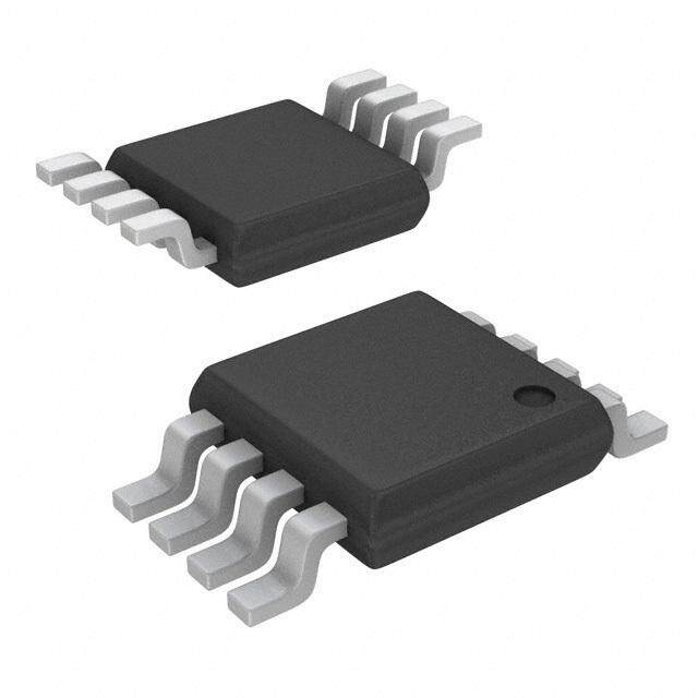
| 描述 | IC AMP AUDIO PWR 1.15W AB 16SOIC |
| 产品分类 | |
| 品牌 | Texas Instruments |
| 数据手册 | |
| 产品图片 |
|
| 产品型号 | LM4860M |
| rohs | 含铅 / 不符合限制有害物质指令(RoHS)规范要求 |
| 产品系列 | Boomer® |
| 不同负载时的最大输出功率x通道数 | 1.15W x 1 @ 8 欧姆 |
| 供应商器件封装 | 16-SOIC N |
| 其它名称 | *LM4860M |
| 包装 | 管件 |
| 安装类型 | 表面贴装 |
| 封装/外壳 | 16-SOIC(0.154",3.90mm 宽) |
| 工作温度 | -20°C ~ 85°C (TA) |
| 标准包装 | 48 |
| 特性 | 关闭,热保护 |
| 电压-电源 | 2.7 V ~ 5.5 V |
| 类型 | AB 类 |
| 输出类型 | 1-通道(单声道) |


- 商务部:美国ITC正式对集成电路等产品启动337调查
- 曝三星4nm工艺存在良率问题 高通将骁龙8 Gen1或转产台积电
- 太阳诱电将投资9.5亿元在常州建新厂生产MLCC 预计2023年完工
- 英特尔发布欧洲新工厂建设计划 深化IDM 2.0 战略
- 台积电先进制程称霸业界 有大客户加持明年业绩稳了
- 达到5530亿美元!SIA预计今年全球半导体销售额将创下新高
- 英特尔拟将自动驾驶子公司Mobileye上市 估值或超500亿美元
- 三星加码芯片和SET,合并消费电子和移动部门,撤换高东真等 CEO
- 三星电子宣布重大人事变动 还合并消费电子和移动部门
- 海关总署:前11个月进口集成电路产品价值2.52万亿元 增长14.8%


PDF Datasheet 数据手册内容提取
LM4860 www.ti.com SNAS096C–AUGUST1994–REVISEDMAY2013 LM4860 Series 1W Audio Power Amplifier with Shutdown Mode CheckforSamples:LM4860 FEATURES DESCRIPTION 1 • NoOutputCouplingCapacitors,Bootstrap The LM4860 is a bridge-connected audio power 2 amplifier capable of delivering 1W of continuous Capacitors,orSnubberCircuitsareNecessary average power to an 8Ω load with less than 1% • SmallOutline(SO)Packaging THD+N over the audio spectrum from a 5V power • CompatiblewithPCPowerSupplies supply. • ThermalShutdownProtectionCircuitry Boomer audio power amplifiers were designed • Unity-GainStable specificallytoprovidehighqualityoutputpowerwitha minimal amount of external components using • ExternalGainConfigurationCapability surface mount packaging. Since the LM4860 does • TwoHeadphoneControlInputsand not require output coupling capacitors, bootstrap HeadphoneSensingOutput capacitors or snubber networks, it is optimally suited forlow-powerportablesystems. APPLICATIONS The LM4860 features an externally controlled, low- • PersonalComputers power consumption shutdown mode, as well as an • PortableConsumerProducts internal thermal shutdown protection mechanism. It also includes two headphone control inputs and a • CellularPhones headphonesenseoutputforexternalmonitoring. • Self-PoweredSpeakers The unity-gain stable LM4860 can be configured by • ToysandGames external gain setting resistors for differential gains of up to 10 without the use of external compensation KEY SPECIFICATIONS components. Higher gains may be achieved with • THD+Nat1WContinuousAverage suitablecompensation. • OutputPowerinto8Ω:1%(Max) • InstantaneousPeakOutputPower: >2W • ShutdownCurrent: 0.6μA(typ) 1 Pleasebeawarethatanimportantnoticeconcerningavailability,standardwarranty,anduseincriticalapplicationsof TexasInstrumentssemiconductorproductsanddisclaimerstheretoappearsattheendofthisdatasheet. Alltrademarksarethepropertyoftheirrespectiveowners. 2 PRODUCTIONDATAinformationiscurrentasofpublicationdate. Copyright©1994–2013,TexasInstrumentsIncorporated Products conform to specifications per the terms of the Texas Instruments standard warranty. Production processing does not necessarilyincludetestingofallparameters.
LM4860 SNAS096C–AUGUST1994–REVISEDMAY2013 www.ti.com Typical Application Figure1. TypicalAudioAmplifierApplicationCircuit Connection Diagram Figure2. SOICPackage-TopView SeePackageNumberD0016A 2 SubmitDocumentationFeedback Copyright©1994–2013,TexasInstrumentsIncorporated ProductFolderLinks:LM4860
LM4860 www.ti.com SNAS096C–AUGUST1994–REVISEDMAY2013 Thesedeviceshavelimitedbuilt-inESDprotection.Theleadsshouldbeshortedtogetherorthedeviceplacedinconductivefoam duringstorageorhandlingtopreventelectrostaticdamagetotheMOSgates. Absolute Maximum Ratings (1)(2) SupplyVoltage 6.0V StorageTemperature −65°Cto+150°C InputVoltage −0.3VtoV +0.3V DD PowerDissipation Internallylimited ESDSusceptibility (3) 3000V ESDSusceptibility (4) 250V JunctionTemperature 150°C SolderingInformation SOICPackage VaporPhase(60sec.) 215°C Infrared(15sec.) 220°C (1) AbsoluteMaximumRatingsindicatelimitsbeyondwhichdamagetothedevicemayoccur.OperatingRatingsindicateconditionsfor whichthedeviceisfunctional,butdonotensurespecificperformancelimits.ElectricalCharacteristicsstateDCandACelectrical specificationsunderparticulartestconditionswhichensurespecificperformancelimits.Thisassumesthatthedeviceiswithinthe OperatingRatings.Specificationsarenotensuredforparameterswherenolimitisgiven,however,thetypicalvalueisagoodindication ofdeviceperformance. (2) IfMilitary/Aerospacespecifieddevicesarerequired,pleasecontacttheTexasInstrumentsSalesOffice/Distributorsforavailabilityand specifications. (3) Humanbodymodel,100pFdischargedthrougha1.5kΩresistor. (4) MachineModel,200pF–240pFdischargedthroughallpins. Operating Ratings TemperatureRange T ≤T ≤T −20°C≤T ≤+85°C MIN A MAX A SupplyVoltage 2.7V≤V ≤5.5V DD Electrical Characteristics ThefollowingspecificationsapplyforV =5V,R =8Ωunlessotherwisespecified.LimitsapplyforT =25°C. (1)(2) DD L A LM4860 Units Parameter TestConditions Typ(3) Limit(4) (Limits) V SupplyVoltage 2.7 V(min) DD 5.5 V(max) I QuiescentPowerSupplyCurrent V =0V,I =0A (5) 7.0 15.0 mA(max) DD O O I ShutdownCurrent V =V (6) 0.6 μA SD pin2 DD V OutputOffsetVoltage V =0V 5.0 50.0 mV(max) OS IN P OutputPower THD+N=1%(max);f=1kHz 1.15 1.0 W(min) O THD+N TotalHarmonicDistortion+Noise P =1Wrms;20Hz≤f≤20kHz 0.72 % O PSRR PowerSupplyRejectionRatio V =4.9Vto5.1V 65 dB DD V OutputDropoutVoltage V =0Vto5V,V =(V −V ) 0.6 1.0 V(max) od IN od o1 o2 V HP-INHighInputVoltage HP-SENSE=0Vto4V 2.5 V IH V HP-INLowInputVoltage HP-SENSE=4Vto0V 2.5 V IL V HP-SENSEHighOutputVoltage I =500μA 2.8 2.5 V(min) OH O V HP-SENSELowOutputVoltage I =−500μA 0.2 0.8 V(max) OL O (1) Allvoltagesaremeasuredwithrespecttothegroundpins,unlessotherwisespecified. (2) AbsoluteMaximumRatingsindicatelimitsbeyondwhichdamagetothedevicemayoccur.OperatingRatingsindicateconditionsfor whichthedeviceisfunctional,butdonotensurespecificperformancelimits.ElectricalCharacteristicsstateDCandACelectrical specificationsunderparticulartestconditionswhichensurespecificperformancelimits.Thisassumesthatthedeviceiswithinthe OperatingRatings.Specificationsarenotensuredforparameterswherenolimitisgiven,however,thetypicalvalueisagoodindication ofdeviceperformance. (3) Typicalsaremeasuredat25°Candrepresenttheparametricnorm. (4) LimitsarespecifiedtoTexasInstrument'sAOQL(AverageOutgoingQualityLevel). (5) Thequiescentpowersupplycurrentdependsontheoffsetvoltagewhenapracticalloadisconnectedtotheamplifier. (6) Shutdowncurrenthasawidedistribution.ForPowerManagementsensitivedesigns,contactyourlocalTexasInstrumentsSalesOffice. Copyright©1994–2013,TexasInstrumentsIncorporated SubmitDocumentationFeedback 3 ProductFolderLinks:LM4860
LM4860 SNAS096C–AUGUST1994–REVISEDMAY2013 www.ti.com High Gain Application Circuit Figure3. StereoAmplifierwithA =20 VD Single Ended Application Circuit *C andC sizedependonspecificapplicationrequirementsandconstraints.TypicalvaluesofC andC are0.1μF. S B S B **Pin2,6,or7shouldbeconnectedtoV todisabletheamplifierortoGNDtoenabletheamplifier.Thesepins DD shouldnotbeleftfloating. ***Thesecomponentscreatea“dummy”loadforpin8forstabilitypurposes. Figure4. Single-EndedAmplifierwithA =−1 V 4 SubmitDocumentationFeedback Copyright©1994–2013,TexasInstrumentsIncorporated ProductFolderLinks:LM4860
LM4860 www.ti.com SNAS096C–AUGUST1994–REVISEDMAY2013 External Components Description (SeeFigure1andFigure3) Components FunctionalDescription 1. R Invertinginputresistancewhichsetstheclosed-loopgaininconjunctionwithR.Thisresistoralsoformsahighpass i f filterwithC atf =1/(2πR C). i C i i 2. C InputcouplingcapacitorwhichblocksDCvoltageattheamplifier'sinputterminals.Alsocreatesahighpassfilter i withR atf =1/(2πR C). i C i i 3. R Feedbackresistancewhichsetsclosed-loopgaininconjunctionwithR. f i 4. C Supplybypasscapacitorwhichprovidespowersupplyfiltering.RefertoApplicationInformationforproperplacement S andselectionofsupplybypasscapacitor. 5. C Bypasspincapacitorwhichprovideshalfsupplyfiltering.RefertoApplicationInformationforproperplacementand B selectionofbypasscapacitor. 6. C(1) Usedwhenadifferentialgainofover10isdesired.C inconjunctionwithR createsalow-passfilterwhich f f f bandwidthlimitstheamplifierandpreventshighfrequencyoscillationbursts.f =1/(2πR C) C f f (1) Optionalcomponentdependentuponspecificdesignrequirements.RefertoApplicationInformationformoreinformation. Copyright©1994–2013,TexasInstrumentsIncorporated SubmitDocumentationFeedback 5 ProductFolderLinks:LM4860
LM4860 SNAS096C–AUGUST1994–REVISEDMAY2013 www.ti.com Typical Performance Characteristics THD+N THD+N vs vs Frequency Frequency Figure5. Figure6. THD+N THD+N vs vs Frequency OutputPower Figure7. Figure8. THD+N THD+N vs vs OutputPower OutputPower Figure9. Figure10. 6 SubmitDocumentationFeedback Copyright©1994–2013,TexasInstrumentsIncorporated ProductFolderLinks:LM4860
LM4860 www.ti.com SNAS096C–AUGUST1994–REVISEDMAY2013 Typical Performance Characteristics (continued) SupplyCurrent vs Time SupplyCurrentvs inShutdownMode SupplyVoltage Figure11. Figure12. LM4860NoiseFloor PowerDeratingCurve vsFrequency Figure13. Figure14. SupplyCurrentDistribution PowerDissipation vsTemperature vsOutputPower Figure15. Figure16. Copyright©1994–2013,TexasInstrumentsIncorporated SubmitDocumentationFeedback 7 ProductFolderLinks:LM4860
LM4860 SNAS096C–AUGUST1994–REVISEDMAY2013 www.ti.com Typical Performance Characteristics (continued) OutputPowervs OutputPowervs LoadResistance SupplyVoltage Figure17. Figure18. OpenLoop PowerSupply FrequencyResponse RejectionRatio Figure19. Figure20. 8 SubmitDocumentationFeedback Copyright©1994–2013,TexasInstrumentsIncorporated ProductFolderLinks:LM4860
LM4860 www.ti.com SNAS096C–AUGUST1994–REVISEDMAY2013 APPLICATION INFORMATION BRIDGE CONFIGURATION EXPLANATION As shown in Figure 1, the LM4860 has two operational amplifiers internally, allowing for a few different amplifier configurations. The first amplifier's gain is externally configurable, while the second amplifier is internally fixed in a unity-gain, inverting configuration. The closed-loop gain of the first amplifier is set by selecting the ratio of R to f R while the second amplifier's gain is fixed by the two internal 40 kΩ resistors. Figure 1 shows that the output of i amplifier one serves as the input to amplifier two which results in both amplifiers producing signals identical in magnitude,butoutofphase180°.Consequently,thedifferentialgainfortheICis: A =2*(R/R) (1) vd f i By driving the load differentially through outputs V and V , an amplifier configuration commonly referred to as O1 O2 “bridged mode” is established. Bridged mode operation is different from the classical single-ended amplifier configurationwhereonesideofitsloadisconnectedtoground. A bridge amplifier design has a few distinct advantages over the single-ended configuration, as it provides differential drive to the load, thus doubling output swing for a specified supply voltage. Consequently, four times theoutputpowerispossibleascomparedtoasingle-endedamplifierunderthesameconditions.Thisincreasein attainable output power assumes that the amplifier is not current limited or clipped. In order to choose an amplifier's closed-loop gain without causing excessive clipping which will damage high frequency transducers usedinloudspeakersystems,pleaserefertoAUDIOPOWERAMPLIFIERDESIGN. A bridge configuration, such as the one used in Boomer Audio Power Amplifiers, also creates a second advantage over single-ended amplifiers. Since the differential outputs, V and V , are biased at half-supply, no O1 O2 netDCvoltageexistsacrosstheload.Thiseliminatestheneedforanoutputcouplingcapacitorwhichisrequired in a single supply, single-ended amplifier configuration. Without an output coupling capacitor in a single supply single-ended amplifier, the half-supply bias across the load would result in both increased internal IC power dissipation and also permanent loudspeaker damage. An output coupling capacitor forms a high pass filter with the load requiring that a large value such as 470 μF be used with an 8Ω load to preserve low frequency response. This combination does not produce a flat response down to 20 Hz, but does offer a compromise betweenprintedcircuitboardsizeandsystemcost,versuslowfrequencyresponse. POWER DISSIPATION Power dissipation is a major concern when designing a successful amplifier, whether the amplifier is bridged or single-ended. A direct consequence of the increased power delivered to the load by a bridge amplifier is an increase in internal power dissipation. Equation 2 states the maximum power dissipation point for a bridge amplifieroperatingatagivensupplyvoltageanddrivingaspecifiedoutputload. P =4*(V )2/(2π2R (2) DMAX DD L) Since the LM4860 has two operational amplifiers in one package, the maximum internal power dissipation is 4 times that of a single-ended amplifier. Even with this substantial increase in power dissipation, the LM4860 does not require heatsinking. From Equation 2, assuming a 5V power supply and an 8Ω load, the maximum power dissipationpointis625mW.ThemaximumpowerdissipationpointobtainedfromEquation2mustnotbegreater thanthepowerdissipationthatresultsfromEquation3: P =(T −T )/θ (3) DMAX JMAX A JA For the LM4860 surface mount package, θ = 100°C/W and T = 150°C. Depending on the ambient JA JMAX temperature, T , of the system surroundings, Equation 3 can be used to find the maximum internal power A dissipation supported by the IC packaging. If the result of Equation 2 is greater than that of Equation 3, then either the supply voltage must be decreased or the load impedance increased. For the typical application of a 5V power supply, with an 8Ω load, the maximum ambient temperature possible without violating the maximum junction temperature is approximately 88°C, provided that device operation is around the maximum power dissipation point. Power dissipation is a function of output power and thus, if typical operation is not around the maximum power dissipation point, the ambient temperature can be increased. Refer to Typical Performance Characteristicsforpowerdissipationinformationforloweroutputpowers. Copyright©1994–2013,TexasInstrumentsIncorporated SubmitDocumentationFeedback 9 ProductFolderLinks:LM4860
LM4860 SNAS096C–AUGUST1994–REVISEDMAY2013 www.ti.com POWER SUPPLY BYPASSING As with any power amplifier, proper supply bypassing is critical for low noise performance and high power supply rejection. The capacitor location on both the bypass and power supply pins should be as close to the device as possible. As displayed in Typical Performance Characteristics, the effect of a larger half-supply bypass capacitor is improved low frequency THD+N due to increased half-supply stability. Typical applications employ a 5V regulator with 10 μF and a 0.1 μF bypass capacitors which aid in supply stability, but do not eliminate the need for bypassing the supply nodes of the LM4860. The selection of bypass capacitors, especially C , is thus B dependantupondesiredlowfrequencyTHD+N,systemcost,andsizeconstraints. SHUTDOWN FUNCTION Inordertoreducepowerconsumptionwhilenotinuse,theLM4860containsashutdownpintoexternallyturnoff the amplifier's bias circuitry. The shutdown feature turns the amplifier off when a logic high is placed on the shutdown pin. Upon going into shutdown, the output is immediately disconnected from the speaker. There is a built-in threshold which produces a drop in quiescent current to 500 μA typically. For a 5V power supply, this threshold occurs when 2V–3V is applied to the shutdown pin. A typical quiescent current of 0.6 μA results when the supply voltage is applied to the shutdown pin. In many applications, a microcontroller or microprocessor output is used to control the shutdown circuitry which provides a quick, smooth transition into shutdown. Another solution is to use a single-pole, single-throw switch that when closed, is connected to ground and enables the amplifier. If the switch is open, then a soft pull-up resistor of 47 kΩ will disable the LM4860. There are no soft pull-down resistors inside the LM4860, so a definite shutdown pin voltage must be applied externally, or the internallogicgatewillbeleftfloatingwhichcoulddisabletheamplifierunexpectedly. HEADPHONE CONTROL INPUTS TheLM4860possessestwoheadphonecontrolinputsthatdisabletheamplifierandreduceI tolessthan1mA DD wheneitheroneorbothoftheseinputshavealogic-highvoltageplacedontheirpins. Unlike the shutdown function, the headphone control function does not provide the level of current conservation that is required for battery powered systems. Since the quiescent current resulting from the headphone control function is 1000 times more than the shutdown function, the residual currents in the device may create a pop at theoutputwhencomingoutoftheheadphonecontrolmode.Thepopeffectmaybeeliminatedbyconnectingthe headphone sensing output to the shutdown pin input as shown in Figure 21. This solution will not only eliminate the output pop, but will also utilize the full current conservation of the shutdown function by reducing I to DD 0.6 μA. The amplifier will then be fully shutdown. This configuration also allows the designer to use the control inputs as either two headphone control pins or a headphone control pin and a shutdown pin where the lowest levelofcurrentconsumptionisobtainedfromeitherfunction. Figure 22 shows the implementation of the LM4860's headphone control function using a single-supply headphone amplifier. The voltage divider of R1 and R2 sets the voltage at the HP-IN1 pin to be approximately 50 mV when there are no headphones plugged into the system. This logic-low voltage at the HP-IN1 pin enables the LM4860 to amplify AC signals. Resistor R3 limits the amount of current flowing out of the HP-IN1 pin when the voltage at that pin goes below ground resulting from the music coming from the headphone amplifier. The output coupling cap protects the headphones by blocking the amplifier's half-supply DC voltage. The capacitor also protects the headphone amplifier from the low voltage set up by resistors R1 and R2 when there aren't any headphones plugged into the system. The tricky point to this setup is that the AC output voltage of the headphone amplifier cannot exceed the 2.0V HP-IN1 voltage threshold when there aren't any headphones plugged into the system, assuming that R1 and R2 are 100k and 1k, respectively. The LM4860 may not be fully shutdown when this level is exceeded momentarily, due to the discharging time constant of the bias-pin voltage. Thistimeconstantisestablishedbythetwo50kresistors(inparallel)withtheseriesbypasscapacitorvalue. When a set of headphones are plugged into the system, the contact pin of the headphone jack is disconnected from the signal pin, interrupting the voltage divider set up by resistors R1 and R2. Resistor R1 then pulls up the HP-IN1 pin, enabling the headphone function and disabling the LM4860 amplifier. The headphone amplifier then drives the headphones, whose impedance is in parallel with resistor R2. Since the typical impedance of headphonesare32Ω,resistorR2hasnegligibleeffectontheoutputdrivecapability.AlsoshowninFigure22are the electrical connections for the headphone jack and plug. A 3-wire plug consists of a Tip, Ring, and Sleave, where the Tip and Ring are signal carrying conductors and the Sleave is the common ground return. One control pincontactforeachheadphonejackissufficienttoindicatetocontrolinputsthattheuserhasinsertedapluginto ajackandthatanothermodeofoperationisdesired. 10 SubmitDocumentationFeedback Copyright©1994–2013,TexasInstrumentsIncorporated ProductFolderLinks:LM4860
LM4860 www.ti.com SNAS096C–AUGUST1994–REVISEDMAY2013 Forasystemimplementationwheretheheadphoneamplifierisdesignedusingasplitsupply,theoutputcoupling cap, C and resistor R2 of Figure 22, can be eliminated. The functionality described earlier remains the same, C however. In addition, the HP-SENSE pin, although it may be connected to the SHUTDOWN pin as shown in Figure 21, may still be used as a control flag. It is capable of driving the input to another logic gate or approximately 2 mA withoutseriousloading. Figure21. HP-SENSEPinto SHUTDOWNPinConnection Figure22. TypicalHeadphoneControlInputCircuitry Copyright©1994–2013,TexasInstrumentsIncorporated SubmitDocumentationFeedback 11 ProductFolderLinks:LM4860
LM4860 SNAS096C–AUGUST1994–REVISEDMAY2013 www.ti.com HIGHER GAIN AUDIO AMPLIFIER The LM4860 is unity-gain stable and requires no external components besides gain-setting resistors, an input coupling capacitor, and proper supply bypassing in the typical application. However if a closed-loop differential gain of greater than 10 is required, then a feedback capacitor is needed, as shown in Figure 3, to bandwidth limit the amplifier. The feedback capacitor creates a low pass filter that eliminates unwanted high frequency oscillations. Care should be taken when calculating the −3 dB frequency in that an incorrect combination of R f and C will cause rolloff before 20 kHz. A typical combination of feedback resistor and capacitor that will not f produce audio band high frequency rolloff is R = 100 kΩ and C = 5 pF. These components result in a −3 dB f f point of approximately 320 kHz. Once the differential gain of the amplifier has been calculated, a choice of R will f result,andC canthenbecalculatedfromtheformulastatedinExternalComponentsDescription. f VOICE-BAND AUDIO AMPLIFIER Many applications, such as telephony, only require a voice-band frequency response. Such an application usually requires a flat frequency response from 300 Hz to 3.5 kHz. By adjusting the component values of Figure 3, this common application requirement can be implemented. The combination of R and C form a i i highpass filter while R and C form a lowpass filter. Using the typical voice-band frequency range, with a f f passband differential gain of approximately 100, the following values of R, C, R, and C follow from the i i f f equationsstatedinExternalComponentsDescription. R =10kΩ, R =510k, C =0.22μF, and C =15pF (4) i f i f Five times away from a −3 dB point is 0.17 dB down from the flatband response. With this selection of components, the resulting −3 dB points, f and f , are 72 Hz and 20 kHz, respectively, resulting in a flatband L H frequency response of better than ±0.25 dB with a rolloff of 6 dB/octave outside of the passband. If a steeper rolloffisrequired,othercommonbandpassfilteringtechniquescanbeusedtoachievehigherorderfilters. SINGLE-ENDED AUDIO AMPLIFIER Although the typical application for the LM4860 is a bridged monoaural amp, it can also be used to drive a load single-endedly in applications, such as PC cards, which require that one side of the load is tied to ground. Figure 4 shows a common single-ended application, where V is used to drive the speaker. This output is O1 coupledthrougha470μFcapacitor,whichblocksthehalf-supplyDCbiasthatexistsinallsingle-supplyamplifier configurations. This capacitor, designated C in Figure 4, in conjunction with R , forms a highpass filter. The O L −3dBpointofthishighpassfilteris1/(2πR C ),socareshouldbetakentomakesurethattheproductofR and L O L C is large enough to pass low frequencies to the load. When driving an 8Ω load, and if a full audio spectrum O reproduction is required, C should be at least 470 μF. V , the output that is not used, is connected through a O O2 0.1 μF capacitor to a 2 kΩ load to prevent instability. While such an instability will not affect the waveform of V , O1 itisgooddesignpracticetoloadthesecondoutput. AUDIO POWER AMPLIFIER DESIGN Designa500mW/8ΩAudioAmplifier Given: PowerOutput: 500mWrms LoadImpedance: 8Ω InputLevel: 1Vrms(max) InputImpedance: 20kΩ Bandwidth: 20Hz-20kHz±0.25dB A designer must first determine the needed supply rail to obtain the specified output power. Calculating the required supply rail involves knowing two parameters, V and also the dropout voltage. The latter is typically opeak 0.7V.V canbedeterminedfromEquation5. opeak V 2 R P opeak L O (5) 12 SubmitDocumentationFeedback Copyright©1994–2013,TexasInstrumentsIncorporated ProductFolderLinks:LM4860
LM4860 www.ti.com SNAS096C–AUGUST1994–REVISEDMAY2013 For500mWofoutputpowerintoan8Ω load,therequiredV is2.83V.Aminimumsupplyrailof3.53Vresults opeak from adding V and V . But 3.53V is not a standard voltage that exists in many applications and for this opeak od reason, a supply rail of 5V is designated. Extra supply voltage creates dynamic headroom that allows the LM4860 to reproduce peaks in excess of 500 mW without clipping the signal. At this time, the designer must make sure that the power supply choice along with the output impedance does not violate the conditions explainedinPOWERDISSIPATION. Once the power dissipation equations have been addressed, the required differential gain can be determined fromEquation6. A t 2(cid:13) (cid:11)P R (cid:12) / (cid:11)V (cid:12) V / V vd O L IN orms inrms (6) FromEquation6,theminimumA is: A =2 vd vd Since the desired input impedance was 20 kΩ, and with an A of 2, a ratio of 1:1 of R to Rresults in an vd f i allocation of R = R = 20 kΩ. Since the A was less than 10, a feedback capacitor is not needed. The final i f vd design step is to address the bandwidth requirements which must be stated as a pair of −3 dB frequency points. Five times away from a −3 dB point is 0.17 dB down from passband response which is better than the required ±0.25 dB specified. This fact results in a low and high frequency pole of 4 Hz and 100 kHz respectively. As statedinExternalComponentsDescription,R inconjunctionwithC createahighpassfilter. i i C ≥1/(2π*20kΩ*4Hz)=1.98μF; use2.2μF. (7) i The high frequency pole is determined by the product of the desired high frequency pole, f , and the differential H gain, A . With a A = 2 and f = 100 kHz, the resulting GBWP = 100 kHz which is much smaller than the vd vd H LM4860 GBWP of 7 MHz. This figure displays that if a designer has a need to design an amplifier with a higher differentialgain,theLM4860canstillbeusedwithoutrunningintobandwidthproblems. Copyright©1994–2013,TexasInstrumentsIncorporated SubmitDocumentationFeedback 13 ProductFolderLinks:LM4860
LM4860 SNAS096C–AUGUST1994–REVISEDMAY2013 www.ti.com REVISION HISTORY ChangesfromRevisionB(May2013)toRevisionC Page • ChangedlayoutofNationalDataSheettoTIformat.......................................................................................................... 13 14 SubmitDocumentationFeedback Copyright©1994–2013,TexasInstrumentsIncorporated ProductFolderLinks:LM4860
PACKAGE OPTION ADDENDUM www.ti.com 6-Feb-2020 PACKAGING INFORMATION Orderable Device Status Package Type Package Pins Package Eco Plan Lead/Ball Finish MSL Peak Temp Op Temp (°C) Device Marking Samples (1) Drawing Qty (2) (6) (3) (4/5) LM4860M ACTIVE SOIC D 16 48 TBD Call TI Call TI -20 to 85 LM4860M LM4860M/NOPB ACTIVE SOIC D 16 48 Green (RoHS SN Level-1-260C-UNLIM -20 to 85 LM4860M & no Sb/Br) LM4860MX/NOPB ACTIVE SOIC D 16 2500 Green (RoHS SN Level-1-260C-UNLIM -20 to 85 LM4860M & no Sb/Br) (1) The marketing status values are defined as follows: ACTIVE: Product device recommended for new designs. LIFEBUY: TI has announced that the device will be discontinued, and a lifetime-buy period is in effect. NRND: Not recommended for new designs. Device is in production to support existing customers, but TI does not recommend using this part in a new design. PREVIEW: Device has been announced but is not in production. Samples may or may not be available. OBSOLETE: TI has discontinued the production of the device. (2) RoHS: TI defines "RoHS" to mean semiconductor products that are compliant with the current EU RoHS requirements for all 10 RoHS substances, including the requirement that RoHS substance do not exceed 0.1% by weight in homogeneous materials. Where designed to be soldered at high temperatures, "RoHS" products are suitable for use in specified lead-free processes. TI may reference these types of products as "Pb-Free". RoHS Exempt: TI defines "RoHS Exempt" to mean products that contain lead but are compliant with EU RoHS pursuant to a specific EU RoHS exemption. Green: TI defines "Green" to mean the content of Chlorine (Cl) and Bromine (Br) based flame retardants meet JS709B low halogen requirements of <=1000ppm threshold. Antimony trioxide based flame retardants must also meet the <=1000ppm threshold requirement. (3) MSL, Peak Temp. - The Moisture Sensitivity Level rating according to the JEDEC industry standard classifications, and peak solder temperature. (4) There may be additional marking, which relates to the logo, the lot trace code information, or the environmental category on the device. (5) Multiple Device Markings will be inside parentheses. Only one Device Marking contained in parentheses and separated by a "~" will appear on a device. If a line is indented then it is a continuation of the previous line and the two combined represent the entire Device Marking for that device. (6) Lead/Ball Finish - Orderable Devices may have multiple material finish options. Finish options are separated by a vertical ruled line. Lead/Ball Finish values may wrap to two lines if the finish value exceeds the maximum column width. Important Information and Disclaimer:The information provided on this page represents TI's knowledge and belief as of the date that it is provided. TI bases its knowledge and belief on information provided by third parties, and makes no representation or warranty as to the accuracy of such information. Efforts are underway to better integrate information from third parties. TI has taken and continues to take reasonable steps to provide representative and accurate information but may not have conducted destructive testing or chemical analysis on incoming materials and chemicals. TI and TI suppliers consider certain information to be proprietary, and thus CAS numbers and other limited information may not be available for release. Addendum-Page 1
PACKAGE OPTION ADDENDUM www.ti.com 6-Feb-2020 In no event shall TI's liability arising out of such information exceed the total purchase price of the TI part(s) at issue in this document sold by TI to Customer on an annual basis. Addendum-Page 2
PACKAGE MATERIALS INFORMATION www.ti.com 24-Aug-2017 TAPE AND REEL INFORMATION *Alldimensionsarenominal Device Package Package Pins SPQ Reel Reel A0 B0 K0 P1 W Pin1 Type Drawing Diameter Width (mm) (mm) (mm) (mm) (mm) Quadrant (mm) W1(mm) LM4860MX/NOPB SOIC D 16 2500 330.0 16.4 6.5 10.3 2.3 8.0 16.0 Q1 PackMaterials-Page1
PACKAGE MATERIALS INFORMATION www.ti.com 24-Aug-2017 *Alldimensionsarenominal Device PackageType PackageDrawing Pins SPQ Length(mm) Width(mm) Height(mm) LM4860MX/NOPB SOIC D 16 2500 367.0 367.0 35.0 PackMaterials-Page2
None
IMPORTANTNOTICEANDDISCLAIMER TI PROVIDES TECHNICAL AND RELIABILITY DATA (INCLUDING DATASHEETS), DESIGN RESOURCES (INCLUDING REFERENCE DESIGNS), APPLICATION OR OTHER DESIGN ADVICE, WEB TOOLS, SAFETY INFORMATION, AND OTHER RESOURCES “AS IS” AND WITH ALL FAULTS, AND DISCLAIMS ALL WARRANTIES, EXPRESS AND IMPLIED, INCLUDING WITHOUT LIMITATION ANY IMPLIED WARRANTIES OF MERCHANTABILITY, FITNESS FOR A PARTICULAR PURPOSE OR NON-INFRINGEMENT OF THIRD PARTY INTELLECTUAL PROPERTY RIGHTS. These resources are intended for skilled developers designing with TI products. You are solely responsible for (1) selecting the appropriate TI products for your application, (2) designing, validating and testing your application, and (3) ensuring your application meets applicable standards, and any other safety, security, or other requirements. These resources are subject to change without notice. TI grants you permission to use these resources only for development of an application that uses the TI products described in the resource. Other reproduction and display of these resources is prohibited. No license is granted to any other TI intellectual property right or to any third party intellectual property right. TI disclaims responsibility for, and you will fully indemnify TI and its representatives against, any claims, damages, costs, losses, and liabilities arising out of your use of these resources. TI’s products are provided subject to TI’s Terms of Sale (www.ti.com/legal/termsofsale.html) or other applicable terms available either on ti.com or provided in conjunction with such TI products. TI’s provision of these resources does not expand or otherwise alter TI’s applicable warranties or warranty disclaimers for TI products. Mailing Address: Texas Instruments, Post Office Box 655303, Dallas, Texas 75265 Copyright © 2020, Texas Instruments Incorporated