ICGOO在线商城 > 集成电路(IC) > PMIC - 电压基准 > LM4050BIM3-2.5/NOPB

 Datasheet下载
- 型号: LM4050BIM3-2.5/NOPB
- 制造商: Texas Instruments
- 库位|库存: xxxx|xxxx
- 要求:
| 数量阶梯 | 香港交货 | 国内含税 |
| +xxxx | $xxxx | ¥xxxx |
查看当月历史价格
查看今年历史价格
LM4050BIM3-2.5/NOPB产品简介:
ICGOO电子元器件商城为您提供LM4050BIM3-2.5/NOPB由Texas Instruments设计生产,在icgoo商城现货销售,并且可以通过原厂、代理商等渠道进行代购。 LM4050BIM3-2.5/NOPB价格参考¥6.40-¥14.41。Texas InstrumentsLM4050BIM3-2.5/NOPB封装/规格:PMIC - 电压基准, Shunt Voltage Reference IC ±0.2% 15mA SOT-23-3。您可以下载LM4050BIM3-2.5/NOPB参考资料、Datasheet数据手册功能说明书,资料中有LM4050BIM3-2.5/NOPB 详细功能的应用电路图电压和使用方法及教程。
LM4050BIM3-2.5/NOPB是德州仪器(Texas Instruments)生产的一款精密电压基准芯片,属于PMIC中的电压基准类别。该器件提供稳定的2.5V输出电压,具有低静态电流、高精度和良好的温度稳定性,适用于对电源精度要求较高的场合。

其典型应用场景包括便携式设备(如智能手机、平板电脑)、电池供电系统、数据采集系统、模数转换器(ADC)和数模转换器(DAC)的参考电压源。在工业测量仪器、传感器信号调理电路以及医疗电子设备中,该芯片可确保高精度模拟信号处理的稳定性与可靠性。

此外,LM4050BIM3-2.5/NOPB采用SOT-23小型封装,节省空间,适合高密度PCB布局;其“NOPB”标识表示无铅环保设计,符合RoHS标准,广泛应用于消费电子、工业控制和汽车电子等领域。由于具备出色的长期稳定性和低噪声特性,它也常用于需要长时间可靠运行的监控与通信设备中。总之,这款电压基准芯片凭借其高性能和紧凑设计,成为多种精密电子系统中的关键元件。
| 参数 | 数值 |
| 产品目录 | 集成电路 (IC)半导体 |
| 描述 | IC VREF SHUNT PREC 2.5V SOT23-3参考电压 PREC MICROPWR SHUNT VLTG REF |
| 产品分类 | |
| 品牌 | Texas Instruments |
| 产品手册 | |
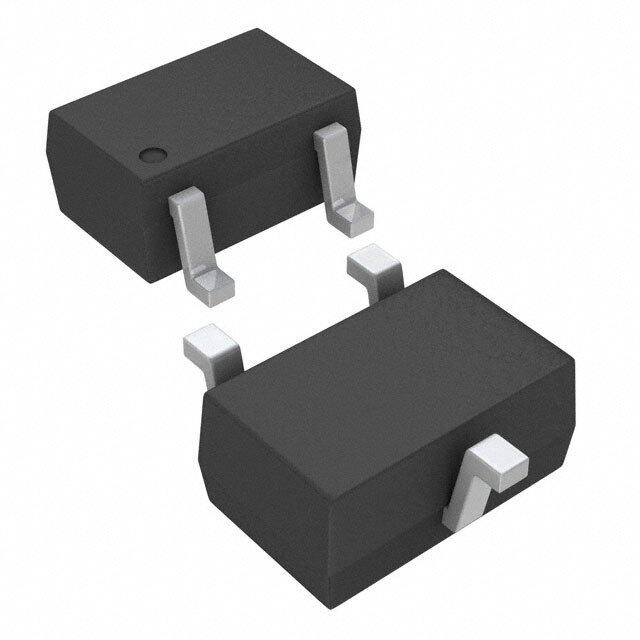
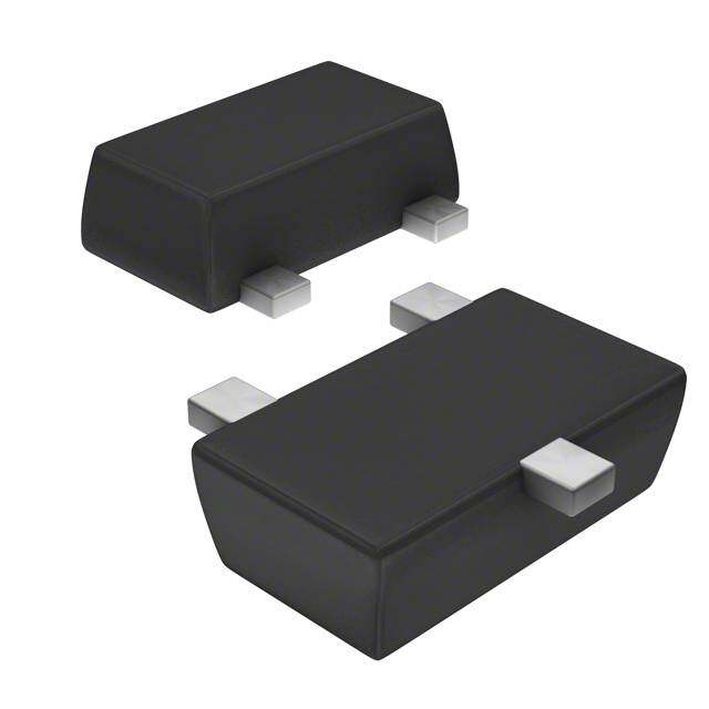
| 产品图片 |
|
| rohs | 符合RoHS无铅 / 符合限制有害物质指令(RoHS)规范要求 |
| 产品系列 | 电源管理 IC,参考电压,Texas Instruments LM4050BIM3-2.5/NOPB- |
| 数据手册 | |
| 产品型号 | LM4050BIM3-2.5/NOPB |
| 串联VREF—输入电压—最大值 | 2.5 V |
| 产品培训模块 | http://www.digikey.cn/PTM/IndividualPTM.page?site=cn&lang=zhs&ptm=26100 |
| 产品目录页面 | |
| 产品种类 | 参考电压 |
| 供应商器件封装 | SOT-23-3 |
| 其它名称 | *LM4050BIM3-2.5/NOPB |
| 分流电流—最大值 | 15 mA |
| 初始准确度 | 0.2 % |
| 制造商产品页 | http://www.ti.com/general/docs/suppproductinfo.tsp?distId=10&orderablePartNumber=LM4050BIM3-2.5/NOPB |
| 包装 | 剪切带 (CT) |
| 参考类型 | 旁路,精度 |
| 商标 | Texas Instruments |
| 安装类型 | 表面贴装 |
| 安装风格 | SMD/SMT |
| 容差 | ±0.2% |
| 封装 | Reel |
| 封装/外壳 | TO-236-3,SC-59,SOT-23-3 |
| 封装/箱体 | SOT-23 |
| 工作温度 | -40°C ~ 85°C |
| 工厂包装数量 | 1000 |
| 平均温度系数—典型值 | 20 PPM/C (Typ) |
| 最大工作温度 | + 85 C |
| 最小工作温度 | - 40 C |
| 标准包装 | 1 |
| 温度系数 | 50ppm/°C |
| 电压-输入 | - |
| 电压-输出 | 2.5V |
| 电流-输出 | 15mA |
| 电流-阴极 | 60µA |
| 电流-静态 | - |
| 系列 | LM4050-N |
| 输出电压 | 2.5 V |
| 通道数 | 1 |


- 商务部:美国ITC正式对集成电路等产品启动337调查
- 曝三星4nm工艺存在良率问题 高通将骁龙8 Gen1或转产台积电
- 太阳诱电将投资9.5亿元在常州建新厂生产MLCC 预计2023年完工
- 英特尔发布欧洲新工厂建设计划 深化IDM 2.0 战略
- 台积电先进制程称霸业界 有大客户加持明年业绩稳了
- 达到5530亿美元!SIA预计今年全球半导体销售额将创下新高
- 英特尔拟将自动驾驶子公司Mobileye上市 估值或超500亿美元
- 三星加码芯片和SET,合并消费电子和移动部门,撤换高东真等 CEO
- 三星电子宣布重大人事变动 还合并消费电子和移动部门
- 海关总署:前11个月进口集成电路产品价值2.52万亿元 增长14.8%


PDF Datasheet 数据手册内容提取
Product Sample & Technical Tools & Support & Folder Buy Documents Software Community LM4050-N,LM4050-N-Q1 SNOS455G–MAY2000–REVISEDSEPTEMBER2015 LM4050-N/-Q1 Precision Micropower Shunt Voltage Reference 1 Features 3 Description • SmallPackage:SOT-23 Ideal for space-critical applications, the LM4050-N 1 precision voltage reference is available in the sub- • NoOutputCapacitorRequired miniature (3 mm × 1.3 mm) SOT-23 surface-mount • ToleratesCapacitiveLoads package. The LM4050-N design eliminates the need • FixedReverseBreakdownVoltagesof2.048V, for an external stabilizing capacitor while ensuring 2.5V,4.096V,5V,8.192V,and10V stability with any capacitive load, thus making the LM4050-N easy to use. Further reducing design effort • KeySpecifications(LM4050-N) is the availability of several fixed reverse breakdown – OutputVoltageTolerance(AGrade,25°C) voltages: 2.048 V, 2.5 V, 4.096 V, 5 V, 8.192 V, and ±0.1%(Maximum) 10 V. The minimum operating current increases from – LowOutputNoise(10Hzto10kHz)41 μVrms 60 μA for the LM4050-N-2.0 to 100 μA for the LM4050-N-10.0. All versions have a maximum (Typical) operatingcurrentof15mA. – WideOperatingCurrentRange60 μAto15 mA The LM4050-N utilizes fuse and Zener-zap reverse breakdown voltage trim during wafer sort to ensure – IndustrialTemperatureRange −40°Cto85°C that the prime parts have an accuracy of better than – ExtendedTemperatureRange −40°Cto125°C ±0.1% (A grade) at 25°C. Bandgap reference – LowTemperatureCoefficient50ppm/°C(max) temperature drift curvature correction and low dynamic impedance ensure stable reverse – LM4050-N-Q1isAEC-Q100Grade1Qualified breakdown voltage accuracy over a wide range of andareManufacturedonanAutomotive operatingtemperaturesandcurrents. GradeFlow All grades and voltage options of the LM4050-N are 2 Applications available in both an industrial temperature range (−40°C and 85°C) and an extended temperature • Portable,Battery-PoweredEquipment range(−40°Cand125°C). • DataAcquisitionSystems DeviceInformation(1) • Instrumentation • ProcessControl PARTNUMBER PACKAGE BODYSIZE(NOM) LM4050-N • EnergyManagement SOT-23(3) 2.92mm×1.30mm LM4050-N-Q1 • ProductTesting (1) For all available packages, see the orderable addendum at • Automotive theendofthedatasheet. • PrecisionAudioComponents ShuntRegulatorSchematic I +I Q L I L Vs Vout Rs Cathode I Q Cout Anode 1 An IMPORTANT NOTICE at the end of this data sheet addresses availability, warranty, changes, use in safety-critical applications, intellectualpropertymattersandotherimportantdisclaimers.PRODUCTIONDATA.
LM4050-N,LM4050-N-Q1 SNOS455G–MAY2000–REVISEDSEPTEMBER2015 www.ti.com Table of Contents 1 Features.................................................................. 1 8.1 Overview.................................................................13 2 Applications........................................................... 1 8.2 FunctionalBlockDiagram.......................................13 3 Description............................................................. 1 8.3 FeatureDescription.................................................13 8.4 DeviceFunctionalModes........................................13 4 RevisionHistory..................................................... 2 9 ApplicationandImplementation........................ 14 5 PinConfigurationandFunctions......................... 3 9.1 ApplicationInformation............................................14 6 Specifications......................................................... 3 9.2 TypicalApplications................................................15 6.1 AbsoluteMaximumRatings......................................3 10 PowerSupplyRecommendations..................... 21 6.2 ESDRatings..............................................................3 11 Layout................................................................... 21 6.3 RecommendedOperatingConditions......................4 6.4 ThermalInformation..................................................4 11.1 LayoutGuidelines.................................................21 6.5 ElectricalCharacteristics:2-VOption.......................5 11.2 LayoutExample....................................................21 6.6 ElectricalCharacteristics:2.5-VOption....................6 12 DeviceandDocumentationSupport................. 22 6.7 ElectricalCharacteristics:4.1-VOption....................7 12.1 RelatedLinks........................................................22 6.8 ElectricalCharacteristics:5-VOption ......................8 12.2 CommunityResources..........................................22 6.9 ElectricalCharacteristics:8.2-VOption ...................9 12.3 Trademarks...........................................................22 6.10 ElectricalCharacteristics:10-VOption ................10 12.4 ElectrostaticDischargeCaution............................22 6.11 TypicalCharacteristics..........................................11 12.5 Glossary................................................................22 7 ParameterMeasurementInformation................12 13 Mechanical,Packaging,andOrderable Information........................................................... 22 8 DetailedDescription............................................ 13 4 Revision History NOTE:Pagenumbersforpreviousrevisionsmaydifferfrompagenumbersinthecurrentversion. ChangesfromRevisionF(June2015)toRevisionG Page • AddedESDRatingstable,FeatureDescriptionsection,DeviceFunctionalModes,ApplicationandImplementation section,PowerSupplyRecommendationssection,Layoutsection,DeviceandDocumentationSupportsection,and Mechanical,Packaging,andOrderableInformationsection.................................................................................................. 1 • RemovedVaporPhaseandInfraredLeadTemperaturesfromAbsMaxRatingstable. ...................................................... 3 ChangesfromRevisionE(April2013)toRevisionF Page • Deleted"-25"from(LM4050-N)inKeySpecificationstitleand"A/-Q1B/-Q1C"fromKeySpecificationre:autograde........1 • AddedMaximumJunctionTemperaturetoAbsMaxRatingstable ...................................................................................... 3 • AddedtablenotestoOperatingRatingstabletoclarifyoperatingandhighjunctiontemperatureranges............................ 4 • Deleted"-N"frompartnumbersinECtable"Limits"columnheaders .................................................................................. 5 ChangesfromRevisionD(April2013)toRevisionE Page • ChangedlayoutofNationalDataSheettoTIformat........................................................................................................... 20 2 SubmitDocumentationFeedback Copyright©2000–2015,TexasInstrumentsIncorporated ProductFolderLinks:LM4050-N LM4050-N-Q1
LM4050-N,LM4050-N-Q1 www.ti.com SNOS455G–MAY2000–REVISEDSEPTEMBER2015 5 Pin Configuration and Functions DBZPackage 3-PinSOT-23 TopView *Thispinmustbeleftfloatingorconnectedtopin2. PinFunctions PIN I/O DESCRIPTION NAME NO. Cathode 1 I/O Shuntcurrentandinputvoltage Anode 2 O Commonpin,normallyconnectedtoground NC 3 — Nointernalconnection 6 Specifications 6.1 Absolute Maximum Ratings See (1),(2) MIN MAX UNIT ReverseCurrent 20 mA ForwardCurrent 10 mA PowerDissipation(T =25°C)(3) 280 mW A MaximumJunctionTemperature (4) 150 °C StorageTemperature –65 150 °C (1) StressesbeyondthoselistedunderAbsoluteMaximumRatingsmaycausepermanentdamagetothedevice.Thesearestressratings only,whichdonotimplyfunctionaloperationofthedeviceattheseoranyotherconditionsbeyondthoseindicatedunderRecommended OperatingConditions.Exposuretoabsolute-maximum-ratedconditionsforextendedperiodsmayaffectdevicereliability. (2) IfMilitary/Aerospacespecifieddevicesarerequired,pleasecontacttheTexasInstrumentsSalesOffice/Distributorsforavailabilityand specifications. (3) ThemaximumpowerdissipationmustbederatedatelevatedtemperaturesandisdictatedbyT (maximumjunctiontemperature), Jmax R (junctiontoambientthermalresistance),andT (ambienttemperature).Themaximumallowablepowerdissipationatany θJA A temperatureisPD =(T −T )/R orthenumbergivenintheAbsoluteMaximumRatings,whicheverislower.FortheLM4050-N, max Jmax A θJA T =150°C,andthetypicalthermalresistance(R ),whenboardmounted,is326°C/WfortheSOT-23package. Jmax θJA (4) Highjunctiontemperaturesdegradeoperatinglifetimes.Operatinglifetimeisde-ratedforjunctiontemperaturesgreaterthan125°C. 6.2 ESD Ratings VALUE UNIT Humanbodymodel(HBM),perANSI/ESDA/JEDECJS-001(1) ±2000 V Electrostatic Chargeddevicemodel(CDM),perJEDECspecificationJESD22-C101(2) ±1000 V (ESD) discharge Machinemodel(MM) ±200 (1) JEDECdocumentJEP155statesthat500-VHBMallowssafemanufacturingwithastandardESDcontrolprocess. (2) JEDECdocumentJEP157statesthat250-VCDMallowssafemanufacturingwithastandardESDcontrolprocess. Copyright©2000–2015,TexasInstrumentsIncorporated SubmitDocumentationFeedback 3 ProductFolderLinks:LM4050-N LM4050-N-Q1
LM4050-N,LM4050-N-Q1 SNOS455G–MAY2000–REVISEDSEPTEMBER2015 www.ti.com 6.3 Recommended Operating Conditions overoperatingfree-airtemperaturerange(unlessotherwisenoted) (1)(2) MIN MAX UNIT AmbientTemperatureRange –40 85 °C IndustrialTemperatureRange JunctionTemperatureRange –40 85 °C AmbientTemperatureRange –40 125 °C ExtendedTemperatureRange JunctionTemperature –40 125 °C (1) ThemaximumpowerdissipationmustbederatedatelevatedtemperaturesandisdictatedbyT (maximumjunctiontemperature), Jmax R (junctiontoambientthermalresistance),andT (ambienttemperature).Themaximumallowablepowerdissipationatany θJA A temperatureisPD =(T −T )/R orthenumbergivenintheAbsoluteMaximumRatings,whicheverislower.FortheLM4050-N, max Jmax A θJA T =150°C,andthetypicalthermalresistance(R ),whenboardmounted,is326°C/WfortheSOT-23package. Jmax θJA (2) RecommendedOperatingConditionsareconditionsunderthedeviceisintendedtobefunctional.Forspecificationsandconditions,see ElectricalCharacteristicssection. 6.4 Thermal Information LM4050-N/-Q1 THERMALMETRIC(1) DBZ(SOT-23) UNIT 3PINS R Junction-to-ambientthermalresistance 287 °C/W θJA R Junction-to-case(top)thermalresistance 106.6 °C/W θJC(top) R Junction-to-boardthermalresistance 57.7 °C/W θJB ψ Junction-to-topcharacterizationparameter 5.5 °C/W JT ψ Junction-to-boardcharacterizationparameter 56.4 °C/W JB R Junction-to-case(bottom)thermalresistance N/A °C/W θJC(bot) (1) Formoreinformationabouttraditionalandnewthermalmetrics,seetheSemiconductorandICPackageThermalMetricsapplication report,SPRA953. 4 SubmitDocumentationFeedback Copyright©2000–2015,TexasInstrumentsIncorporated ProductFolderLinks:LM4050-N LM4050-N-Q1
LM4050-N,LM4050-N-Q1 www.ti.com SNOS455G–MAY2000–REVISEDSEPTEMBER2015 6.5 Electrical Characteristics: 2-V Option AllotherlimitsT =T =25°C.ThegradesA,BandCdesignateinitialReverseBreakdownVoltagetolerancesof±0.1%, A J ±0.2%,and0.5%respectively. PARAMETER TESTCONDITIONS MIN(1) TYP(2) MAX(1) UNIT ReverseBreakdownVoltage IR=100μA 2.048 V LM4050AIM3,LM4050AEM3 ±2.048 IR=100μA LM4050BIM3,LM4050BEM3 ±4.096 LM4050CIM3,LM4050CEM3 ±1024 LM4050AIM3,LM4050AEM3 ±9.0112 VR Reversebreakdownvoltage Industrialtemperaturerange tolerance(3) TA=TJ=TMINtoTMAX LM4050BIM3,LM4050BEM3 ±11.4688 mV LM4050CIM3,LM4050CEM3 ±14.7456 LM4050AIM3,LM4050AEM3 ±12.288 Extendedtemperaturerange LM4050BIM3,LM4050BEM3 ±14.7456 TA=TJ=TMINtoTMAX LM4050CIM3,LM4050CEM3 ±17.2032 TA=TJ=25°C 41 60 IRMIN Minimumoperatingcurrent μA TA=TJ=TMINtoTMAX 65 IR=10mA ±20 Averagereversebreakdown IR=1mA ±15 ΔVR/ΔT vcooletaffgiceietnetm(3p)erature IR=100μA,TA=TJ=25°C ±15 ppm/°C IR=100μA, ±50 TA=TJ=TMINtoTMAX IRMIN≤IR≤1mA,TA=TJ=25°C 0.3 0.8 Reversebreakdownvoltage ITRAM=INT≤JIR=≤TM1INmtAo,TMAX 1.2 ΔVR/ΔIR changewithoperatingcurrent mV change(4) 1mA≤IR≤15mA,TA=TJ=25°C 2.3 6 1mA≤IR≤15mA, 8 TA=TJ=TMINtoTMAX ZR Reversedynamicimpedance IR=1mA,f=120Hz,IAC=0.1IR 0.3 Ω eN Widebandnoise IR=100μA,10Hz≤f≤10kHz 34 μVrms Reversebreakdownvoltage ΔVR longtermstability t=1000hrs,T=25°C±0.1°C,IR=100μA 120 ppm VHYST Thermalhysteresis(5) ΔT=−40°Cto125°C 0.7 mV (1) Limitsare100%productiontestedat25°C.LimitsovertemperatureareguaranteedthroughcorrelationusingStatisticalQualityControl (SQC)methods.ThelimitsareusedtocalculateNational'sAOQL. (2) TypicalsareatT =25°Candrepresentmostlikelyparametricnorm. J (3) TheovertemperaturelimitforReverseBreakdownVoltageToleranceisdefinedastheroomtemperatureReverseBreakdownVoltage Tolerance±[(ΔV /ΔT)(maxΔT)(V )].Where,ΔV /ΔTistheV temperaturecoefficient,maxΔTisthemaximumdifferenceintemperature R R R R fromthereferencepointof25°CtoT orT ,andV isthereversebreakdownvoltage.Thetotalovertemperaturetoleranceforthe MIN MAX R differentgradesintheindustrialtemperaturerangewheremaxΔT=65°Cisshownbelow: A-grade:±0.425%=±0.1%±50ppm/°C× 65°C B-grade:±0.525%=±0.2%±50ppm/°C×65°C C-grade:±0.825%=±0.5%±50ppm/°C×65°C.Therefore,asan example,theA-gradeLM4050-N-2.5hasanovertemperatureReverseBreakdownVoltagetoleranceof±2.5V×0.425%=±11mV. (4) Loadregulationismeasuredonpulsebasisfromnoloadtothespecifiedloadcurrent.Outputchangesduetodietemperaturechange mustbetakenintoaccountseparately. (5) Thermalhysteresisisdefinedasthedifferenceinvoltagemeasuredat25°Caftercyclingtotemperature–40°Candthe25°C measurementaftercyclingtotemperature125°C. Copyright©2000–2015,TexasInstrumentsIncorporated SubmitDocumentationFeedback 5 ProductFolderLinks:LM4050-N LM4050-N-Q1
LM4050-N,LM4050-N-Q1 SNOS455G–MAY2000–REVISEDSEPTEMBER2015 www.ti.com 6.6 Electrical Characteristics: 2.5-V Option AllotherlimitsT =T =25°C.ThegradesA,BandCdesignateinitialReverseBreakdownVoltagetolerancesof±0.1%, A J ±0.2%,and0.5%respectively. PARAMETER TESTCONDITIONS MIN(1) TYP(2) MAX(1) UNIT IR=100μA 2.500 V LM4050AIM3,LM4050AEM3 ±2.5 Reversebreakdownvoltage IR=100μA LM4050BIM3,LM4050BEM3 ±5 mV LM4050CIM3,LM4050CEM3 ±13 LM4050AIM3,LM4050AEM3 ±11 VR Industrialtemperaturerange, LM4050BIM3,LM4050BEM3 ±24 TA=TJ=TMINtoTMAX Reversebreakdownvoltage LM4050CIM3,LM4050CEM3 ±21 tolerance(3) LM4050AIM3,LM4050AEM3 ±15 mV Extendedtemperaturerange, LM4050BIM3,LM4050BEM3 ±18 TA=TJ=TMINtoTMAX LM4050CIM3,LM4050CEM3 ±25 TA=TJ=25°C 41 60 IRMIN Minimumoperatingcurrent μA TA=TJ=TMINtoTMAX 65 IR=10mA ±20 Averagereversebreakdown IR=1mA ±15 ΔVR/ΔT voltagetemperaturecoefficient(3) IR=100μA,TA=TJ=25°C ±15 ppm/°C IR=100μA,TA=TJ=TMINtoTMAX ±50 Reversebreakdownvoltage IRMIN≤IR≤1mA,TA=TJ=25°C 0.3 0.8 ΔVR/ΔIR cchhaannggee(w4)ithoperatingcurrent ITRAM=INT≤JIR=≤TM1INmtAoTMAX 1.2 mV Reversebreakdownvoltage 1mA≤IR≤15mA,TA=TJ=25°C 2.3 6 ΔVR/ΔIR cchhaannggee(w4)ithoperatingcurrent 1TAm=AT≤JI=RT≤M1IN5tmoAT,MAX 8 mV ZR Reversedynamicimpedance IR=1mA,f=120Hz,IAC=0.1IR 0.3 Ω eN Widebandnoise IR=100μA,10Hz≤f≤10kHz 41 μVrms Reversebreakdownvoltagelong ΔVR termstability t=1000hrs,T=25°C±0.1°C,IR=100μA 120 ppm VHYST Thermalhysteresis(5) ΔT=−40°Cto125°C 07 mV (1) Limitsare100%productiontestedat25°C.LimitsovertemperatureareguaranteedthroughcorrelationusingStatisticalQualityControl (SQC)methods.ThelimitsareusedtocalculateNational'sAOQL. (2) TypicalsareatT =25°Candrepresentmostlikelyparametricnorm. J (3) TheovertemperaturelimitforReverseBreakdownVoltageToleranceisdefinedastheroomtemperatureReverseBreakdownVoltage Tolerance±[(ΔV /ΔT)(maxΔT)(V )].Where,ΔV /ΔTistheV temperaturecoefficient,maxΔTisthemaximumdifferenceintemperature R R R R fromthereferencepointof25°CtoT orT ,andV isthereversebreakdownvoltage.Thetotalovertemperaturetoleranceforthe MIN MAX R differentgradesintheindustrialtemperaturerangewheremaxΔT=65°Cisshownbelow: A-grade:±0.425%=±0.1%±50ppm/°C× 65°C B-grade:±0.525%=±0.2%±50ppm/°C×65°C C-grade:±0.825%=±0.5%±50ppm/°C×65°C.Therefore,asan example,theA-gradeLM4050-N-2.5hasanovertemperatureReverseBreakdownVoltagetoleranceof±2.5V×0.425%=±11mV. (4) Loadregulationismeasuredonpulsebasisfromnoloadtothespecifiedloadcurrent.Outputchangesduetodietemperaturechange mustbetakenintoaccountseparately. (5) Thermalhysteresisisdefinedasthedifferenceinvoltagemeasuredat25°Caftercyclingtotemperature–40°Candthe25°C measurementaftercyclingtotemperature125°C. 6 SubmitDocumentationFeedback Copyright©2000–2015,TexasInstrumentsIncorporated ProductFolderLinks:LM4050-N LM4050-N-Q1
LM4050-N,LM4050-N-Q1 www.ti.com SNOS455G–MAY2000–REVISEDSEPTEMBER2015 6.7 Electrical Characteristics: 4.1-V Option AllotherlimitsT =T =25°C.ThegradesA,BandCdesignateinitialReverseBreakdownVoltagetolerancesof±0.1%, A J ±0.2%,and0.5%respectively. PARAMETER TESTCONDITIONS MIN TYP(1) MAX UNIT ReverseBreakdownVoltage IR=100μA 4.096 V LM4050AIM3,LM4050AEM3 ±4.1 IR=100μA LM4050BIM3,LM4050BEM3 ±8.2 LM4050CIM3,LM4050CEM3 ±21 LM4050AIM3,LM4050AEM3 ±18 VR ReverseBreakdownVoltage Industrialtemperaturerange, Tolerance(2) TA=TJ=TMINtoTMAX LM4050BIM3,LM4050BEM3 ±22 mV LM4050CIM3,LM4050CEM3 ±34 LM4050AIM3,LM4050AEM3 ±25 Extendedtemperaturerange, LM4050BIM3,LM4050BEM3 ±29 TA=TJ=TMINtoTMAX LM4050CIM3,LM4050CEM3 ±41 TA=TJ=25°C 52 68 Industrialtemperaturerange, IRMIN MinimumOperatingCurrent TA=TJ=TMINtoTMAX 73 μA Extendedtemperaturerange,TA=TJ=TMINtoTMAX 78 IR=10mA ±30 Averagereversebreakdownvoltage IR=1mA ±20 ΔVR/ΔT temperaturecoefficient(2) IR=100μA,TA=TJ=25°C ±20 ppm/°C IR=100μA,TA=TJ=TMINtoTMAX ±50 IRMIN≤IR≤1mA,TA=TJ=25°C 0.2 0.9 Reversebreakdownvoltagechange IRMIN≤IR≤1mA,TA=TJ=TMINtoTMAX 1.2 ΔVR/ΔIR withoperatingcurrentchange(3) 1mA≤IR≤15mA,TA=TJ=25°C 2 7 mV 1mA≤IR≤15mA,TA=TJ=TMINtoTMAX 10 ZR Reversedynamicimpedance IR=1mA,f=120Hz,IAC=0.1IR 0.5 Ω eN Widebandnoise IR=100μA,10Hz≤f≤10kHz 93 μVrms Reversebreakdownvoltagelong ΔVR termstability t=1000hrs,T=25°C±0.1°C,IR=100μA 120 ppm VHYST Thermalhysteresis(4) ΔT=−40°Cto125°C 1.148 mV (1) TypicalsareatT =25°Candrepresentmostlikelyparametricnorm. J (2) TheovertemperaturelimitforReverseBreakdownVoltageToleranceisdefinedastheroomtemperatureReverseBreakdownVoltage Tolerance±[(ΔV /ΔT)(maxΔT)(V )].Where,ΔV /ΔTistheV temperaturecoefficient,maxΔTisthemaximumdifferenceintemperature R R R R fromthereferencepointof25°CtoT orT ,andV isthereversebreakdownvoltage.Thetotalovertemperaturetoleranceforthe MIN MAX R differentgradesintheindustrialtemperaturerangewheremaxΔT=65°Cisshownbelow: A-grade:±0.425%=±0.1%±50ppm/°C× 65°C B-grade:±0.525%=±0.2%±50ppm/°C×65°C C-grade:±0.825%=±0.5%±50ppm/°C×65°C.Therefore,asan example,theA-gradeLM4050-N-2.5hasanovertemperatureReverseBreakdownVoltagetoleranceof±2.5V×0.425%=±11mV. (3) Loadregulationismeasuredonpulsebasisfromnoloadtothespecifiedloadcurrent.Outputchangesduetodietemperaturechange mustbetakenintoaccountseparately. (4) Thermalhysteresisisdefinedasthedifferenceinvoltagemeasuredat25°Caftercyclingtotemperature–40°Candthe25°C measurementaftercyclingtotemperature125°C. Copyright©2000–2015,TexasInstrumentsIncorporated SubmitDocumentationFeedback 7 ProductFolderLinks:LM4050-N LM4050-N-Q1
LM4050-N,LM4050-N-Q1 SNOS455G–MAY2000–REVISEDSEPTEMBER2015 www.ti.com 6.8 Electrical Characteristics: 5-V Option AllotherlimitsT =T =25°C.ThegradesA,BandCdesignateinitialReverseBreakdownVoltagetolerancesof±0.1%, A J ±0.2%and0.5%respectively. PARAMETER TESTCONDITIONS MIN(1) TYP(2) MAX(1) UNIT ReverseBreakdownVoltage IR=100μA 5 V LM4050AIM3,LM4050AEM3 ±5 IR=100μA LM4050BIM3.LM4050BEM3 ±10 LM4050CIM3,LM4050CEM3 ±25 LM4050AIM3,LM4050AEM3 ±22 VR ReverseBreakdownVoltage IndustrialTemp.Range Tolerance(3) TA=TJ=TMINtoTMAX LM4050BIM3,LM4050BEM3 ±27 mV LM4050CIM3,LM4050CEM3 ±42 LM4050AIM3,LM4050AEM3 ±30 ExtendedTemp.Range LM4050BIM3,LM4050BEM3 ±35 TA=TJ=TMINtoTMAX LM4050CIM3,LM4050CEM3 ±50 MinimumOperatingCurrent TA=TJ=25°C 56 74 IndustrialTemp.Range 80 IRMIN TA=TJ=TMINtoTMAX μA ExtendedTemp.Range 90 TA=TJ=TMINtoTMAX AverageReverseBreakdown IR=10mA ±30 VoltageTemperatureCoefficient(3) IR=1mA ±20 ΔVR/ΔT IR=100μA,TA=TJ=25°C ±20 ppm/°C IR=100μA ±50 TA=TJ=TMINtoTMAX ReverseBreakdownVoltage IRMIN≤IR≤1mA,TA=TJ=25°C 0.2 1 ChangewithOperatingCurrent Change(4) IRMIN≤IR≤1mA 1.4 TA=TJ=TMINtoTMAX ΔVR/ΔIR mV 1mA≤IR≤15mA,TA=TJ=25°C 2 8 1mA≤IR≤15mA 12 TA=TJ=TMINtoTMAX ReverseDynamicImpedance IR=1mA,f=120Hz 0.5 ZR Ω IAC=0.1IR eN WidebandNoise I1R0=H1z0≤0fμ≤A10kHz 93 μVrms ReverseBreakdownVoltageLong t=1000hrs ΔVR TermStability T=25°C±0.1°C 120 ppm IR=100μA VHYST ThermalHysteresis(5) ΔT=–40°Cto125°C 1.4 mV (1) Limitsare100%productiontestedat25°C.LimitsovertemperatureareguaranteedthroughcorrelationusingStatisticalQualityControl (SQC)methods.ThelimitsareusedtocalculateNational'sAOQL. (2) TypicalsareatT =25°Candrepresentmostlikelyparametricnorm. J (3) TheovertemperaturelimitforReverseBreakdownVoltageToleranceisdefinedastheroomtemperatureReverseBreakdownVoltage Tolerance±[(ΔV /ΔT)(maxΔT)(V )].Where,ΔV /ΔTistheV temperaturecoefficient,maxΔTisthemaximumdifferenceintemperature R R R R fromthereferencepointof25°CtoT orT ,andV isthereversebreakdownvoltage.Thetotalovertemperaturetoleranceforthe MIN MAX R differentgradesintheindustrialtemperaturerangewheremaxΔT=65°Cisshownbelow: A-grade:±0.425%=±0.1%±50ppm/°C× 65°C B-grade:±0.525%=±0.2%±50ppm/°C×65°C C-grade:±0.825%=±0.5%±50ppm/°C×65°C.Therefore,asan example,theA-gradeLM4050-N-2.5hasanovertemperatureReverseBreakdownVoltagetoleranceof±2.5V×0.425%=±11mV. (4) Loadregulationismeasuredonpulsebasisfromnoloadtothespecifiedloadcurrent.Outputchangesduetodietemperaturechange mustbetakenintoaccountseparately. (5) Thermalhysteresisisdefinedasthedifferenceinvoltagemeasuredat25°Caftercyclingtotemperature–40°Candthe25°C measurementaftercyclingtotemperature125°C. 8 SubmitDocumentationFeedback Copyright©2000–2015,TexasInstrumentsIncorporated ProductFolderLinks:LM4050-N LM4050-N-Q1
LM4050-N,LM4050-N-Q1 www.ti.com SNOS455G–MAY2000–REVISEDSEPTEMBER2015 6.9 Electrical Characteristics: 8.2-V Option AllotherlimitsT =T =25°C.ThegradesA,BandCdesignateinitialReverseBreakdownVoltagetolerancesof±0.1%and A J ±0.2%and0.5%respectively. PARAMETER TESTCONDITIONS MIN(1) TYP(2) MAX(1) UNIT ReverseBreakdownVoltage IR=150μA 8.192 V LM4050AIM3,LM4050AEM3 ±8.2 IR=150μA LM4050BIM3,LM4050BEM3 ±16 LM4050CIM3,LM4050CEM3 ±41 LM4050AIM3,LM4050AEM3 ±35 VR ReverseBreakdownVoltage IndustrialTemp.Range Tolerance(3) TA=TJ=TMINtoTMAX LM4050BIM3,LM4050BEM3 ±43 mV LM4050CIM3,LM4050CEM3 ±68 LM4050AIM3,LM4050AEM3 ±49 ExtendedTemp.Range LM4050BIM3,LM4050BEM3 ±57 TA=TJ=TMINtoTMAX LM4050CIM3,LM4050CEM3 ±82 TA=TJ=25°C 74 91 IndustrialTemp.Range 95 IRMIN MinimumOperatingCurrent TA=TJ=TMINtoTMAX μA ExtendedTemp.Range 100 TA=TJ=TMINtoTMAX IR=10mA ±40 IR=1mA ±20 AverageReverseBreakdown ΔVR/ΔT VoltageTemperatureCoefficient(3) IR=150μA,TA=TJ=25°C ±20 ppm/°C IR=150μA ±50 TA=TJ=TMINtoTMAX ReverseBreakdownVoltage IRMIN≤IR≤1mA,TA=TJ=25°C 0.6 1.3 ChangewithOperatingCurrent Change(4) IRMIN≤IR≤1mA 2.5 TA=TJ=TMINtoTMAX ΔVR/ΔIR mV 1mA≤IR≤15mA,TA=TJ=25°C 7 10 1mA≤IR≤15mA 18 TA=TJ=TMINtoTMAX ZR ReverseDynamicImpedance IIRAC==10m.1AI,Rf=120Hz, 0.6 Ω eN WidebandNoise I1R0=H1z5≤0fμ≤A10kHz 150 μVrms ReverseBreakdownVoltageLong t=1000hrs ΔVR TermStability T=25°C±0.1°C 120 ppm IR=150μA ThermalHysteresis ΔT=−40°Cto125°C VHYST (5) 2.3 mV (1) Limitsare100%productiontestedat25°C.LimitsovertemperatureareguaranteedthroughcorrelationusingStatisticalQualityControl (SQC)methods.ThelimitsareusedtocalculateNational'sAOQL. (2) TypicalsareatT =25°Candrepresentmostlikelyparametricnorm. J (3) TheovertemperaturelimitforReverseBreakdownVoltageToleranceisdefinedastheroomtemperatureReverseBreakdownVoltage Tolerance±[(ΔV /ΔT)(maxΔT)(V )].Where,ΔV /ΔTistheV temperaturecoefficient,maxΔTisthemaximumdifferenceintemperature R R R R fromthereferencepointof25°CtoT orT ,andV isthereversebreakdownvoltage.Thetotalovertemperaturetoleranceforthe MIN MAX R differentgradesintheindustrialtemperaturerangewheremaxΔT=65°Cisshownbelow: A-grade:±0.425%=±0.1%±50ppm/°C× 65°C B-grade:±0.525%=±0.2%±50ppm/°C×65°C C-grade:±0.825%=±0.5%±50ppm/°C×65°C.Therefore,asan example,theA-gradeLM4050-N-2.5hasanovertemperatureReverseBreakdownVoltagetoleranceof±2.5V×0.425%=±11mV. (4) Loadregulationismeasuredonpulsebasisfromnoloadtothespecifiedloadcurrent.Outputchangesduetodietemperaturechange mustbetakenintoaccountseparately. (5) Thermalhysteresisisdefinedasthedifferenceinvoltagemeasuredat25°Caftercyclingtotemperature–40°Candthe25°C measurementaftercyclingtotemperature125°C. Copyright©2000–2015,TexasInstrumentsIncorporated SubmitDocumentationFeedback 9 ProductFolderLinks:LM4050-N LM4050-N-Q1
LM4050-N,LM4050-N-Q1 SNOS455G–MAY2000–REVISEDSEPTEMBER2015 www.ti.com 6.10 Electrical Characteristics: 10-V Option AllotherlimitsT =T =25°C.ThegradesA,BandCdesignateinitialReverseBreakdownVoltagetolerancesof±0.1%and A J ±0.2%and0.5%respectively. PARAMETER TESTCONDITIONS MIN(1) TYP(2) MAX(1) UNIT ReverseBreakdownVoltage IR=150μA 10 V LM4050AIM3,LM4050AEM3 ±10 IR=150μA LM4050BIM3,LM4050BEM3 ±20 LM4050CIM3,LM4050CEM3 ±50 LM4050AIM3,LM4050AEM3 ±43 VR ReverseBreakdownVoltage IndustrialTemp.Range Tolerance(3) TA=TJ=TMINtoTMAX LM4050BIM3,LM4050BEM3 ±53 mV(max) LM4050CIM3,LM4050CEM3 ±83 LM4050AIM3,LM4050AEM3 ±60 ExtendedTemp.Range LM4050BIM3,LM4050BEM3 ±70 TA=TJ=TMINtoTMAX LM4050CIM3,LM4050CEM3 ±100 TA=TJ=25°C 80 100 IndustrialTemp.Range 103 IRMIN MinimumOperatingCurrent TA=TJ=TMINtoTMAX μA ExtendedTemp.Range 110 TA=TJ=TMINtoTMAX IR=10mA ±40 IR=1mA ±20 AverageReverseBreakdown ΔVR/ΔT VoltageTemperatureCoefficient(3) IR=150μA,TA=TJ=25°C ±20 ppm/°C IR=150μA ±50 TA=TJ=TMINtoTMAX IRMIN≤IR≤1mA,TA=TJ=25°C 0.8 1.5 IRMIN≤IR≤1mA 3.5 ReverseBreakdownVoltage TA=TJ=TMINtoTMAX ΔVR/ΔIR ChangewithOperatingCurrent mV Change(4) 1mA≤IR≤15mA,TA=TJ=25°C 8 12 1mA≤IR≤15mA 23 TA=TJ=TMINtoTMAX ZR ReverseDynamicImpedance IIRAC==10m.1AI,Rf=120Hz, 0.7 Ω eN WidebandNoise I1R0=H1z5≤0fμ≤A10kHz 150 μVrms t=1000hrs 120 ReverseBreakdownVoltageLong ΔVR TermStability T=25°C±0.1°C ppm IR=150μA VHYST ThermalHysteresis(5) ΔT=−40°Cto125°C 2.8 mV (1) Limitsare100%productiontestedat25°C.LimitsovertemperatureareguaranteedthroughcorrelationusingStatisticalQualityControl (SQC)methods.ThelimitsareusedtocalculateNational'sAOQL. (2) TypicalsareatT =25°Candrepresentmostlikelyparametricnorm. J (3) TheovertemperaturelimitforReverseBreakdownVoltageToleranceisdefinedastheroomtemperatureReverseBreakdownVoltage Tolerance±[(ΔV /ΔT)(maxΔT)(V )].Where,ΔV /ΔTistheV temperaturecoefficient,maxΔTisthemaximumdifferenceintemperature R R R R fromthereferencepointof25°CtoT orT ,andV isthereversebreakdownvoltage.Thetotalovertemperaturetoleranceforthe MIN MAX R differentgradesintheindustrialtemperaturerangewheremaxΔT=65°Cisshownbelow: A-grade:±0.425%=±0.1%±50ppm/°C× 65°C B-grade:±0.525%=±0.2%±50ppm/°C×65°C C-grade:±0.825%=±0.5%±50ppm/°C×65°C.Therefore,asan example,theA-gradeLM4050-N-2.5hasanovertemperatureReverseBreakdownVoltagetoleranceof±2.5V×0.425%=±11mV. (4) Loadregulationismeasuredonpulsebasisfromnoloadtothespecifiedloadcurrent.Outputchangesduetodietemperaturechange mustbetakenintoaccountseparately. (5) Thermalhysteresisisdefinedasthedifferenceinvoltagemeasuredat25°Caftercyclingtotemperature–40°Candthe25°C measurementaftercyclingtotemperature125°C. 10 SubmitDocumentationFeedback Copyright©2000–2015,TexasInstrumentsIncorporated ProductFolderLinks:LM4050-N LM4050-N-Q1
LM4050-N,LM4050-N-Q1 www.ti.com SNOS455G–MAY2000–REVISEDSEPTEMBER2015 6.11 Typical Characteristics Figure1.OutputImpedancevsFrequency Figure2.OutputImpedancevsFrequency Figure3.ReverseCharacteristicsandMinimumOperating Figure4.NoiseVoltagevsFrequency Current Figure5.ThermalHysteresis Copyright©2000–2015,TexasInstrumentsIncorporated SubmitDocumentationFeedback 11 ProductFolderLinks:LM4050-N LM4050-N-Q1
LM4050-N,LM4050-N-Q1 SNOS455G–MAY2000–REVISEDSEPTEMBER2015 www.ti.com 6.11.1 Start-UpCharacteristics Figure6.InputVoltageStepResponseLM4050-N-2.5 Figure7.InputVoltageStepResponseLM4050-N-5 Figure8.InputVoltageStepResponseLM4050-N-10 7 Parameter Measurement Information Figure9. TestCircuit 12 SubmitDocumentationFeedback Copyright©2000–2015,TexasInstrumentsIncorporated ProductFolderLinks:LM4050-N LM4050-N-Q1
LM4050-N,LM4050-N-Q1 www.ti.com SNOS455G–MAY2000–REVISEDSEPTEMBER2015 8 Detailed Description 8.1 Overview The LM4050-N device is a precision micropower shunt voltage reference. The part comes in 6 different fixed- output voltage options for space-constrained applications, removing the need for feedback resistors. The voltage toleranceaccuraciesare±0.1%, ±0.2%,and±0.5%forVersionsA,B,andC,respectively.TheLM4050-Ncomes in two application versions, Industrial and Extended temperature range, which are operational from –40°C to 85°Cand–40°Cto125°C,respectively. 8.2 Functional Block Diagram 8.3 Feature Description The LM4050-N behaves as a high-precision Zener diode. The voltage is regulated between its cathode and anodewhichisdependentonthecurrentbeingsuppliedtothecathode.ThiscurrentisneededfortheLM4050-N toregulatewithinthespecifiedlimits.Refertotheminimumandmaximumoperatingrequirementsforthespecific voltage option used. The LM4050-N is internally compensated to be stable without the use of an output capacitor.However,ifdesired,abypasscapacitormaybeused. 8.4 Device Functional Modes The LM4050-N can only operate in closed loop due to the fact that the feedback resistors are internal to the device. Additionally, the output voltage cannot be adjusted for the same reason. The output voltage is regulated in a closed loop, provided the Rs (see Functional Block Diagram) resistor is sized to deliver the current to the cathodewithinthelimitsspecifiedforthefixed-voltageversionbeingused. Copyright©2000–2015,TexasInstrumentsIncorporated SubmitDocumentationFeedback 13 ProductFolderLinks:LM4050-N LM4050-N-Q1
LM4050-N,LM4050-N-Q1 SNOS455G–MAY2000–REVISEDSEPTEMBER2015 www.ti.com 9 Application and Implementation NOTE Information in the following applications sections is not part of the TI component specification, and TI does not warrant its accuracy or completeness. TI’s customers are responsible for determining suitability of components for their purposes. Customers should validateandtesttheirdesignimplementationtoconfirmsystemfunctionality. 9.1 Application Information The LM4050-N is a precision micropower curvature-corrected bandgap shunt voltage reference. For space critical applications, the LM4050-N is available in the sub-miniature SOT-23 surface-mount package. The LM4050-N has been designed for stable operation without the need of an external capacitor connected between the + pin and the − pin. If, however, a bypass capacitor is used, the LM4050-N remains stable. Reducing design effort is the availability of several fixed reverse breakdown voltages: 2.048 V, 2.5 V, 4.096 V, 5 V, 8.192 V, and 10 V. The minimum operating current increases from 60 μA for the LM4050-N-2.0 to 100 μA for the LM4050-N- 10.0.Allversionshaveamaximumoperatingcurrentof15mA. LM4050-Ns in the SOT-23 packages have a parasitic Schottky diode between pin 2 (−) and pin 3 (Die attach interfacecontact).Therefore,pin3oftheSOT-23packagemustbeleftfloatingorconnectedtopin2. The 4.096-V version allows single 5-V 12-bit ADCs or DACs to operate with an LSB equal to 1 mV. For 12-bit ADCsorDACsthatoperateonsuppliesof10Vorgreater,the8.192-Vversiongives2mVperLSB. The typical thermal hysteresis specification is defined as the change in 25°C voltage measured after thermal cycling. The device is thermal cycled to temperature –40°C and then measured at 25°C. Next the device is thermal cycled to temperature 125°C and again measured at 25°C. The resulting V delta shift between the OUT 25°C measurements is thermal hysteresis. Thermal hysteresis is common in precision references and is induced by thermal-mechanical package stress. Changes in environmental storage temperature, operating temperature andboardmountingtemperatureareallfactorsthatcancontributetothermalhysteresis. In a conventional shunt regulator application (Figure 10) , an external series resistor (R ) is connected between S the supply voltage and the LM4050-N. R determines the current that flows through the load (I ) and the S L LM4050-N (I ). Since load current and supply voltage may vary, R should be small enough to supply at least Q S the maximum guaranteed I (spec. table) to the LM4050-N even when the supply voltage is at its minimum RMIN and the load current is at its maximum value. When the supply voltage is at its maximum and I is at its L minimum,R shouldbelargeenoughsothatthecurrentflowingthroughtheLM4050-Nislessthan15mA. S R is determined by the supply voltage, (V ), the load and operating current, (I and I ), and the LM4050-N's S S L Q reversebreakdownvoltage,V . R V -V R = S R S I +I L Q (1) 14 SubmitDocumentationFeedback Copyright©2000–2015,TexasInstrumentsIncorporated ProductFolderLinks:LM4050-N LM4050-N-Q1
LM4050-N,LM4050-N-Q1 www.ti.com SNOS455G–MAY2000–REVISEDSEPTEMBER2015 9.2 Typical Applications 9.2.1 ShuntRegulator I +I Q L I L Vs Vout Rs Cathode I Q Cout Anode Figure10. ShuntRegulatorSchematic 9.2.1.1 DesignRequirements Forthisdesignexample,usetheparameterslistedinTable1astheinputparameters. Table1.DesignParameters DESIGNPARAMETER VALUE OutputVoltage 2V,2.5V,4.1V,5V,8.2V,10V MinimumCathodeCurrent 41µA,41µA,52µA,56µA,74µA,80µA(Typical)(RespectivetoAbovefield) 9.2.1.2 DetailedDesignProcedure R sets the cathode current of the shunt reference. Ensure that this current is greater than the minimum cathode S current to ensure regulation and less that the maximum reverse current to prevent overheating of the shunt reference.Asuggestedgoodstartingvalueformostdesignsisfromapproximately0.5mAto1mA. V -V I < s out <0.015A RMIN R s (2) 9.2.1.3 ApplicationCurve Figure11.ReverseCharacteristicsandMinimumOperatingCurrent Copyright©2000–2015,TexasInstrumentsIncorporated SubmitDocumentationFeedback 15 ProductFolderLinks:LM4050-N LM4050-N-Q1
LM4050-N,LM4050-N-Q1 SNOS455G–MAY2000–REVISEDSEPTEMBER2015 www.ti.com 9.2.2 PrecisionReferenceforanAnalog-to-DigitalConverter **Ceramicmonolithic *Tantalum Figure12. LM4050-N-4.1'SNominal4.096BreakdownVoltageGivesADC124511MV/LSB 9.2.2.1 DesignRequirements Forthisdesignexample,usetheparameterslistedinTable2astheinputparameters. Table2.DesignParameters DESIGNPARAMETER VALUE OutputVoltage 4.1V 9.2.2.2 DetailedDesignProcedure SetI toapproximately1mA. Q V -V R = s out s I Q where • Rs=900Ω,nearestpreferredValue=909Ω (3) 16 SubmitDocumentationFeedback Copyright©2000–2015,TexasInstrumentsIncorporated ProductFolderLinks:LM4050-N LM4050-N-Q1
LM4050-N,LM4050-N-Q1 www.ti.com SNOS455G–MAY2000–REVISEDSEPTEMBER2015 9.2.3 V BoundedAmplifier OUT Boundedamplifierreducessaturation-induceddelaysandcanpreventsucceedingstagedamage.Nominalclamping voltageis±11.5V(LM4050-N'sreversebreakdownvoltage+2diodeV ). F Figure13. BoundedAmplifier 9.2.3.1 DesignRequirements TheonlydesignrequirementisV boundedto±11.5V. OUT 9.2.3.2 DetailedDesignProcedure V =2´V +V bound wd out (4) V =0.7 V fwd (5) V =(2´0.7V)+10V bound (6) SetI toapproximately0.6mA. Q V + -V -V R = s s out s I Q (7) 30 V-10 V R = s 0.0006A where • R (total)=33kΩ(select2×15kΩ) (8) S Copyright©2000–2015,TexasInstrumentsIncorporated SubmitDocumentationFeedback 17 ProductFolderLinks:LM4050-N LM4050-N-Q1
LM4050-N,LM4050-N-Q1 SNOS455G–MAY2000–REVISEDSEPTEMBER2015 www.ti.com 9.2.4 V BoundedAmplifier IN Theboundingvoltageis±4VwiththeLM4050-N-2.5(LM4050-N'sreversebreakdownvoltage+3diodeV ). F Figure14. ProtectingOpAmpInput 9.2.4.1 DesignRequirements TheonlydesignrequirementisV boundedto±4.6V. IN 9.2.4.2 DetailedDesignProcedure V =3´V +V bound wd out (9) V =0.7 V fwd (10) V =(3´0.7V)+2.5V bound (11) SetI toapproximately0.6mA. Q V + -V -V R = s s out s I Q (12) where • R (total)=12.5kΩ(select2×5kΩ) (13) S 18 SubmitDocumentationFeedback Copyright©2000–2015,TexasInstrumentsIncorporated ProductFolderLinks:LM4050-N LM4050-N-Q1
LM4050-N,LM4050-N-Q1 www.ti.com SNOS455G–MAY2000–REVISEDSEPTEMBER2015 9.2.5 ±4.096PrecisionReference Figure15. Precision ±4.096vReference 9.2.5.1 DesignRequirements Theonlydesignrequirementisapositiveandnegativereferencegeneratedfromapositivereference, ±4.096V. 9.2.5.2 DetailedDesignProcedure FollowthedesignproceduresetinPrecisionReferenceforanAnalog-to-DigitalConverter. Copyright©2000–2015,TexasInstrumentsIncorporated SubmitDocumentationFeedback 19 ProductFolderLinks:LM4050-N LM4050-N-Q1
LM4050-N,LM4050-N-Q1 SNOS455G–MAY2000–REVISEDSEPTEMBER2015 www.ti.com 9.2.6 ±1-mAPrecisionCurrentSources V I = out out R2 Figure16. Precision1-µAto1-mACurrentSource(±) 9.2.6.1 DesignRequirements Theonlydesignrequirementisadual±1-mAcurrentsource. 9.2.6.2 DetailedDesignProcedure Setworse-casecathodecurrentto0.6mA. V =12V outopampmax (14) Vout -Vout R1= Opampmax IQ (15) 12V-2.5 V R1= 0.0006A (16) R1=1.583´104 W (17) V I = out out R2 (18) 20 SubmitDocumentationFeedback Copyright©2000–2015,TexasInstrumentsIncorporated ProductFolderLinks:LM4050-N LM4050-N-Q1
LM4050-N,LM4050-N-Q1 www.ti.com SNOS455G–MAY2000–REVISEDSEPTEMBER2015 10 Power Supply Recommendations Noise on the power supply input to R can affect output noise performance. Noise performance can be reduced S by using an optional bypass capacitor at the input side of R and Ground. TI recommends a 0.1-µF ceramic S capacitororhigher. 11 Layout 11.1 Layout Guidelines Place R as close to the cathode as possible. If an input and output capacitor is used, place this as close to the S referenceaspossible. 11.2 Layout Example Set Rs Close to Ref Rs Vs Vout Cathode Cin Cout Anode Set Cin Close to Ref Set Cout Close to Ref Figure17. LayoutRecommendation Copyright©2000–2015,TexasInstrumentsIncorporated SubmitDocumentationFeedback 21 ProductFolderLinks:LM4050-N LM4050-N-Q1
LM4050-N,LM4050-N-Q1 SNOS455G–MAY2000–REVISEDSEPTEMBER2015 www.ti.com 12 Device and Documentation Support 12.1 Related Links The table below lists quick access links. Categories include technical documents, support and community resources,toolsandsoftware,andquickaccesstosampleorbuy. Table3.RelatedLinks TECHNICAL TOOLS& SUPPORT& PARTS PRODUCTFOLDER SAMPLE&BUY DOCUMENTS SOFTWARE COMMUNITY LM4050-N Clickhere Clickhere Clickhere Clickhere Clickhere LM4050-N-Q1 Clickhere Clickhere Clickhere Clickhere Clickhere 12.2 Community Resources The following links connect to TI community resources. Linked contents are provided "AS IS" by the respective contributors. They do not constitute TI specifications and do not necessarily reflect TI's views; see TI's Terms of Use. TIE2E™OnlineCommunity TI'sEngineer-to-Engineer(E2E)Community.Createdtofostercollaboration amongengineers.Ate2e.ti.com,youcanaskquestions,shareknowledge,exploreideasandhelp solveproblemswithfellowengineers. DesignSupport TI'sDesignSupport QuicklyfindhelpfulE2Eforumsalongwithdesignsupporttoolsand contactinformationfortechnicalsupport. 12.3 Trademarks E2EisatrademarkofTexasInstruments. Allothertrademarksarethepropertyoftheirrespectiveowners. 12.4 Electrostatic Discharge Caution Thesedeviceshavelimitedbuilt-inESDprotection.Theleadsshouldbeshortedtogetherorthedeviceplacedinconductivefoam duringstorageorhandlingtopreventelectrostaticdamagetotheMOSgates. 12.5 Glossary SLYZ022—TIGlossary. Thisglossarylistsandexplainsterms,acronyms,anddefinitions. 13 Mechanical, Packaging, and Orderable Information The following pages include mechanical, packaging, and orderable information. This information is the most current data available for the designated devices. This data is subject to change without notice and revision of thisdocument.Forbrowser-basedversionsofthisdatasheet,refertotheleft-handnavigation. 22 SubmitDocumentationFeedback Copyright©2000–2015,TexasInstrumentsIncorporated ProductFolderLinks:LM4050-N LM4050-N-Q1
PACKAGE OPTION ADDENDUM www.ti.com 8-Mar-2019 PACKAGING INFORMATION Orderable Device Status Package Type Package Pins Package Eco Plan Lead/Ball Finish MSL Peak Temp Op Temp (°C) Device Marking Samples (1) Drawing Qty (2) (6) (3) (4/5) LM4050AEM3-10/NOPB ACTIVE SOT-23 DBZ 3 1000 Green (RoHS CU SN Level-1-260C-UNLIM -40 to 125 RGA & no Sb/Br) LM4050AEM3-2.0/NOPB ACTIVE SOT-23 DBZ 3 1000 Green (RoHS CU SN Level-1-260C-UNLIM -40 to 125 RNA & no Sb/Br) LM4050AEM3-2.5 NRND SOT-23 DBZ 3 1000 TBD Call TI Call TI -40 to 125 RCA LM4050AEM3-2.5/NOPB ACTIVE SOT-23 DBZ 3 1000 Green (RoHS CU SN Level-1-260C-UNLIM -40 to 125 RCA & no Sb/Br) LM4050AEM3-5.0 NRND SOT-23 DBZ 3 1000 TBD Call TI Call TI -40 to 125 REA LM4050AEM3-5.0/NOPB ACTIVE SOT-23 DBZ 3 1000 Green (RoHS CU SN Level-1-260C-UNLIM -40 to 125 REA & no Sb/Br) LM4050AEM3-8.2/NOPB ACTIVE SOT-23 DBZ 3 1000 Green (RoHS CU SN Level-1-260C-UNLIM -40 to 125 RFA & no Sb/Br) LM4050AEM3X-10/NOPB ACTIVE SOT-23 DBZ 3 3000 Green (RoHS CU SN Level-1-260C-UNLIM -40 to 125 RGA & no Sb/Br) LM4050AEM3X-2.5/NOPB ACTIVE SOT-23 DBZ 3 3000 Green (RoHS CU SN Level-1-260C-UNLIM -40 to 125 RCA & no Sb/Br) LM4050AEM3X-5.0/NOPB ACTIVE SOT-23 DBZ 3 3000 Green (RoHS CU SN Level-1-260C-UNLIM -40 to 125 REA & no Sb/Br) LM4050AIM3-10/NOPB ACTIVE SOT-23 DBZ 3 1000 Green (RoHS CU SN Level-1-260C-UNLIM -40 to 85 RGA & no Sb/Br) LM4050AIM3-2.5 NRND SOT-23 DBZ 3 1000 TBD Call TI Call TI -40 to 85 RCA LM4050AIM3-2.5/NOPB ACTIVE SOT-23 DBZ 3 1000 Green (RoHS CU SN Level-1-260C-UNLIM -40 to 85 RCA & no Sb/Br) LM4050AIM3-4.1 NRND SOT-23 DBZ 3 1000 TBD Call TI Call TI -40 to 85 RDA LM4050AIM3-4.1/NOPB ACTIVE SOT-23 DBZ 3 1000 Green (RoHS CU SN Level-1-260C-UNLIM -40 to 85 RDA & no Sb/Br) LM4050AIM3-5.0 NRND SOT-23 DBZ 3 1000 TBD Call TI Call TI -40 to 85 REA LM4050AIM3-5.0/NOPB ACTIVE SOT-23 DBZ 3 1000 Green (RoHS CU SN Level-1-260C-UNLIM -40 to 85 REA & no Sb/Br) LM4050AIM3X-2.5/NOPB ACTIVE SOT-23 DBZ 3 3000 Green (RoHS CU SN Level-1-260C-UNLIM -40 to 85 RCA & no Sb/Br) LM4050AIM3X-4.1/NOPB ACTIVE SOT-23 DBZ 3 3000 Green (RoHS CU SN Level-1-260C-UNLIM -40 to 85 RDA & no Sb/Br) Addendum-Page 1
PACKAGE OPTION ADDENDUM www.ti.com 8-Mar-2019 Orderable Device Status Package Type Package Pins Package Eco Plan Lead/Ball Finish MSL Peak Temp Op Temp (°C) Device Marking Samples (1) Drawing Qty (2) (6) (3) (4/5) LM4050AIM3X-5.0/NOPB ACTIVE SOT-23 DBZ 3 3000 Green (RoHS CU SN Level-1-260C-UNLIM -40 to 85 REA & no Sb/Br) LM4050BEM3-10/NOPB ACTIVE SOT-23 DBZ 3 1000 Green (RoHS CU SN Level-1-260C-UNLIM -40 to 125 RGB & no Sb/Br) LM4050BEM3-2.5 NRND SOT-23 DBZ 3 1000 TBD Call TI Call TI -40 to 125 RCB LM4050BEM3-2.5/NOPB ACTIVE SOT-23 DBZ 3 1000 Green (RoHS CU SN Level-1-260C-UNLIM -40 to 125 RCB & no Sb/Br) LM4050BEM3-4.1/NOPB ACTIVE SOT-23 DBZ 3 1000 Green (RoHS CU SN Level-1-260C-UNLIM -40 to 125 RDB & no Sb/Br) LM4050BEM3-5.0 NRND SOT-23 DBZ 3 1000 TBD Call TI Call TI -40 to 125 REB LM4050BEM3-5.0/NOPB ACTIVE SOT-23 DBZ 3 1000 Green (RoHS CU SN Level-1-260C-UNLIM -40 to 125 REB & no Sb/Br) LM4050BEM3-8.2/NOPB ACTIVE SOT-23 DBZ 3 1000 Green (RoHS CU SN Level-1-260C-UNLIM -40 to 125 RFB & no Sb/Br) LM4050BEM3X-10/NOPB ACTIVE SOT-23 DBZ 3 3000 Green (RoHS CU SN Level-1-260C-UNLIM -40 to 125 RGB & no Sb/Br) LM4050BEM3X-2.5/NOPB ACTIVE SOT-23 DBZ 3 3000 Green (RoHS CU SN Level-1-260C-UNLIM -40 to 125 RCB & no Sb/Br) LM4050BEM3X-5.0/NOPB ACTIVE SOT-23 DBZ 3 3000 Green (RoHS CU SN Level-1-260C-UNLIM -40 to 125 REB & no Sb/Br) LM4050BIM3-10/NOPB ACTIVE SOT-23 DBZ 3 1000 Green (RoHS CU SN Level-1-260C-UNLIM -40 to 85 RGB & no Sb/Br) LM4050BIM3-2.5 NRND SOT-23 DBZ 3 1000 TBD Call TI Call TI -40 to 85 RCB LM4050BIM3-2.5/NOPB ACTIVE SOT-23 DBZ 3 1000 Green (RoHS CU SN Level-1-260C-UNLIM -40 to 85 RCB & no Sb/Br) LM4050BIM3-4.1/NOPB ACTIVE SOT-23 DBZ 3 1000 Green (RoHS CU SN Level-1-260C-UNLIM -40 to 85 RDB & no Sb/Br) LM4050BIM3-5.0 NRND SOT-23 DBZ 3 1000 TBD Call TI Call TI -40 to 85 REB LM4050BIM3-5.0/NOPB ACTIVE SOT-23 DBZ 3 1000 Green (RoHS CU SN Level-1-260C-UNLIM -40 to 85 REB & no Sb/Br) LM4050BIM3X-2.0/NOPB ACTIVE SOT-23 DBZ 3 3000 Green (RoHS CU SN Level-1-260C-UNLIM -40 to 85 RNB & no Sb/Br) LM4050BIM3X-2.5/NOPB ACTIVE SOT-23 DBZ 3 3000 Green (RoHS CU SN Level-1-260C-UNLIM -40 to 85 RCB & no Sb/Br) LM4050BIM3X-4.1/NOPB ACTIVE SOT-23 DBZ 3 3000 Green (RoHS CU SN Level-1-260C-UNLIM -40 to 85 RDB & no Sb/Br) Addendum-Page 2
PACKAGE OPTION ADDENDUM www.ti.com 8-Mar-2019 Orderable Device Status Package Type Package Pins Package Eco Plan Lead/Ball Finish MSL Peak Temp Op Temp (°C) Device Marking Samples (1) Drawing Qty (2) (6) (3) (4/5) LM4050BIM3X-5.0/NOPB ACTIVE SOT-23 DBZ 3 3000 Green (RoHS CU SN Level-1-260C-UNLIM -40 to 85 REB & no Sb/Br) LM4050CEM3-10/NOPB ACTIVE SOT-23 DBZ 3 1000 Green (RoHS CU SN Level-1-260C-UNLIM RGC & no Sb/Br) LM4050CEM3-2.5 NRND SOT-23 DBZ 3 1000 TBD Call TI Call TI -40 to 125 RCC LM4050CEM3-2.5/NOPB ACTIVE SOT-23 DBZ 3 1000 Green (RoHS CU SN Level-1-260C-UNLIM -40 to 125 RCC & no Sb/Br) LM4050CEM3-5.0 NRND SOT-23 DBZ 3 1000 TBD Call TI Call TI REC LM4050CEM3-5.0/NOPB ACTIVE SOT-23 DBZ 3 1000 Green (RoHS CU SN Level-1-260C-UNLIM REC & no Sb/Br) LM4050CEM3X-2.5/NOPB ACTIVE SOT-23 DBZ 3 3000 Green (RoHS CU SN Level-1-260C-UNLIM -40 to 125 RCC & no Sb/Br) LM4050CEM3X-5.0/NOPB ACTIVE SOT-23 DBZ 3 3000 Green (RoHS CU SN Level-1-260C-UNLIM REC & no Sb/Br) LM4050CIM3-10/NOPB ACTIVE SOT-23 DBZ 3 1000 Green (RoHS CU SN Level-1-260C-UNLIM -40 to 85 RGC & no Sb/Br) LM4050CIM3-2.5/NOPB ACTIVE SOT-23 DBZ 3 1000 Green (RoHS CU SN Level-1-260C-UNLIM -40 to 85 RCC & no Sb/Br) LM4050CIM3-4.1/NOPB ACTIVE SOT-23 DBZ 3 1000 Green (RoHS CU SN Level-1-260C-UNLIM -40 to 85 RDC & no Sb/Br) LM4050CIM3-5.0 NRND SOT-23 DBZ 3 1000 TBD Call TI Call TI -40 to 85 REC LM4050CIM3-5.0/NOPB ACTIVE SOT-23 DBZ 3 1000 Green (RoHS CU SN Level-1-260C-UNLIM -40 to 85 REC & no Sb/Br) LM4050CIM3X-2.0/NOPB ACTIVE SOT-23 DBZ 3 3000 Green (RoHS CU SN Level-1-260C-UNLIM -40 to 85 RNC & no Sb/Br) LM4050CIM3X-2.5/NOPB ACTIVE SOT-23 DBZ 3 3000 Green (RoHS CU SN Level-1-260C-UNLIM -40 to 85 RCC & no Sb/Br) LM4050CIM3X-4.1/NOPB ACTIVE SOT-23 DBZ 3 3000 Green (RoHS CU SN Level-1-260C-UNLIM -40 to 85 RDC & no Sb/Br) LM4050CIM3X-5.0/NOPB ACTIVE SOT-23 DBZ 3 3000 Green (RoHS CU SN Level-1-260C-UNLIM -40 to 85 REC & no Sb/Br) LM4050QAEM3-10/NOPB ACTIVE SOT-23 DBZ 3 1000 Green (RoHS CU SN Level-1-260C-UNLIM -40 to 125 RYA & no Sb/Br) LM4050QAEM3-2.0/NOPB ACTIVE SOT-23 DBZ 3 1000 Green (RoHS CU SN Level-1-260C-UNLIM -40 to 125 RSA & no Sb/Br) Addendum-Page 3
PACKAGE OPTION ADDENDUM www.ti.com 8-Mar-2019 Orderable Device Status Package Type Package Pins Package Eco Plan Lead/Ball Finish MSL Peak Temp Op Temp (°C) Device Marking Samples (1) Drawing Qty (2) (6) (3) (4/5) LM4050QAEM3-2.5/NOPB ACTIVE SOT-23 DBZ 3 1000 Green (RoHS CU SN Level-1-260C-UNLIM -40 to 125 RTA & no Sb/Br) LM4050QAEM3-4.1/NOPB ACTIVE SOT-23 DBZ 3 1000 Green (RoHS CU SN Level-1-260C-UNLIM -40 to 125 RUA & no Sb/Br) LM4050QAEM3-5.0/NOPB ACTIVE SOT-23 DBZ 3 1000 Green (RoHS CU SN Level-1-260C-UNLIM -40 to 125 RVA & no Sb/Br) LM4050QAEM3-8.2/NOPB ACTIVE SOT-23 DBZ 3 1000 Green (RoHS CU SN Level-1-260C-UNLIM -40 to 125 RXA & no Sb/Br) LM4050QAEM3X10/NOPB ACTIVE SOT-23 DBZ 3 3000 Green (RoHS CU SN Level-1-260C-UNLIM -40 to 125 RYA & no Sb/Br) LM4050QAEM3X2.0/NOPB ACTIVE SOT-23 DBZ 3 3000 Green (RoHS CU SN Level-1-260C-UNLIM -40 to 125 RSA & no Sb/Br) LM4050QAEM3X2.5/NOPB ACTIVE SOT-23 DBZ 3 3000 Green (RoHS CU SN Level-1-260C-UNLIM -40 to 125 RTA & no Sb/Br) LM4050QAEM3X4.1/NOPB ACTIVE SOT-23 DBZ 3 3000 Green (RoHS CU SN Level-1-260C-UNLIM -40 to 125 RUA & no Sb/Br) LM4050QAEM3X5.0/NOPB ACTIVE SOT-23 DBZ 3 3000 Green (RoHS CU SN Level-1-260C-UNLIM -40 to 125 RVA & no Sb/Br) LM4050QAEM3X8.2/NOPB ACTIVE SOT-23 DBZ 3 3000 Green (RoHS CU SN Level-1-260C-UNLIM -40 to 125 RXA & no Sb/Br) LM4050QAIM3-10/NOPB ACTIVE SOT-23 DBZ 3 1000 Green (RoHS CU SN Level-1-260C-UNLIM -40 to 85 RYA & no Sb/Br) LM4050QAIM3-2.0/NOPB ACTIVE SOT-23 DBZ 3 1000 Green (RoHS CU SN Level-1-260C-UNLIM -40 to 85 RSA & no Sb/Br) LM4050QAIM3-2.5/NOPB ACTIVE SOT-23 DBZ 3 1000 Green (RoHS CU SN Level-1-260C-UNLIM -40 to 85 RTA & no Sb/Br) LM4050QAIM3-4.1/NOPB ACTIVE SOT-23 DBZ 3 1000 Green (RoHS CU SN Level-1-260C-UNLIM -40 to 85 RUA & no Sb/Br) LM4050QAIM3-8.2/NOPB ACTIVE SOT-23 DBZ 3 1000 Green (RoHS CU SN Level-1-260C-UNLIM -40 to 85 RXA & no Sb/Br) LM4050QAIM3X4.1/NOPB ACTIVE SOT-23 DBZ 3 3000 Green (RoHS CU SN Level-1-260C-UNLIM -40 to 85 RUA & no Sb/Br) LM4050QBEM3-10/NOPB ACTIVE SOT-23 DBZ 3 1000 Green (RoHS CU SN Level-1-260C-UNLIM -40 to 125 RYB & no Sb/Br) LM4050QBEM3-2.0/NOPB ACTIVE SOT-23 DBZ 3 1000 Green (RoHS CU SN Level-1-260C-UNLIM -40 to 125 RSB & no Sb/Br) Addendum-Page 4
PACKAGE OPTION ADDENDUM www.ti.com 8-Mar-2019 Orderable Device Status Package Type Package Pins Package Eco Plan Lead/Ball Finish MSL Peak Temp Op Temp (°C) Device Marking Samples (1) Drawing Qty (2) (6) (3) (4/5) LM4050QBEM3-2.5/NOPB ACTIVE SOT-23 DBZ 3 1000 Green (RoHS CU SN Level-1-260C-UNLIM -40 to 125 RTB & no Sb/Br) LM4050QBEM3-4.1/NOPB ACTIVE SOT-23 DBZ 3 1000 Green (RoHS CU SN Level-1-260C-UNLIM -40 to 125 RUB & no Sb/Br) LM4050QBEM3-5.0/NOPB ACTIVE SOT-23 DBZ 3 1000 Green (RoHS CU SN Level-1-260C-UNLIM -40 to 125 RVB & no Sb/Br) LM4050QBEM3-8.2/NOPB ACTIVE SOT-23 DBZ 3 1000 Green (RoHS CU SN Level-1-260C-UNLIM -40 to 125 RXB & no Sb/Br) LM4050QBEM3X10/NOPB ACTIVE SOT-23 DBZ 3 3000 Green (RoHS CU SN Level-1-260C-UNLIM -40 to 125 RYB & no Sb/Br) LM4050QBEM3X2.0/NOPB ACTIVE SOT-23 DBZ 3 3000 Green (RoHS CU SN Level-1-260C-UNLIM -40 to 125 RSB & no Sb/Br) LM4050QBEM3X2.5/NOPB ACTIVE SOT-23 DBZ 3 3000 Green (RoHS CU SN Level-1-260C-UNLIM -40 to 125 RTB & no Sb/Br) LM4050QBEM3X4.1/NOPB ACTIVE SOT-23 DBZ 3 3000 Green (RoHS CU SN Level-1-260C-UNLIM -40 to 125 RUB & no Sb/Br) LM4050QBEM3X5.0/NOPB ACTIVE SOT-23 DBZ 3 3000 Green (RoHS CU SN Level-1-260C-UNLIM -40 to 125 RVB & no Sb/Br) LM4050QBEM3X8.2/NOPB ACTIVE SOT-23 DBZ 3 3000 Green (RoHS CU SN Level-1-260C-UNLIM -40 to 125 RXB & no Sb/Br) LM4050QBIM3-10/NOPB ACTIVE SOT-23 DBZ 3 1000 Green (RoHS CU SN Level-1-260C-UNLIM -40 to 85 RYB & no Sb/Br) LM4050QBIM3-2.0/NOPB ACTIVE SOT-23 DBZ 3 1000 Green (RoHS CU SN Level-1-260C-UNLIM -40 to 85 RSB & no Sb/Br) LM4050QBIM3-2.5/NOPB ACTIVE SOT-23 DBZ 3 1000 Green (RoHS CU SN Level-1-260C-UNLIM -40 to 85 RTB & no Sb/Br) LM4050QBIM3-4.1/NOPB ACTIVE SOT-23 DBZ 3 1000 Green (RoHS CU SN Level-1-260C-UNLIM -40 to 85 RUB & no Sb/Br) LM4050QBIM3-5.0/NOPB ACTIVE SOT-23 DBZ 3 1000 Green (RoHS CU SN Level-1-260C-UNLIM -40 to 85 RVB & no Sb/Br) LM4050QBIM3-8.2/NOPB ACTIVE SOT-23 DBZ 3 1000 Green (RoHS CU SN Level-1-260C-UNLIM -40 to 85 RXB & no Sb/Br) LM4050QCEM3-10/NOPB ACTIVE SOT-23 DBZ 3 1000 Green (RoHS CU SN Level-1-260C-UNLIM -40 to 125 RYC & no Sb/Br) LM4050QCEM3-2.0/NOPB ACTIVE SOT-23 DBZ 3 1000 Green (RoHS CU SN Level-1-260C-UNLIM -40 to 125 RSC & no Sb/Br) Addendum-Page 5
PACKAGE OPTION ADDENDUM www.ti.com 8-Mar-2019 Orderable Device Status Package Type Package Pins Package Eco Plan Lead/Ball Finish MSL Peak Temp Op Temp (°C) Device Marking Samples (1) Drawing Qty (2) (6) (3) (4/5) LM4050QCEM3-2.5/NOPB ACTIVE SOT-23 DBZ 3 1000 Green (RoHS CU SN Level-1-260C-UNLIM -40 to 125 RTC & no Sb/Br) LM4050QCEM3-4.1/NOPB ACTIVE SOT-23 DBZ 3 1000 Green (RoHS CU SN Level-1-260C-UNLIM -40 to 125 RUC & no Sb/Br) LM4050QCEM3-5.0/NOPB ACTIVE SOT-23 DBZ 3 1000 Green (RoHS CU SN Level-1-260C-UNLIM -40 to 125 RVC & no Sb/Br) LM4050QCEM3-8.2/NOPB ACTIVE SOT-23 DBZ 3 1000 Green (RoHS CU SN Level-1-260C-UNLIM -40 to 125 RXC & no Sb/Br) LM4050QCEM3X10/NOPB ACTIVE SOT-23 DBZ 3 3000 Green (RoHS CU SN Level-1-260C-UNLIM -40 to 125 RYC & no Sb/Br) LM4050QCEM3X2.0/NOPB ACTIVE SOT-23 DBZ 3 3000 Green (RoHS CU SN Level-1-260C-UNLIM -40 to 125 RSC & no Sb/Br) LM4050QCEM3X2.5/NOPB ACTIVE SOT-23 DBZ 3 3000 Green (RoHS CU SN Level-1-260C-UNLIM -40 to 125 RTC & no Sb/Br) LM4050QCEM3X4.1/NOPB ACTIVE SOT-23 DBZ 3 3000 Green (RoHS CU SN Level-1-260C-UNLIM -40 to 125 RUC & no Sb/Br) LM4050QCEM3X5.0/NOPB ACTIVE SOT-23 DBZ 3 3000 Green (RoHS CU SN Level-1-260C-UNLIM -40 to 125 RVC & no Sb/Br) LM4050QCEM3X8.2/NOPB ACTIVE SOT-23 DBZ 3 3000 Green (RoHS CU SN Level-1-260C-UNLIM -40 to 125 RXC & no Sb/Br) LM4050QCIM3-2.0/NOPB ACTIVE SOT-23 DBZ 3 1000 Green (RoHS CU SN Level-1-260C-UNLIM -40 to 85 RSC & no Sb/Br) LM4050QCIM3-4.1/NOPB ACTIVE SOT-23 DBZ 3 1000 Green (RoHS CU SN Level-1-260C-UNLIM -40 to 85 RUC & no Sb/Br) LM4050QCIM3-5.0/NOPB ACTIVE SOT-23 DBZ 3 1000 Green (RoHS CU SN Level-1-260C-UNLIM -40 to 85 RVC & no Sb/Br) (1) The marketing status values are defined as follows: ACTIVE: Product device recommended for new designs. LIFEBUY: TI has announced that the device will be discontinued, and a lifetime-buy period is in effect. NRND: Not recommended for new designs. Device is in production to support existing customers, but TI does not recommend using this part in a new design. PREVIEW: Device has been announced but is not in production. Samples may or may not be available. OBSOLETE: TI has discontinued the production of the device. (2) RoHS: TI defines "RoHS" to mean semiconductor products that are compliant with the current EU RoHS requirements for all 10 RoHS substances, including the requirement that RoHS substance do not exceed 0.1% by weight in homogeneous materials. Where designed to be soldered at high temperatures, "RoHS" products are suitable for use in specified lead-free processes. TI may reference these types of products as "Pb-Free". Addendum-Page 6
PACKAGE OPTION ADDENDUM www.ti.com 8-Mar-2019 RoHS Exempt: TI defines "RoHS Exempt" to mean products that contain lead but are compliant with EU RoHS pursuant to a specific EU RoHS exemption. Green: TI defines "Green" to mean the content of Chlorine (Cl) and Bromine (Br) based flame retardants meet JS709B low halogen requirements of <=1000ppm threshold. Antimony trioxide based flame retardants must also meet the <=1000ppm threshold requirement. (3) MSL, Peak Temp. - The Moisture Sensitivity Level rating according to the JEDEC industry standard classifications, and peak solder temperature. (4) There may be additional marking, which relates to the logo, the lot trace code information, or the environmental category on the device. (5) Multiple Device Markings will be inside parentheses. Only one Device Marking contained in parentheses and separated by a "~" will appear on a device. If a line is indented then it is a continuation of the previous line and the two combined represent the entire Device Marking for that device. (6) Lead/Ball Finish - Orderable Devices may have multiple material finish options. Finish options are separated by a vertical ruled line. Lead/Ball Finish values may wrap to two lines if the finish value exceeds the maximum column width. Important Information and Disclaimer:The information provided on this page represents TI's knowledge and belief as of the date that it is provided. TI bases its knowledge and belief on information provided by third parties, and makes no representation or warranty as to the accuracy of such information. Efforts are underway to better integrate information from third parties. TI has taken and continues to take reasonable steps to provide representative and accurate information but may not have conducted destructive testing or chemical analysis on incoming materials and chemicals. TI and TI suppliers consider certain information to be proprietary, and thus CAS numbers and other limited information may not be available for release. In no event shall TI's liability arising out of such information exceed the total purchase price of the TI part(s) at issue in this document sold by TI to Customer on an annual basis. OTHER QUALIFIED VERSIONS OF LM4050-N, LM4050-N-Q1 : •Catalog: LM4050-N •Automotive: LM4050-N-Q1 NOTE: Qualified Version Definitions: •Catalog - TI's standard catalog product •Automotive - Q100 devices qualified for high-reliability automotive applications targeting zero defects Addendum-Page 7
PACKAGE MATERIALS INFORMATION www.ti.com 8-Mar-2019 TAPE AND REEL INFORMATION *Alldimensionsarenominal Device Package Package Pins SPQ Reel Reel A0 B0 K0 P1 W Pin1 Type Drawing Diameter Width (mm) (mm) (mm) (mm) (mm) Quadrant (mm) W1(mm) LM4050AEM3-10/NOPB SOT-23 DBZ 3 1000 178.0 8.4 3.3 2.9 1.22 4.0 8.0 Q3 LM4050AEM3-2.0/NOPB SOT-23 DBZ 3 1000 178.0 8.4 3.3 2.9 1.22 4.0 8.0 Q3 LM4050AEM3-2.5 SOT-23 DBZ 3 1000 178.0 8.4 3.3 2.9 1.22 4.0 8.0 Q3 LM4050AEM3-2.5/NOPB SOT-23 DBZ 3 1000 178.0 8.4 3.3 2.9 1.22 4.0 8.0 Q3 LM4050AEM3-5.0 SOT-23 DBZ 3 1000 178.0 8.4 3.3 2.9 1.22 4.0 8.0 Q3 LM4050AEM3-5.0/NOPB SOT-23 DBZ 3 1000 178.0 8.4 3.3 2.9 1.22 4.0 8.0 Q3 LM4050AEM3-8.2/NOPB SOT-23 DBZ 3 1000 178.0 8.4 3.3 2.9 1.22 4.0 8.0 Q3 LM4050AEM3X-10/NOPB SOT-23 DBZ 3 3000 178.0 8.4 3.3 2.9 1.22 4.0 8.0 Q3 LM4050AEM3X-2.5/NOPB SOT-23 DBZ 3 3000 178.0 8.4 3.3 2.9 1.22 4.0 8.0 Q3 LM4050AEM3X-5.0/NOPB SOT-23 DBZ 3 3000 178.0 8.4 3.3 2.9 1.22 4.0 8.0 Q3 LM4050AIM3-10/NOPB SOT-23 DBZ 3 1000 178.0 8.4 3.3 2.9 1.22 4.0 8.0 Q3 LM4050AIM3-2.5 SOT-23 DBZ 3 1000 178.0 8.4 3.3 2.9 1.22 4.0 8.0 Q3 LM4050AIM3-2.5/NOPB SOT-23 DBZ 3 1000 178.0 8.4 3.3 2.9 1.22 4.0 8.0 Q3 LM4050AIM3-4.1 SOT-23 DBZ 3 1000 178.0 8.4 3.3 2.9 1.22 4.0 8.0 Q3 LM4050AIM3-4.1/NOPB SOT-23 DBZ 3 1000 178.0 8.4 3.3 2.9 1.22 4.0 8.0 Q3 LM4050AIM3-5.0 SOT-23 DBZ 3 1000 178.0 8.4 3.3 2.9 1.22 4.0 8.0 Q3 LM4050AIM3-5.0/NOPB SOT-23 DBZ 3 1000 178.0 8.4 3.3 2.9 1.22 4.0 8.0 Q3 LM4050AIM3X-2.5/NOPB SOT-23 DBZ 3 3000 178.0 8.4 3.3 2.9 1.22 4.0 8.0 Q3 PackMaterials-Page1
PACKAGE MATERIALS INFORMATION www.ti.com 8-Mar-2019 Device Package Package Pins SPQ Reel Reel A0 B0 K0 P1 W Pin1 Type Drawing Diameter Width (mm) (mm) (mm) (mm) (mm) Quadrant (mm) W1(mm) LM4050AIM3X-4.1/NOPB SOT-23 DBZ 3 3000 178.0 8.4 3.3 2.9 1.22 4.0 8.0 Q3 LM4050AIM3X-5.0/NOPB SOT-23 DBZ 3 3000 178.0 8.4 3.3 2.9 1.22 4.0 8.0 Q3 LM4050BEM3-10/NOPB SOT-23 DBZ 3 1000 178.0 8.4 3.3 2.9 1.22 4.0 8.0 Q3 LM4050BEM3-2.5 SOT-23 DBZ 3 1000 178.0 8.4 3.3 2.9 1.22 4.0 8.0 Q3 LM4050BEM3-2.5/NOPB SOT-23 DBZ 3 1000 178.0 8.4 3.3 2.9 1.22 4.0 8.0 Q3 LM4050BEM3-4.1/NOPB SOT-23 DBZ 3 1000 178.0 8.4 3.3 2.9 1.22 4.0 8.0 Q3 LM4050BEM3-5.0 SOT-23 DBZ 3 1000 178.0 8.4 3.3 2.9 1.22 4.0 8.0 Q3 LM4050BEM3-5.0/NOPB SOT-23 DBZ 3 1000 178.0 8.4 3.3 2.9 1.22 4.0 8.0 Q3 LM4050BEM3-8.2/NOPB SOT-23 DBZ 3 1000 178.0 8.4 3.3 2.9 1.22 4.0 8.0 Q3 LM4050BEM3X-10/NOPB SOT-23 DBZ 3 3000 178.0 8.4 3.3 2.9 1.22 4.0 8.0 Q3 LM4050BEM3X-2.5/NOPB SOT-23 DBZ 3 3000 178.0 8.4 3.3 2.9 1.22 4.0 8.0 Q3 LM4050BEM3X-5.0/NOPB SOT-23 DBZ 3 3000 178.0 8.4 3.3 2.9 1.22 4.0 8.0 Q3 LM4050BIM3-10/NOPB SOT-23 DBZ 3 1000 178.0 8.4 3.3 2.9 1.22 4.0 8.0 Q3 LM4050BIM3-2.5 SOT-23 DBZ 3 1000 178.0 8.4 3.3 2.9 1.22 4.0 8.0 Q3 LM4050BIM3-2.5/NOPB SOT-23 DBZ 3 1000 178.0 8.4 3.3 2.9 1.22 4.0 8.0 Q3 LM4050BIM3-4.1/NOPB SOT-23 DBZ 3 1000 178.0 8.4 3.3 2.9 1.22 4.0 8.0 Q3 LM4050BIM3-5.0 SOT-23 DBZ 3 1000 178.0 8.4 3.3 2.9 1.22 4.0 8.0 Q3 LM4050BIM3-5.0/NOPB SOT-23 DBZ 3 1000 178.0 8.4 3.3 2.9 1.22 4.0 8.0 Q3 LM4050BIM3X-2.0/NOPB SOT-23 DBZ 3 3000 178.0 8.4 3.3 2.9 1.22 4.0 8.0 Q3 LM4050BIM3X-2.5/NOPB SOT-23 DBZ 3 3000 178.0 8.4 3.3 2.9 1.22 4.0 8.0 Q3 LM4050BIM3X-4.1/NOPB SOT-23 DBZ 3 3000 178.0 8.4 3.3 2.9 1.22 4.0 8.0 Q3 LM4050BIM3X-5.0/NOPB SOT-23 DBZ 3 3000 178.0 8.4 3.3 2.9 1.22 4.0 8.0 Q3 LM4050CEM3-10/NOPB SOT-23 DBZ 3 1000 178.0 8.4 3.3 2.9 1.22 4.0 8.0 Q3 LM4050CEM3-2.5 SOT-23 DBZ 3 1000 178.0 8.4 3.3 2.9 1.22 4.0 8.0 Q3 LM4050CEM3-2.5/NOPB SOT-23 DBZ 3 1000 178.0 8.4 3.3 2.9 1.22 4.0 8.0 Q3 LM4050CEM3-5.0 SOT-23 DBZ 3 1000 178.0 8.4 3.3 2.9 1.22 4.0 8.0 Q3 LM4050CEM3-5.0/NOPB SOT-23 DBZ 3 1000 178.0 8.4 3.3 2.9 1.22 4.0 8.0 Q3 LM4050CEM3X-2.5/NOPB SOT-23 DBZ 3 3000 178.0 8.4 3.3 2.9 1.22 4.0 8.0 Q3 LM4050CEM3X-5.0/NOPB SOT-23 DBZ 3 3000 178.0 8.4 3.3 2.9 1.22 4.0 8.0 Q3 LM4050CIM3-10/NOPB SOT-23 DBZ 3 1000 178.0 8.4 3.3 2.9 1.22 4.0 8.0 Q3 LM4050CIM3-2.5/NOPB SOT-23 DBZ 3 1000 178.0 8.4 3.3 2.9 1.22 4.0 8.0 Q3 LM4050CIM3-4.1/NOPB SOT-23 DBZ 3 1000 178.0 8.4 3.3 2.9 1.22 4.0 8.0 Q3 LM4050CIM3-5.0 SOT-23 DBZ 3 1000 178.0 8.4 3.3 2.9 1.22 4.0 8.0 Q3 LM4050CIM3-5.0/NOPB SOT-23 DBZ 3 1000 178.0 8.4 3.3 2.9 1.22 4.0 8.0 Q3 LM4050CIM3X-2.0/NOPB SOT-23 DBZ 3 3000 178.0 8.4 3.3 2.9 1.22 4.0 8.0 Q3 LM4050CIM3X-2.5/NOPB SOT-23 DBZ 3 3000 178.0 8.4 3.3 2.9 1.22 4.0 8.0 Q3 LM4050CIM3X-4.1/NOPB SOT-23 DBZ 3 3000 178.0 8.4 3.3 2.9 1.22 4.0 8.0 Q3 LM4050CIM3X-5.0/NOPB SOT-23 DBZ 3 3000 178.0 8.4 3.3 2.9 1.22 4.0 8.0 Q3 LM4050QAEM3-10/NOPB SOT-23 DBZ 3 1000 178.0 8.4 3.3 2.9 1.22 4.0 8.0 Q3 LM4050QAEM3-2.0/NOP SOT-23 DBZ 3 1000 178.0 8.4 3.3 2.9 1.22 4.0 8.0 Q3 B LM4050QAEM3-2.5/NOP SOT-23 DBZ 3 1000 178.0 8.4 3.3 2.9 1.22 4.0 8.0 Q3 B PackMaterials-Page2
PACKAGE MATERIALS INFORMATION www.ti.com 8-Mar-2019 Device Package Package Pins SPQ Reel Reel A0 B0 K0 P1 W Pin1 Type Drawing Diameter Width (mm) (mm) (mm) (mm) (mm) Quadrant (mm) W1(mm) LM4050QAEM3-4.1/NOP SOT-23 DBZ 3 1000 178.0 8.4 3.3 2.9 1.22 4.0 8.0 Q3 B LM4050QAEM3-5.0/NOP SOT-23 DBZ 3 1000 178.0 8.4 3.3 2.9 1.22 4.0 8.0 Q3 B LM4050QAEM3-8.2/NOP SOT-23 DBZ 3 1000 178.0 8.4 3.3 2.9 1.22 4.0 8.0 Q3 B LM4050QAEM3X10/NOP SOT-23 DBZ 3 3000 178.0 8.4 3.3 2.9 1.22 4.0 8.0 Q3 B LM4050QAEM3X2.0/NOP SOT-23 DBZ 3 3000 178.0 8.4 3.3 2.9 1.22 4.0 8.0 Q3 B LM4050QAEM3X2.5/NOP SOT-23 DBZ 3 3000 178.0 8.4 3.3 2.9 1.22 4.0 8.0 Q3 B LM4050QAEM3X4.1/NOP SOT-23 DBZ 3 3000 178.0 8.4 3.3 2.9 1.22 4.0 8.0 Q3 B LM4050QAEM3X5.0/NOP SOT-23 DBZ 3 3000 178.0 8.4 3.3 2.9 1.22 4.0 8.0 Q3 B LM4050QAEM3X8.2/NOP SOT-23 DBZ 3 3000 178.0 8.4 3.3 2.9 1.22 4.0 8.0 Q3 B LM4050QAIM3-10/NOPB SOT-23 DBZ 3 1000 178.0 8.4 3.3 2.9 1.22 4.0 8.0 Q3 LM4050QAIM3-2.0/NOPB SOT-23 DBZ 3 1000 178.0 8.4 3.3 2.9 1.22 4.0 8.0 Q3 LM4050QAIM3-2.5/NOPB SOT-23 DBZ 3 1000 178.0 8.4 3.3 2.9 1.22 4.0 8.0 Q3 LM4050QAIM3-4.1/NOPB SOT-23 DBZ 3 1000 178.0 8.4 3.3 2.9 1.22 4.0 8.0 Q3 LM4050QAIM3-8.2/NOPB SOT-23 DBZ 3 1000 178.0 8.4 3.3 2.9 1.22 4.0 8.0 Q3 LM4050QAIM3X4.1/NOPB SOT-23 DBZ 3 3000 178.0 8.4 3.3 2.9 1.22 4.0 8.0 Q3 LM4050QBEM3-10/NOPB SOT-23 DBZ 3 1000 178.0 8.4 3.3 2.9 1.22 4.0 8.0 Q3 LM4050QBEM3-2.0/NOP SOT-23 DBZ 3 1000 178.0 8.4 3.3 2.9 1.22 4.0 8.0 Q3 B LM4050QBEM3-2.5/NOP SOT-23 DBZ 3 1000 178.0 8.4 3.3 2.9 1.22 4.0 8.0 Q3 B LM4050QBEM3-4.1/NOP SOT-23 DBZ 3 1000 178.0 8.4 3.3 2.9 1.22 4.0 8.0 Q3 B LM4050QBEM3-5.0/NOP SOT-23 DBZ 3 1000 178.0 8.4 3.3 2.9 1.22 4.0 8.0 Q3 B LM4050QBEM3-8.2/NOP SOT-23 DBZ 3 1000 178.0 8.4 3.3 2.9 1.22 4.0 8.0 Q3 B LM4050QBEM3X10/NOP SOT-23 DBZ 3 3000 178.0 8.4 3.3 2.9 1.22 4.0 8.0 Q3 B LM4050QBEM3X2.0/NOP SOT-23 DBZ 3 3000 178.0 8.4 3.3 2.9 1.22 4.0 8.0 Q3 B LM4050QBEM3X2.5/NOP SOT-23 DBZ 3 3000 178.0 8.4 3.3 2.9 1.22 4.0 8.0 Q3 B LM4050QBEM3X4.1/NOP SOT-23 DBZ 3 3000 178.0 8.4 3.3 2.9 1.22 4.0 8.0 Q3 B LM4050QBEM3X5.0/NOP SOT-23 DBZ 3 3000 178.0 8.4 3.3 2.9 1.22 4.0 8.0 Q3 B LM4050QBEM3X8.2/NOP SOT-23 DBZ 3 3000 178.0 8.4 3.3 2.9 1.22 4.0 8.0 Q3 B LM4050QBIM3-10/NOPB SOT-23 DBZ 3 1000 178.0 8.4 3.3 2.9 1.22 4.0 8.0 Q3 LM4050QBIM3-2.0/NOPB SOT-23 DBZ 3 1000 178.0 8.4 3.3 2.9 1.22 4.0 8.0 Q3 PackMaterials-Page3
PACKAGE MATERIALS INFORMATION www.ti.com 8-Mar-2019 Device Package Package Pins SPQ Reel Reel A0 B0 K0 P1 W Pin1 Type Drawing Diameter Width (mm) (mm) (mm) (mm) (mm) Quadrant (mm) W1(mm) LM4050QBIM3-2.5/NOPB SOT-23 DBZ 3 1000 178.0 8.4 3.3 2.9 1.22 4.0 8.0 Q3 LM4050QBIM3-4.1/NOPB SOT-23 DBZ 3 1000 178.0 8.4 3.3 2.9 1.22 4.0 8.0 Q3 LM4050QBIM3-5.0/NOPB SOT-23 DBZ 3 1000 178.0 8.4 3.3 2.9 1.22 4.0 8.0 Q3 LM4050QBIM3-8.2/NOPB SOT-23 DBZ 3 1000 178.0 8.4 3.3 2.9 1.22 4.0 8.0 Q3 LM4050QCEM3-10/NOPB SOT-23 DBZ 3 1000 178.0 8.4 3.3 2.9 1.22 4.0 8.0 Q3 LM4050QCEM3-2.0/NOP SOT-23 DBZ 3 1000 178.0 8.4 3.3 2.9 1.22 4.0 8.0 Q3 B LM4050QCEM3-2.5/NOP SOT-23 DBZ 3 1000 178.0 8.4 3.3 2.9 1.22 4.0 8.0 Q3 B LM4050QCEM3-4.1/NOP SOT-23 DBZ 3 1000 178.0 8.4 3.3 2.9 1.22 4.0 8.0 Q3 B LM4050QCEM3-5.0/NOP SOT-23 DBZ 3 1000 178.0 8.4 3.3 2.9 1.22 4.0 8.0 Q3 B LM4050QCEM3-8.2/NOP SOT-23 DBZ 3 1000 178.0 8.4 3.3 2.9 1.22 4.0 8.0 Q3 B LM4050QCEM3X10/NOP SOT-23 DBZ 3 3000 178.0 8.4 3.3 2.9 1.22 4.0 8.0 Q3 B LM4050QCEM3X2.0/NOP SOT-23 DBZ 3 3000 178.0 8.4 3.3 2.9 1.22 4.0 8.0 Q3 B LM4050QCEM3X2.5/NOP SOT-23 DBZ 3 3000 178.0 8.4 3.3 2.9 1.22 4.0 8.0 Q3 B LM4050QCEM3X4.1/NOP SOT-23 DBZ 3 3000 178.0 8.4 3.3 2.9 1.22 4.0 8.0 Q3 B LM4050QCEM3X5.0/NOP SOT-23 DBZ 3 3000 178.0 8.4 3.3 2.9 1.22 4.0 8.0 Q3 B LM4050QCEM3X8.2/NOP SOT-23 DBZ 3 3000 178.0 8.4 3.3 2.9 1.22 4.0 8.0 Q3 B LM4050QCIM3-2.0/NOPB SOT-23 DBZ 3 1000 178.0 8.4 3.3 2.9 1.22 4.0 8.0 Q3 LM4050QCIM3-4.1/NOPB SOT-23 DBZ 3 1000 178.0 8.4 3.3 2.9 1.22 4.0 8.0 Q3 LM4050QCIM3-5.0/NOPB SOT-23 DBZ 3 1000 178.0 8.4 3.3 2.9 1.22 4.0 8.0 Q3 PackMaterials-Page4
PACKAGE MATERIALS INFORMATION www.ti.com 8-Mar-2019 *Alldimensionsarenominal Device PackageType PackageDrawing Pins SPQ Length(mm) Width(mm) Height(mm) LM4050AEM3-10/NOPB SOT-23 DBZ 3 1000 210.0 185.0 35.0 LM4050AEM3-2.0/NOPB SOT-23 DBZ 3 1000 210.0 185.0 35.0 LM4050AEM3-2.5 SOT-23 DBZ 3 1000 210.0 185.0 35.0 LM4050AEM3-2.5/NOPB SOT-23 DBZ 3 1000 210.0 185.0 35.0 LM4050AEM3-5.0 SOT-23 DBZ 3 1000 210.0 185.0 35.0 LM4050AEM3-5.0/NOPB SOT-23 DBZ 3 1000 210.0 185.0 35.0 LM4050AEM3-8.2/NOPB SOT-23 DBZ 3 1000 210.0 185.0 35.0 LM4050AEM3X-10/NOPB SOT-23 DBZ 3 3000 210.0 185.0 35.0 LM4050AEM3X-2.5/NOPB SOT-23 DBZ 3 3000 210.0 185.0 35.0 LM4050AEM3X-5.0/NOPB SOT-23 DBZ 3 3000 210.0 185.0 35.0 LM4050AIM3-10/NOPB SOT-23 DBZ 3 1000 210.0 185.0 35.0 LM4050AIM3-2.5 SOT-23 DBZ 3 1000 210.0 185.0 35.0 LM4050AIM3-2.5/NOPB SOT-23 DBZ 3 1000 210.0 185.0 35.0 LM4050AIM3-4.1 SOT-23 DBZ 3 1000 210.0 185.0 35.0 LM4050AIM3-4.1/NOPB SOT-23 DBZ 3 1000 210.0 185.0 35.0 LM4050AIM3-5.0 SOT-23 DBZ 3 1000 210.0 185.0 35.0 LM4050AIM3-5.0/NOPB SOT-23 DBZ 3 1000 210.0 185.0 35.0 LM4050AIM3X-2.5/NOPB SOT-23 DBZ 3 3000 210.0 185.0 35.0 LM4050AIM3X-4.1/NOPB SOT-23 DBZ 3 3000 210.0 185.0 35.0 LM4050AIM3X-5.0/NOPB SOT-23 DBZ 3 3000 210.0 185.0 35.0 PackMaterials-Page5
PACKAGE MATERIALS INFORMATION www.ti.com 8-Mar-2019 Device PackageType PackageDrawing Pins SPQ Length(mm) Width(mm) Height(mm) LM4050BEM3-10/NOPB SOT-23 DBZ 3 1000 210.0 185.0 35.0 LM4050BEM3-2.5 SOT-23 DBZ 3 1000 210.0 185.0 35.0 LM4050BEM3-2.5/NOPB SOT-23 DBZ 3 1000 210.0 185.0 35.0 LM4050BEM3-4.1/NOPB SOT-23 DBZ 3 1000 210.0 185.0 35.0 LM4050BEM3-5.0 SOT-23 DBZ 3 1000 210.0 185.0 35.0 LM4050BEM3-5.0/NOPB SOT-23 DBZ 3 1000 210.0 185.0 35.0 LM4050BEM3-8.2/NOPB SOT-23 DBZ 3 1000 210.0 185.0 35.0 LM4050BEM3X-10/NOPB SOT-23 DBZ 3 3000 210.0 185.0 35.0 LM4050BEM3X-2.5/NOPB SOT-23 DBZ 3 3000 210.0 185.0 35.0 LM4050BEM3X-5.0/NOPB SOT-23 DBZ 3 3000 210.0 185.0 35.0 LM4050BIM3-10/NOPB SOT-23 DBZ 3 1000 210.0 185.0 35.0 LM4050BIM3-2.5 SOT-23 DBZ 3 1000 210.0 185.0 35.0 LM4050BIM3-2.5/NOPB SOT-23 DBZ 3 1000 210.0 185.0 35.0 LM4050BIM3-4.1/NOPB SOT-23 DBZ 3 1000 210.0 185.0 35.0 LM4050BIM3-5.0 SOT-23 DBZ 3 1000 210.0 185.0 35.0 LM4050BIM3-5.0/NOPB SOT-23 DBZ 3 1000 210.0 185.0 35.0 LM4050BIM3X-2.0/NOPB SOT-23 DBZ 3 3000 210.0 185.0 35.0 LM4050BIM3X-2.5/NOPB SOT-23 DBZ 3 3000 210.0 185.0 35.0 LM4050BIM3X-4.1/NOPB SOT-23 DBZ 3 3000 210.0 185.0 35.0 LM4050BIM3X-5.0/NOPB SOT-23 DBZ 3 3000 210.0 185.0 35.0 LM4050CEM3-10/NOPB SOT-23 DBZ 3 1000 210.0 185.0 35.0 LM4050CEM3-2.5 SOT-23 DBZ 3 1000 210.0 185.0 35.0 LM4050CEM3-2.5/NOPB SOT-23 DBZ 3 1000 210.0 185.0 35.0 LM4050CEM3-5.0 SOT-23 DBZ 3 1000 210.0 185.0 35.0 LM4050CEM3-5.0/NOPB SOT-23 DBZ 3 1000 210.0 185.0 35.0 LM4050CEM3X-2.5/NOPB SOT-23 DBZ 3 3000 210.0 185.0 35.0 LM4050CEM3X-5.0/NOPB SOT-23 DBZ 3 3000 210.0 185.0 35.0 LM4050CIM3-10/NOPB SOT-23 DBZ 3 1000 210.0 185.0 35.0 LM4050CIM3-2.5/NOPB SOT-23 DBZ 3 1000 210.0 185.0 35.0 LM4050CIM3-4.1/NOPB SOT-23 DBZ 3 1000 210.0 185.0 35.0 LM4050CIM3-5.0 SOT-23 DBZ 3 1000 210.0 185.0 35.0 LM4050CIM3-5.0/NOPB SOT-23 DBZ 3 1000 210.0 185.0 35.0 LM4050CIM3X-2.0/NOPB SOT-23 DBZ 3 3000 210.0 185.0 35.0 LM4050CIM3X-2.5/NOPB SOT-23 DBZ 3 3000 210.0 185.0 35.0 LM4050CIM3X-4.1/NOPB SOT-23 DBZ 3 3000 210.0 185.0 35.0 LM4050CIM3X-5.0/NOPB SOT-23 DBZ 3 3000 210.0 185.0 35.0 LM4050QAEM3-10/NOPB SOT-23 DBZ 3 1000 210.0 185.0 35.0 LM4050QAEM3-2.0/NOPB SOT-23 DBZ 3 1000 210.0 185.0 35.0 LM4050QAEM3-2.5/NOPB SOT-23 DBZ 3 1000 210.0 185.0 35.0 LM4050QAEM3-4.1/NOPB SOT-23 DBZ 3 1000 210.0 185.0 35.0 LM4050QAEM3-5.0/NOPB SOT-23 DBZ 3 1000 210.0 185.0 35.0 LM4050QAEM3-8.2/NOPB SOT-23 DBZ 3 1000 210.0 185.0 35.0 LM4050QAEM3X10/NOPB SOT-23 DBZ 3 3000 210.0 185.0 35.0 LM4050QAEM3X2.0/NOP SOT-23 DBZ 3 3000 210.0 185.0 35.0 PackMaterials-Page6
PACKAGE MATERIALS INFORMATION www.ti.com 8-Mar-2019 Device PackageType PackageDrawing Pins SPQ Length(mm) Width(mm) Height(mm) B LM4050QAEM3X2.5/NOP SOT-23 DBZ 3 3000 210.0 185.0 35.0 B LM4050QAEM3X4.1/NOP SOT-23 DBZ 3 3000 210.0 185.0 35.0 B LM4050QAEM3X5.0/NOP SOT-23 DBZ 3 3000 210.0 185.0 35.0 B LM4050QAEM3X8.2/NOP SOT-23 DBZ 3 3000 210.0 185.0 35.0 B LM4050QAIM3-10/NOPB SOT-23 DBZ 3 1000 210.0 185.0 35.0 LM4050QAIM3-2.0/NOPB SOT-23 DBZ 3 1000 210.0 185.0 35.0 LM4050QAIM3-2.5/NOPB SOT-23 DBZ 3 1000 210.0 185.0 35.0 LM4050QAIM3-4.1/NOPB SOT-23 DBZ 3 1000 210.0 185.0 35.0 LM4050QAIM3-8.2/NOPB SOT-23 DBZ 3 1000 210.0 185.0 35.0 LM4050QAIM3X4.1/NOPB SOT-23 DBZ 3 3000 210.0 185.0 35.0 LM4050QBEM3-10/NOPB SOT-23 DBZ 3 1000 210.0 185.0 35.0 LM4050QBEM3-2.0/NOPB SOT-23 DBZ 3 1000 210.0 185.0 35.0 LM4050QBEM3-2.5/NOPB SOT-23 DBZ 3 1000 210.0 185.0 35.0 LM4050QBEM3-4.1/NOPB SOT-23 DBZ 3 1000 210.0 185.0 35.0 LM4050QBEM3-5.0/NOPB SOT-23 DBZ 3 1000 210.0 185.0 35.0 LM4050QBEM3-8.2/NOPB SOT-23 DBZ 3 1000 210.0 185.0 35.0 LM4050QBEM3X10/NOPB SOT-23 DBZ 3 3000 210.0 185.0 35.0 LM4050QBEM3X2.0/NOP SOT-23 DBZ 3 3000 210.0 185.0 35.0 B LM4050QBEM3X2.5/NOP SOT-23 DBZ 3 3000 210.0 185.0 35.0 B LM4050QBEM3X4.1/NOP SOT-23 DBZ 3 3000 210.0 185.0 35.0 B LM4050QBEM3X5.0/NOP SOT-23 DBZ 3 3000 210.0 185.0 35.0 B LM4050QBEM3X8.2/NOP SOT-23 DBZ 3 3000 210.0 185.0 35.0 B LM4050QBIM3-10/NOPB SOT-23 DBZ 3 1000 210.0 185.0 35.0 LM4050QBIM3-2.0/NOPB SOT-23 DBZ 3 1000 210.0 185.0 35.0 LM4050QBIM3-2.5/NOPB SOT-23 DBZ 3 1000 210.0 185.0 35.0 LM4050QBIM3-4.1/NOPB SOT-23 DBZ 3 1000 210.0 185.0 35.0 LM4050QBIM3-5.0/NOPB SOT-23 DBZ 3 1000 210.0 185.0 35.0 LM4050QBIM3-8.2/NOPB SOT-23 DBZ 3 1000 210.0 185.0 35.0 LM4050QCEM3-10/NOPB SOT-23 DBZ 3 1000 210.0 185.0 35.0 LM4050QCEM3-2.0/NOPB SOT-23 DBZ 3 1000 210.0 185.0 35.0 LM4050QCEM3-2.5/NOPB SOT-23 DBZ 3 1000 210.0 185.0 35.0 LM4050QCEM3-4.1/NOPB SOT-23 DBZ 3 1000 210.0 185.0 35.0 LM4050QCEM3-5.0/NOPB SOT-23 DBZ 3 1000 210.0 185.0 35.0 LM4050QCEM3-8.2/NOPB SOT-23 DBZ 3 1000 210.0 185.0 35.0 LM4050QCEM3X10/NOPB SOT-23 DBZ 3 3000 210.0 185.0 35.0 LM4050QCEM3X2.0/NOP SOT-23 DBZ 3 3000 210.0 185.0 35.0 B PackMaterials-Page7
PACKAGE MATERIALS INFORMATION www.ti.com 8-Mar-2019 Device PackageType PackageDrawing Pins SPQ Length(mm) Width(mm) Height(mm) LM4050QCEM3X2.5/NOP SOT-23 DBZ 3 3000 210.0 185.0 35.0 B LM4050QCEM3X4.1/NOP SOT-23 DBZ 3 3000 210.0 185.0 35.0 B LM4050QCEM3X5.0/NOP SOT-23 DBZ 3 3000 210.0 185.0 35.0 B LM4050QCEM3X8.2/NOP SOT-23 DBZ 3 3000 210.0 185.0 35.0 B LM4050QCIM3-2.0/NOPB SOT-23 DBZ 3 1000 210.0 185.0 35.0 LM4050QCIM3-4.1/NOPB SOT-23 DBZ 3 1000 210.0 185.0 35.0 LM4050QCIM3-5.0/NOPB SOT-23 DBZ 3 1000 210.0 185.0 35.0 PackMaterials-Page8
4203227/C
PACKAGE OUTLINE DBZ0003A SOT-23 - 1.12 mm max height SCALE 4.000 SMALL OUTLINE TRANSISTOR 2.64 C 2.10 1.12 MAX 1.4 1.2 B A 0.1 C PIN 1 INDEX AREA 1 0.95 3.04 1.9 2.80 3 2 0.5 3X 0.3 0.10 0.2 C A B (0.95) TYP 0.01 0.25 GAGE PLANE 0.20 TYP 0.08 0.6 TYP 0 -8 TYP 0.2 SEATING PLANE 4214838/C 04/2017 NOTES: 1. All linear dimensions are in millimeters. Any dimensions in parenthesis are for reference only. Dimensioning and tolerancing per ASME Y14.5M. 2. This drawing is subject to change without notice. 3. Reference JEDEC registration TO-236, except minimum foot length. www.ti.com
EXAMPLE BOARD LAYOUT DBZ0003A SOT-23 - 1.12 mm max height SMALL OUTLINE TRANSISTOR PKG 3X (1.3) 1 3X (0.6) SYMM 3 2X (0.95) 2 (R0.05) TYP (2.1) LAND PATTERN EXAMPLE SCALE:15X SOLDER MASK SOLDER MASK METAL UNDER METAL OPENING OPENING SOLDER MASK 0.07 MAX 0.07 MIN ALL AROUND ALL AROUND NON SOLDER MASK SOLDER MASK DEFINED DEFINED (PREFERRED) SOLDER MASK DETAILS 4214838/C 04/2017 NOTES: (continued) 4. Publication IPC-7351 may have alternate designs. 5. Solder mask tolerances between and around signal pads can vary based on board fabrication site. www.ti.com
EXAMPLE STENCIL DESIGN DBZ0003A SOT-23 - 1.12 mm max height SMALL OUTLINE TRANSISTOR PKG 3X (1.3) 1 3X (0.6) SYMM 3 2X(0.95) 2 (R0.05) TYP (2.1) SOLDER PASTE EXAMPLE BASED ON 0.125 THICK STENCIL SCALE:15X 4214838/C 04/2017 NOTES: (continued) 6. Laser cutting apertures with trapezoidal walls and rounded corners may offer better paste release. IPC-7525 may have alternate design recommendations. 7. Board assembly site may have different recommendations for stencil design. www.ti.com
IMPORTANTNOTICEANDDISCLAIMER TIPROVIDESTECHNICALANDRELIABILITYDATA(INCLUDINGDATASHEETS),DESIGNRESOURCES(INCLUDINGREFERENCE DESIGNS),APPLICATIONOROTHERDESIGNADVICE,WEBTOOLS,SAFETYINFORMATION,ANDOTHERRESOURCES“ASIS” ANDWITHALLFAULTS,ANDDISCLAIMSALLWARRANTIES,EXPRESSANDIMPLIED,INCLUDINGWITHOUTLIMITATIONANY IMPLIEDWARRANTIESOFMERCHANTABILITY,FITNESSFORAPARTICULARPURPOSEORNON-INFRINGEMENTOFTHIRD PARTYINTELLECTUALPROPERTYRIGHTS. TheseresourcesareintendedforskilleddevelopersdesigningwithTIproducts.Youaresolelyresponsiblefor(1)selectingtheappropriate TIproductsforyourapplication,(2)designing,validatingandtestingyourapplication,and(3)ensuringyourapplicationmeetsapplicable standards,andanyothersafety,security,orotherrequirements.Theseresourcesaresubjecttochangewithoutnotice.TIgrantsyou permissiontousetheseresourcesonlyfordevelopmentofanapplicationthatusestheTIproductsdescribedintheresource.Other reproductionanddisplayoftheseresourcesisprohibited.NolicenseisgrantedtoanyotherTIintellectualpropertyrightortoanythird partyintellectualpropertyright.TIdisclaimsresponsibilityfor,andyouwillfullyindemnifyTIanditsrepresentativesagainst,anyclaims, damages,costs,losses,andliabilitiesarisingoutofyouruseoftheseresources. TI’sproductsareprovidedsubjecttoTI’sTermsofSale(www.ti.com/legal/termsofsale.html)orotherapplicabletermsavailableeitheron ti.comorprovidedinconjunctionwithsuchTIproducts.TI’sprovisionoftheseresourcesdoesnotexpandorotherwisealterTI’sapplicable warrantiesorwarrantydisclaimersforTIproducts. MailingAddress:TexasInstruments,PostOfficeBox655303,Dallas,Texas75265 Copyright©2019,TexasInstrumentsIncorporated