ICGOO在线商城 > 集成电路(IC) > PMIC - 电压基准 > AD588ARWZ
 Datasheet下载
- 型号: AD588ARWZ
- 制造商: Analog
- 库位|库存: xxxx|xxxx
- 要求:
| 数量阶梯 | 香港交货 | 国内含税 |
| +xxxx | $xxxx | ¥xxxx |
查看当月历史价格
查看今年历史价格
AD588ARWZ产品简介:
ICGOO电子元器件商城为您提供AD588ARWZ由Analog设计生产,在icgoo商城现货销售,并且可以通过原厂、代理商等渠道进行代购。 AD588ARWZ价格参考。AnalogAD588ARWZ封装/规格:PMIC - 电压基准, 系列 电压基准 IC ±0.03% 10mA 16-SOIC。您可以下载AD588ARWZ参考资料、Datasheet数据手册功能说明书,资料中有AD588ARWZ 详细功能的应用电路图电压和使用方法及教程。
AD588ARWZ是由Analog Devices Inc.生产的一款精密电压基准芯片,广泛应用于需要高精度、低温度系数和长期稳定性的电路中。以下是其主要应用场景:

1. 精密测量仪器:在电子测量设备如数字万用表、示波器等中,AD588ARWZ提供高精度的电压参考,确保测量结果的准确性。它能够为模数转换器(ADC)和数模转换器(DAC)提供稳定的参考电压,从而提高整个系统的测量精度。

2. 工业自动化与控制:在工业控制系统中,传感器和执行器需要精确的电压参考来保证信号的准确传输和处理。AD588ARWZ可以为这些系统提供稳定的电压基准,确保控制系统在各种环境条件下都能正常工作。

3. 通信设备:在通信基站、路由器和其他通信设备中,AD588ARWZ用于为功率放大器、振荡器和其他关键组件提供稳定的电压参考。这有助于确保通信信号的稳定性和可靠性,特别是在高温或低温环境下。

4. 医疗设备:在医疗仪器如心电图机、血糖仪等中,AD588ARWZ提供高精度的电压基准,确保测量数据的准确性。其低噪声和高稳定性特性使得它非常适合用于对精度要求极高的医疗应用。

5. 电源管理:在电源管理系统中,AD588ARWZ可以作为电压基准源,用于稳压器、DC-DC转换器等电路中。它的高精度和低漂移特性有助于提高电源系统的效率和稳定性。

6. 数据采集系统:在数据采集系统中,AD588ARWZ为ADC提供精确的参考电压,确保采集到的数据具有高分辨率和准确性。这对于需要长时间稳定运行的数据采集系统尤为重要。

总之,AD588ARWZ凭借其高精度、低温度系数和长期稳定性,成为众多高精度应用的理想选择,特别是在那些对电压基准有严格要求的领域。
| 参数 | 数值 |
| 产品目录 | 集成电路 (IC)半导体 |
| 描述 | IC VREF SERIES PROG 16SOICW参考电压 Mult Outpt Hi Prec Dual Tracking Ref |
| 产品分类 | |
| 品牌 | Analog Devices |
| 产品手册 | |
| 产品图片 |
|
| rohs | 符合RoHS无铅 / 符合限制有害物质指令(RoHS)规范要求 |
| 产品系列 | 电源管理 IC,参考电压,Analog Devices AD588ARWZ- |
| 数据手册 | |
| 产品型号 | AD588ARWZ |
| 产品种类 | 参考电压 |
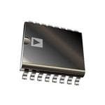
| 供应商器件封装 | 16-SOIC W |
| 分流电流—最大值 | 10 mA |
| 初始准确度 | +/- 1 mV |
| 包装 | 管件 |
| 参考类型 | Series Precision References |
| 商标 | Analog Devices |
| 安装类型 | 表面贴装 |
| 安装风格 | SMD/SMT |
| 容差 | ±5mV |
| 封装 | Tube |
| 封装/外壳 | 16-SOIC(0.295",7.50mm 宽) |
| 封装/箱体 | SOIC-16 |
| 工作温度 | -25°C ~ 85°C |
| 工厂包装数量 | 47 |
| 平均温度系数—典型值 | 1.5 PPM / C |
| 最大工作温度 | + 125 C |
| 最小工作温度 | - 55 C |
| 标准包装 | 1 |
| 温度系数 | 3ppm/°C |
| 电压-输入 | 10.8 V ~ 36 V |
| 电压-输出 | ±5V, ±10V |
| 电流-输出 | 10mA |
| 电流-阴极 | - |
| 电流-静态 | 10mA |
| 电源电流 | 10 mA |
| 系列 | AD588 |
| 输入电压 | 10.8 V to 36 V |
| 输出电压 | 10 V |
| 通道数 | 2 |


- 商务部:美国ITC正式对集成电路等产品启动337调查
- 曝三星4nm工艺存在良率问题 高通将骁龙8 Gen1或转产台积电
- 太阳诱电将投资9.5亿元在常州建新厂生产MLCC 预计2023年完工
- 英特尔发布欧洲新工厂建设计划 深化IDM 2.0 战略
- 台积电先进制程称霸业界 有大客户加持明年业绩稳了
- 达到5530亿美元!SIA预计今年全球半导体销售额将创下新高
- 英特尔拟将自动驾驶子公司Mobileye上市 估值或超500亿美元
- 三星加码芯片和SET,合并消费电子和移动部门,撤换高东真等 CEO
- 三星电子宣布重大人事变动 还合并消费电子和移动部门
- 海关总署:前11个月进口集成电路产品价值2.52万亿元 增长14.8%


PDF Datasheet 数据手册内容提取
Multiple Output, High Precision, Dual-Tracking Reference Data Sheet AD588 FEATURES FUNCTIONAL BLOCK DIAGRAM Low drift: 1.5 ppm/°C NOISE A3 OUT REDUCTION VHIGH A3 IN SENSE Low initial error: 1 mV 7 6 4 3 Pin programmable output +10 V, +5 V, ±5 V tracking, −5 V, −10 V A3 1 A3 OUT Flexible output force and sense terminals RB FORCE High impedance ground sense A1 A4 OUT 16-lead SOIC package and 16-lead CERDIP 14 R1 R4 SENSE MIL-STD-883-compliant versions available A4 OUT GENERAL DESCRIPTION R2 R5 A4 15 FORCE The AD588 represents a major advance in state-of-the-art R3 R6 2 +VS monolithic voltage references. Low initial error and low A2 AD588 temperature drift give the AD588 absolute accuracy performance 16 –VS previously not available in monolithic form. The AD588 uses a 5 9 10 8 12 11 13 dprroifpt rtireitmarmy iinogn -oifm hpiglahn stteadb, ibliutyr itehdi nZ feinlmer rdeisoisdteo rasn tdo l pasreorv-iwdea fer GAADIJN SGE+NNINSDE SGE–NNINSDE VLOW BAADLJ VCT A4 IN 00531-001 outstanding performance. Figure 1. The AD588 includes the basic reference cell and three additional PRODUCT HIGHLIGHTS amplifiers that provide pin programmable output ranges. The 1. The AD588 offers 12-bit absolute accuracy without any amplifiers are laser trimmed for low offset and low drift to maintain user adjustments. Optional fine-trim connections are the accuracy of the reference. The amplifiers are configured to provided for applications requiring higher precision. The allow Kelvin connections to the load and/or boosters for driving fine trimming does not alter the operating conditions of long lines or high current loads, delivering the full accuracy of the Zener or the buffer amplifiers, and so does not increase the AD588 where it is required in the application circuit. the temperature drift. The low initial error allows the AD588 to be used as a system 2. Output noise of the AD588 is very low, typically 6 µV p-p. reference in precision measurement applications requiring A pin is provided for additional noise filtering using an 12-bit absolute accuracy. In such systems, the AD588 can provide a external capacitor. known voltage for system calibration in software. The low drift 3. A precision ±5 V tracking mode with Kelvin output also allows compensation for the drift of other components in a connections is available with no external components. system. Manual system calibration and the cost of periodic Tracking error is less than 1 mV, and a fine trim is available recalibration can, therefore, be eliminated. Furthermore, the for applications requiring exact symmetry between the mechanical instability of a trimming potentiometer and the +5 V and −5 V outputs. potential for improper calibration can be eliminated by using 4. Pin strapping capability allows configuration of a wide the AD588 in conjunction with auto calibration software. variety of outputs: ±5 V, +5 V, +10 V, −5 V, and −10 V dual outputs or +5 V, −5 V, +10 V, and −10 V single outputs. The AD588 is available in seven versions. The AD588JQ and AD588KQ are packaged in a 16-lead CERDIP and are specified for 0°C to +70°C operation. The AD588AQ and AD588BQ are packaged in a 16-lead CERDIP, and the AD588ARWZ is packaged in a 16-lead SOIC, and they are specified for the −25°C to +85°C industrial temperature range. The ceramic AD588TE and AD588TQ grades are specified for the full military/aerospace temperature range. Rev. M Document Feedback Information furnished by Analog Devices is believed to be accurate and reliable. However, no responsibility is assumed by Analog Devices for its use, nor for any infringements of patents or other One Technology Way, P.O. Box 9106, Norwood, MA 02062-9106, U.S.A. rights of third parties that may result from its use. Specifications subject to change without notice. No license is granted by implication or otherwise under any patent or patent rights of Analog Devices. Tel: 781.329.4700 ©1986–2015 Analog Devices, Inc. All rights reserved. Trademarks and registered trademarks are the property of their respective owners. Technical Support www.analog.com
AD588 Data Sheet TABLE OF CONTENTS Features .............................................................................................. 1 Temperature Performance......................................................... 10 General Description ......................................................................... 1 Kelvin Connections .................................................................... 11 Functional Block Diagram .............................................................. 1 Dynamic Performance ............................................................... 13 Product Highlights ........................................................................... 1 Using the AD588 with Converters ............................................... 15 Revision History ............................................................................... 2 AD7535 14-Bit Digital-to-Analog Converter ......................... 15 Specifications ..................................................................................... 3 AD569 16-Bit Digital-to-Analog Converter ........................... 15 Absolute Maximum Ratings ............................................................ 4 Substituting for Internal References ........................................ 16 ESD Caution .................................................................................. 4 AD574A 12-Bit Analog-to-Digital Converter ........................ 16 Pin Configuration and Function Descriptions ............................. 5 Resistance Temperature Detector (RTD) Excitation ............. 16 Theory of Operation ........................................................................ 6 Boosted Precision Current Source ........................................... 17 Applications Information ................................................................ 7 Bridge Driver Circuits ............................................................... 17 Calibration ..................................................................................... 7 Outline Dimensions ....................................................................... 19 Noise Performance and Reduction ............................................ 9 Ordering Guide .......................................................................... 19 Turn-On Time ............................................................................ 10 REVISION HISTORY 11/05—Rev. D to Rev. E 11/15—Rev. L to Rev. M Updated Format .................................................................. Universal Changes to Figure 13 ...................................................................... 11 Added SOIC Version .......................................................... Universal Changes to Pin 14 in Figures ............................................ Universal 10/10—Rev. K to Rev. L Changes to Pin 9 and Pin 10 in Figures ........................... Universal Changes to Amplifier A2 Plus and Minus Input Labels Changes to Specifications Section ................................................... 3 in Figures ........................................................................ Throughout Added Table 3 .................................................................................... 4 Added Pin Configuration and Function Descriptions Section ... 5 9/10—Rev. J to Rev. K Added Table 4 .................................................................................... 5 Changes to Product Title ................................................................. 1 Changes to Grade in Reference and in Figure 12 ....................... 11 Updated Outline Dimensions ....................................................... 19 4/10—Rev. I to Rev. J Changes to Ordering Guide .......................................................... 19 Changes to Calibration Section ...................................................... 8 2/03—Rev. C to Rev. D 11/09—Rev. H to Rev. I Added KQ Model and Deleted SQ and TQ Models ...... Universal Changes to Figure 40 and Figure 41 ............................................. 18 Changes to General Description ..................................................... 1 Change to Product Highlights ......................................................... 1 10/09—Rev. G to Rev. H Changes to Specifications ................................................................. 2 Changes to General Description Section ...................................... 1 Changes to Ordering Guide ............................................................. 3 Updated Outline Dimensions ....................................................... 15 6/06—Rev. F to Rev. G Changes to Table 5 ............................................................................ 7 10/02—Rev. B to Rev. C Updated Outline Dimensions ....................................................... 19 Changes to General Description ..................................................... 1 Changes to Specifications ................................................................. 2 3/06—Rev. E to Rev. F Changes to Ordering Guide ............................................................. 3 Replaced Figure 5 ............................................................................. 8 Changes to Table 1 ............................................................................. 5 Updated Outline Dimensions ....................................................... 19 Deleted Figure 10c ............................................................................. 7 Updated Outline Dimensions ....................................................... 15 Rev. M | Page 2 of 20
Data Sheet AD588 SPECIFICATIONS Typical at 25°C, 10 V output, V = ±15 V, unless otherwise noted. S Specifications shown in boldface are tested on all production units at final electrical test. Results from those tests are used to calculate outgoing quality levels. All minimum and maximum specifications are guaranteed, although only those shown in boldface are tested on all production units. Table 1. AD588JQ/AD588AQ AD588BQ/AD588KQ AD588ARWZ Parameter1 Min Typ Max Min Typ Max Min Typ Max Unit OUTPUT VOLTAGE ERROR +10 V, −10 V Outputs ±3 −1 +1 −5 +5 mV +5 V, −5 V Outputs ±3 −1 +1 −5 +5 mV ±5 V TRACKING MODE Symmetry Error ±1.5 ±0.75 ±1.5 mV OUTPUT VOLTAGE DRIFT 0°C to 70°C (J, K, B) ±2 ±3 ±1.5 ±2 ±3 ppm/°C −25°C to +85°C (A, B) ±3 ±3 ±3 ppm/°C GAIN ADJ AND BAL ADJ2 Trim Range ±4 ±4 ±4 mV Input Resistance 150 150 150 kΩ LINE REGULATION TMIN to TMAX3 ±200 ±200 ±200 µV/V LOAD REGULATION TMIN to TMAX +10 V Output, 0 mA < IOUT < 10 mA ±50 ±50 ±50 µV/mA −10 V Output, −10 mA < IOUT < 0 mA ±50 ±50 ±50 µV/mA SUPPLY CURRENT TMIN to TMAX 6 10 6 10 6 10 mA Power Dissipation 180 300 180 300 180 300 mW OUTPUT NOISE (Any Output) 0.1 Hz to 10 Hz 6 6 6 µV p-p Spectral Density, 100 Hz 100 100 100 nV/√Hz LONG-TERM STABILITY (at 25°C) 15 15 15 ppm/1000 hr BUFFER AMPLIFIERS Offset Voltage 100 10 100 µV Offset Voltage Drift 1 1 1 µV/°C Bias Current 20 20 20 nA Open-Loop Gain 110 110 110 dB Output Current (A3, A4) −10 +10 −10 +10 −10 +10 mA Common-Mode Rejection (A3, A4) V = 1 V p-p 100 100 100 dB CM Short Circuit Current 50 50 50 mA TEMPERATURE RANGE Specified Performance J, K Grades 0 70 0 70 °C A, B Grades −25 +85 −25 +85 −25 +85 °C 1Specifications tested using ±5 V configuration, unless otherwise indicated. See Figure 4 through Figure 6 for output configurations at +10 V, −10 V, +5 V, −5 V and ±5 V. 2Gain and balance adjustments guaranteed capable of trimming output voltage error and symmetry error to zero. 3For ±10 V output, ±VS can be as low as ±12 V. See Table 3 for test conditions at various voltages. Rev. M | Page 3 of 20
AD588 Data Sheet ABSOLUTE MAXIMUM RATINGS Stresses at or above those listed under Absolute Maximum Table 2. Ratings may cause permanent damage to the product. This is a Parameter Rating stress rating only; functional operation of the product at these +V to −V 36 V S S or any other conditions above those indicated in the operational Power Dissipation (25°C) 600 mW section of this specification is not implied. Operation beyond Storage Temperature Range −65°C to +150°C the maximum operating conditions for extended periods may Lead Temperature (Soldering 10 sec) 300°C affect product reliability. Package Thermal Resistance (θ /θ ) 90°C/25°C/W JA JC Output Protection All outputs safe if shorted to ground ESD CAUTION Table 3. Test Conditions Voltage Conditions +10 V Output −V = −15 V, +13.5 V ≤ +V ≤ +18 V S S −10 V Output −18 V ≤ −VS ≤ −13.5 V, +VS = +15 V ±5 V Output +V = +18 V, −V = −18 V S S +V = +10.8 V, −V = −10.8 V S S Rev. M | Page 4 of 20
Data Sheet AD588 PIN CONFIGURATION AND FUNCTION DESCRIPTIONS A3 OUT FORCE 1 16 –VS +VS 2 15 A4 OUT FORCE A3 OUT SENSE 3 14 A4 OUT SENSE A3 IN 4 AD588 13 A4 IN TOP VIEW GAINADJ 5 (Not to Scale)12 BALADJ VHIGH 6 11 VCT NOISE 7 10 GND SENSE –IN REDUCVTLIOOWN 8 9 GND SENSE +IN 00531-002 Figure 2. Pin Configuration Table 4. Pin Function Descriptions Pin No. Mnemonic Description 1 A3 OUT FORCE Output from Buffering Amplifier 3 with Kelvin Force. Connect to Pin 3. 2 +V Positive Power Supply. S 3 A3 OUT SENSE Output from Buffering Amplifier 3 with Kelvin Sense. Connect to Pin 1. 4 A3 IN Positive Input to Amplifier 3. Connect to V , Pin 6. HIGH 5 GAIN ADJ Reference Gain Adjustment for Calibration. See the Calibration section. 6 V Unbuffered Reference High Output. HIGH 7 NOISE REDUCTION Noise Filtering Pin. Connect external 1 µF capacitor to ground to reduce the output noise (see the Noise Performance and Reduction section). Can be left open. 8 V Unbuffered Reference Low Output. LOW 9 GND SENSE +IN Positive Input to the Ground Sense Amplifier. 10 GND SENSE −IN Negative Input to the Ground Sense Amplifier. 11 V Center Tap Voltage used for Calibration. See the Calibration section. CT 12 BAL ADJ Reference Centering Adjustment for Calibration. See the Calibration section. 13 A4 IN Positive Input to Amplifier 4. Connect to V , Pin 8. LOW 14 A4 OUT SENSE Output of Buffering Amplifier 4 with Kelvin Sense. Connect to Pin 15. 15 A4 OUT FORCE Output of Buffering Amplifier 4 with Kelvin Force. Connect to Pin 14. 16 −V Negative Power Supply. S Rev. M | Page 5 of 20
AD588 Data Sheet THEORY OF OPERATION The AD588 consists of a buried Zener diode reference, Ground sensing for the circuit is provided by Amplifier A2. The amplifiers used to provide pin programmable output ranges, noninverting input (Pin 9) senses the system ground, which is and associated thin-film resistors, as shown in Figure 3. The transferred to the point on the circuit where the inverting input temperature compensation circuitry provides the device with a (Pin 10) is connected. This can be Pin 6, Pin 8, or Pin 11. The temperature coefficient of 1.5 ppm/°C or less. output of A2 drives Pin 8 to the appropriate voltage. Thus, if Pin 10 is connected to Pin 8, the V pin is the same voltage as LOW Amplifier A1 performs several functions. A1 primarily acts to the system ground. Alternatively, if Pin 10 is connected to the amplify the Zener voltage from 6.5 V to the required 10 V output. V pin, it is a ground; and Pin 6 and Pin 8 are +5 V and −5 V, CT In addition, A1 provides for external adjustment of the 10 V output respectively. through Pin 5, GAIN ADJ. Using the bias compensation resistor between the Zener output and the noninverting input to A1, a Amplifier A3 and Amplifier A4 are internally compensated and capacitor can be added at the NOISE REDUCTION pin (Pin 7) are used to buffer the voltages at Pin 6, Pin 8, and Pin 11, as well to form a low-pass filter and reduce the noise contribution of the as to provide a full Kelvin output. Thus, the AD588 has a full Zener to the circuit. Two matched 10 kΩ nominal thin-film Kelvin capability by providing the means to sense a system resistors (R4 and R5) divide the 10 V output in half. Pin V ground and provide forced and sensed outputs referenced to CT (Pin 11) provides access to the center of the voltage span and that ground. BAL ADJ (Pin 12) can be used for fine adjustment of this Note that both positive and negative supplies are required for division. operation of the AD588. NOISE A3 OUT REDUCTION VHIGH A3 IN SENSE 7 6 4 3 A3 1 A3 OUT RB FORCE A1 A4 OUT 14 R1 R4 SENSE A4 OUT R2 R5 A4 15 FORCE R3 R6 2 +VS A2 AD588 16 –VS 5 9 10 8 12 11 13 GAADIJN SGE+NNINSDE SGE–NNINSDE VLOW BAADLJ VCT A4 IN 00531-003 Figure 3. AD588 Functional Block Diagram Rev. M | Page 6 of 20
Data Sheet AD588 APPLICATIONS INFORMATION The AD588 can be configured to provide +10 V and –10 V Amplifier A3 and Amplifier A4 can be used interchangeably. reference outputs, as shown in Figure 4 and Figure 6, respectively. However, the AD588 is tested (and the specifications are It can also be used to provide +5 V, −5 V, or a 5 V tracking guaranteed) with the amplifiers connected, as indicated in reference, as shown in Figure 5. Table 5 details the appropriate Figure 4 and Table 5. When either A3 or A4 is unused, its pin connections for each output range. In each case, Pin 9 is output force and sense pins should be connected or the input connected to system ground, and power is applied to Pin 2 tied to ground. and Pin 16. Two outputs of the same voltage can be obtained by connecting The architecture of the AD588 provides ground sense and both A3 and A4 to the appropriate unbuffered output on Pin 6, uncommitted output buffer amplifiers that offer the user a great Pin 8, or Pin 11. Performance in these dual-output configurations deal of functional flexibility. The AD588 is specified and tested typically meets data sheet specifications. in the configurations shown in Figure 6. The user can choose to CALIBRATION take advantage of the many other configuration options available with the AD588. However, performance in these configurations Generally, the AD588 meets the requirements of a precision is not guaranteed to meet the extremely stringent data sheet system without additional adjustment. Initial output voltage specifications. error of 1 mV and output noise specs of 10 µV p-p allow for accuracies of 12 bits to 16 bits. However, in applications where As indicated in Table 5, a +5 V buffered output can be provided an even greater level of accuracy is required, additional calibra- using Amplifier A4 in the +10 V configuration (Figure 4). A tion may be called for. Provision for trimming has been made −5 V buffered output can be provided using Amplifier A3 in the through the use of the GAIN ADJ and BAL ADJ pins (Pin 5 and −10 V configuration (Figure 6). Specifications are not guaranteed Pin 12, respectively). for the +5 V or −5 V outputs in these configurations. Performance is similar to that specified for the +10 V or −10 V outputs. The AD588 provides a precision 10 V span with a center tap (V ) that is used with the buffer and ground sense amplifiers to CT As indicated in Table 5, unbuffered outputs are available at achieve the voltage output configurations in Table 5. GAIN ADJ Pin 6, Pin 8, and Pin 11. Loading of these unbuffered outputs and BAL ADJ can be used in any of these configurations to trim impairs circuit performance. the magnitude of the span voltage and the position of the center tap within the span. The gain adjust should be performed first. Although the trims are not interactive within the device, the gain trim moves the balance trim point as it changes the magnitude of the span. Table 5. Pin Connections Connect Unbuffered1 Output on Pins Buffered Output Buffered Output on Pins Range Pin 10 to Pin −10 V −5 V 0 V +5 V +10 V Connections −10 V −5 V 0 V +5 V +10 V +10 V 8 8 11 6 11 to 13, 14 to 15, 15 6 to 4, and 3 to 1 1 −5 V or +5 V 11 8 11 6 8 to 13, 14 to 15, 15 6 to 4, and 3 to 1 1 −10 V 6 8 11 6 8 to 13, 14 to 15, 15 11 to 4, and 3 to 1 1 +5 V 11 6 6 to 4 and 3 to 1 1 −5 V 11 8 8 to 13 and 14 to 15 15 1 Unbuffered outputs should not be loaded. Rev. M | Page 7 of 20
AD588 Data Sheet Figure 5 shows gain and balance trims in a +5 V and −5 V 39kΩ +15V tracking configuration. A 100 kΩ, 20-turn potentiometer NOISE 1µF REDUCTION is used for each trim. The potentiometer for gain trim is connected between Pin 6 (V ) and Pin 8 (V ) with the HIGH LOW wiper connected to Pin 5 (GAIN ADJ). The potentiometer is A3 +5V adjusted to produce exactly 10 V between Pin 1 and Pin 15, the RB amplifier outputs. The balance potentiometer, also connected A1 AD588 between Pin 6 and Pin 8 with the wiper to Pin 12 (BAL ADJ), is R1 R4 then adjusted to center the span from +5 V to −5 V. R2 A4 –5V R5 Trimming in other configurations works in exactly the same +VS +15V manner. When producing +10 V and +5 V, GAIN ADJ is used R3 R6 0.1µF to trim +10 V and BAL ADJ is used to trim +5 V. In the −10 V A2 SYSTEM –VS GROUND and −5 V configuration, GAIN ADJ is again used to trim the 0.1µF magnitude of the span, −10 V, while BAL ADJ is used to trim –15V the center tap, −5 V. SYSTEM GROUND Trimming the AD588 introduces no additional errors over 100kΩ temperature, so precision potentiometers are not required. For 20T BALANCE single-output voltage ranges, or in cases when balance adjust is ADJUST nadojtu rsetq ius inreodt ,r ePqinu i1r2ed s,h Poiunl d5 bshe ocuolndn beec tleedft tfolo Paitnin 1g1. . If gain GAIN10 2A00DkTΩJUST 00531-005 Figure 5. +5 V and −5 V Outputs In single output configurations, GAIN ADJ is used to trim outputs utilizing the full span (+10 V or −10 V), while BAL ADJ is used to trim outputs using half the span (+5 V or −5 V). 0.1µF Input impedance on both the GAIN ADJ and BAL ADJ pins is NOISE approximately 150 kΩ. The GAIN ADJ trim network effectively 0.1µF REDUCTION 7 6 4 3 attenuates the 10 V across the trim potentiometer by a factor of about 1500 to provide a trim range of −3.5 mV to +7.5 mV with a resolution of approximately 550 μV/turn (20-turn potentiome- RB A3 1 –5V ter). The BAL ADJ trim network attenuates the trim voltage by A1 AD588 a factor of about 1400, providing a trim range of ±4.5 mV with 14 R1 R4 resolution of 450 μV/turn. R2 A4 15 –10V R5 7 6 4 3 +VS 2 +15V R3 R6 0.1µF A3 1 +10V A2 SYSTEM RB –VS 16 GROUND 0.1µF A1 5 9 10 8 12 11 13 –15V 14 R1 R4 SYSTEM R2 R5 A4 15 +5V GROUND 00531-006 +VS 2 +15V Figure 6. −10 V Output R3 R6 AD588 0.1µF A2 SYSTEM –VS 16 GROUND 0.1µF 5 9 10 8 12 11 13 –15V GSRYOSTUENMD 00531-004 Figure 4. +10 V Output Rev. M | Page 8 of 20
Data Sheet AD588 NOISE PERFORMANCE AND REDUCTION The noise generated by the AD588 is typically less than 6 µV p-p over the 0.1 Hz to 10 Hz band. Noise in a 1 MHz bandwidth is approximately 600 µV p-p. The dominant source of this noise is the buried Zener, which contributes approximately 100 nV/√Hz. In 1µV comparison, the op amp’s contribution is negligible. Figure 7 shows the 0.1 Hz to 10 Hz noise of a typical AD588. If further noise reduction is desired, an optional capacitor, C , N can be added between the NOISE REDUCTION pin and gTrhoius nfodr, mass sah loowwn-p inas Fs ifgiluterer 5w.i th the 4 kΩ R on the output of 00531-007 B Figure 7. 0.1 Hz to 10 Hz Noise (0.1 Hz to 10 Hz BPF the Zener cell. A 1 µF capacitor has a 3 dB point at 40 Hz and with Gain of 1000 Applied) reduces the high frequency noise (to 1 MHz) to about 200 µV p-p. Figure 8 shows the 1 MHz noise of a typical AD588 both with and without a 1 µF capacitor. Note that a second capacitor is needed in order to implement CN = 1mF the noise reduction feature when using the AD588 in the −10 V mode (Figure 6). The noise reduction capacitor is limited to 0.1 µF maximum in this mode. NO CN 00531-008 Figure 8. Effect of 1 µF Noise Reduction Capacitor on Broadband Noise Rev. M | Page 9 of 20
AD588 Data Sheet TURN-ON TIME Output turn-on time is modified when an external noise reduction capacitor is used. When present, this capacitor Upon application of power (cold start), the time required for presents an additional load to the internal Zener diode current the output voltage to reach its final value within a specified source, resulting in a somewhat longer turn-on time. In the case error band is the turn-on settling time. Two components of a 1 µF capacitor, the initial turn-on time is approximately normally associated with this are the time for active circuits to 60 ms (see Figure 11). settle and the time for thermal gradients on the chip to stabilize. Note that if the noise reduction feature is used in the ±5 V Figure 9 and Figure 10 show the turn-on characteristics of the configuration, a 39 kΩ resistor between Pin 6 and Pin 2 is AD588. The settling is about 600 µs. Note the absence of any required for proper startup. thermal tails when the horizontal scale is expanded to 2 ms/cm in Figure 10. +VS +VS –VS VOUT VOUT 00531-009 Figure 11. Turn-On with CN = 1 µF 00531-011 Figure 9. Electrical Turn-On TEMPERATURE PERFORMANCE The AD588 is designed for precision reference applications where temperature performance is critical. Extensive temperature testing +VS ensures that the device’s high level of performance is maintained over the operating temperature range. Figure 12 shows typical output temperature drift for the AD588BQ and illustrates the test methodology. The box in Figure 12 is VOUT bounded on the sides by the operating temperature extremes and on top and bottom by the maximum and minimum output voltages measured over the operating temperature range. The slope of the diagonal drawn from the lower left corner of the 00531-010 box determines the performance grade of the device. Figure 10. Extended Time Scale Turn-On VMAX– VMIN SLOPE =T.C. = (TMAX – TMIN) × 10 × 1–4 10.0013V – 10.00025V (85°C – –25°C) × 10 × 10–4 10.002 = 0.95ppm/°C s) Volt VMAX UT (10.001 P T U O VMIN 10.000 –3V5MI–N1T5EM5PER2A5TUR4E5 (°C65)VM8A5X 00531-012 Figure 12. Typical AD588BQ Temperature Drift Rev. M | Page 10 of 20
Data Sheet AD588 Each AD588 A and B grade unit is tested at −25°C, 0°C, +25°C, The AD588 has three amplifiers that can be used to implement +50°C, +70°C, and +85°C. This approach ensures that the Kelvin connections. Amplifier A2 is dedicated to the ground variations of output voltage that occur as the temperature force-sense function, while uncommitted Amplifier A3 and changes within the specified range is contained within a box Amplifier A4 are free for other force-sense chores. whose diagonal has a slope equal to the maximum specified R drift. The position of the box on the vertical scale changes from device to device as initial error and the shape of the curve vary. I = 0 V = 10V Maximum height of the box for the appropriate temperature R V = 10V – RIL R raa cnogme bisi nshatoiownn oinf hFiigghu raec c1u3r. aDcyu palnicda stitoabnl eo ft ethmespee rreastuulrtes creoqnutirroels 10V–+ IL RLOAD I = 0 V = 10V – RIILL RLOAD 00531-014 in a test system. Evaluation of the AD588 produces a curve Figure 14. Advantage of Kelvin Connection similar to that in Figure 12, but output readings may vary, depending on the test methods and equipment utilized. In some single-output applications, one amplifier can be unused. In such cases, the unused amplifier should be DEVICE MAXIMUM OUTPUT CHANGE (mV) GRADE 0°CTO +70°C –25°CTO +85°C connected as a unity-gain follower (force and sense pin tied AD588J 2.10 together), and the input should be connected to ground. AD588K 1.05 AADD558888BA 1.401 .(0T5YP) 33..3300 00531-013 Afunn cutniounses,d a asm wpellilf. iFeirg suercet i1o5n t charno ubgeh u Fseigdu froer 1 o9t hshero wci rtchuei tt ypical Figure 13. Maximum Output Change—mV performance of A3 and A4. KELVIN CONNECTIONS 100 0 Force and sense connections, also referred to as Kelvin 80 –30 connections, offer a convenient method of eliminating the GAIN Tet(hVfhfeeEe Rcl KoRtOsaeR dlo v= fic n vuR ocr ×lroten aIngnL)tee a acdtnt ritdooh npew soli orifn aeFd ric.ge i urscirsuet ai1tn 4wc oeir vpeesrr.oc Aodmus cseees e atnnh e ien pr rFrooirgb u lerme 1 b4y, N-LOOP GAIN (dB)6400 PHASE ––6900 HASE (Degrees) including the wire resistance within the forcing loop of the OPE20 –120 P amplifier and sensing the load voltage. The amplifier corrects 0 –150 for any errors in the load voltage. In the circuit shown, the output of the amplifier would actually be at 10 V + V , and the voltage at the load would be the desired 10 V. ERROR –2010 100 1kFREQU1E0NkCY (Hz1)00k 1M 10M–180 00531-015 Figure 15. Open-Loop Frequency Response (A3, A4) Rev. M | Page 11 of 20
AD588 Data Sheet 110 110 VS = ±15V WITH VS = ±15V 1V p-p SINEWAVE VCM = 1V p-p +25°C B)100 100 N (d +SUPPLY O TI 80 80 C JE B) E d LY R 60 RR (60 P –SUPPLY M P C U R S 40 40 E W O P 20 20 1010 100 1kFREQU1E0NkCY (Hz1)00k 1M 10M 00531-016 010 100 1kFREQU1E0NkCY (Hz1)00k 1M 10M 00531-019 Figure 16. Power Supply Rejection vs. Frequency (A3, A4) Figure 19. Common-Mode Rejection vs. Frequency (A3, A4) 100 90 Hz) √80 V/ n Y (70 T NSI60 E D L 50 A R T40 C E SP30 E S OI20 00531-017 N1001 10 FREQU1E0N0CY (Hz) 1k 10k 00531-020 Figure 20. Input Noise Voltage Spectral Density Figure 17. Unity-Gain Follower Pulse Response (Large Signal) 00531-018 Figure 18. Unity-Gain Follower Pulse Response (Small Signal) Rev. M | Page 12 of 20
Data Sheet AD588 DYNAMIC PERFORMANCE In some applications, a varying load can be both resistive and capacitive in nature or can be connected to the AD588 by a long The output buffer amplifiers (A3 and A4) are designed to capacitive cable. Figure 25 and Figure 26 display the output provide the AD588 with static and dynamic load regulation amplifier characteristics driving a 1000 pF, 0 mA to 10 mA load. superior to less complete references. Many analog-to-digital and digital-to-analog converters present transient current loads to A3 ORA4 the reference, and poor reference response can degrade converter pofe rtfhoer mAaDn5c8e.8 F oiguutprue t2 a1m apnldif Fieirg udrreiv 2in2 gd ais 0p lmayA th teo c1h0a mraAct eloriasdti.c s 1000pCFL 1kΩ VOUT A3 ORA4 10V VL 100VV 00531-025 Figure 25. Capacitive Load Transient Response Test Circuit VOUT IL 1kΩ 10V VL 100VV 00531-021 Figure 21. Transient Load Test Circuit CL = 0 CL = 1000pF VOUT VL 00531-026 Figure 26. Output Response with Capacitive Load VL Figure 27 and Figure 28 display the crosstalk between output 00531-022 aamndp olifffiseerts .b Tyh 1e0 t Vop, w trhaiclee tshheo wous ttphuet oouf tApu3t i so fs uAb4j,e cdtce-dc otou pal e0d m A Figure 22. Large-Scale Transient Response to 10 mA load current step. The transient at A4 settles in about Figure 23 and Figure 24 display the output amplifier 1 μs, and the load-induced offset is about 100 μV. characteristics driving a 5 mA to 10 mA load, a common situation found when the reference is shared among multiple converters or is used to provide a bipolar offset current. A4 VOUT A3 + 1kΩ + A3 ORA4 VOUT –10V VL 100VV 10V– 00531-027 + IL 2kΩ 2kΩ Figure 27. Load Crosstalk Test Circuit 10V– VL 100VV 00531-023 Figure 23. Transient and Constant Load Test Circuit VOUT 1mV/CM VOUT VOUT 200mV/CM VL 00531-028 Figure 28. Load Crosstalk VL 00531-024 Figure 24. Transient Response 5 mA to10 mA Load Rev. M | Page 13 of 20
AD588 Data Sheet Attempts to drive a large capacitive load (in excess of 1000 pF) can result in ringing or oscillation, as shown in the step response photo (Figure 29). This is due to the additional pole formed by the load capacitance and the output impedance of the amplifier, VIN which consumes phase margin. The recommended method of driving capacitive loads of this magnitude is shown in Figure 30. The 150 Ω resistor isolates the capacitive load from the output stage, while the 10 kΩ resistor provides a dc feedback path and preserves the output accuracy. VOUT The 1 µF capacitor provides a high frequency feedback loop. The performance of this circuit is shown in Figure 31. 00531-031 Figure 31. Output Amplifier Step Response Using Figure 30 Compensation VIN VOUT 00531-029 Figure 29. Output Amplifier Step Response, CL = 1 µF 10kΩ 1µF 150Ω VOUT + CL 1µF –VIN 00531-030 Figure 30. Compensation for Capacitive Loads Rev. M | Page 14 of 20
Data Sheet AD588 USING THE AD588 WITH CONVERTERS The AD588 is an ideal reference for a wide variety of analog-to- AD569 16-BIT DIGITAL-TO-ANALOG CONVERTER digital and digital-to-analog converters. Several representative Another application that fully utilizes the capabilities of the AD588 examples follow. is supplying a reference for the AD569, as shown in Figure 33. AD7535 14-BIT DIGITAL-TO-ANALOG CONVERTER Amplifier A2 senses system common and forces VCT to assume this value, producing +5 V and −5 V at Pin 6 and Pin 8, respectively. High resolution CMOS digital-to-analog converters require a Amplifier A3 and Amplifier A4 buffer these voltages out to the reference voltage of high precision to maintain rated accuracy. appropriate reference force-sense pins of the AD569. The full The combination of the AD588 and AD7535 takes advantage of Kelvin scheme eliminates the effect of the circuit traces or wires and the initial accuracy, drift, and full Kelvin output capability of the the wire bonds of the AD588 and AD569 themselves, which would AD588, as well as the resolution, monotonicity, and accuracy of the otherwise degrade system performance. AD7535 to produce a subsystem with outstanding characteristics (see Figure 32). N.C. VDD 28 26 VREFS 1 3 RFS 7 6 4 3 14-BIT DAC 4 IOUT +10V VREF A3 1 2 RB 14 AD7535 A1 AD588 AGNDS 14 5 R1 R4 DAC REGISTER 23 LDAC AGNDF R2 A4 15 6 R5 MS LS 24 CSLSB INPUT INPUT R3 R6 2 +VS REGISTER REGISTER A2 22 CSMSB 16 –VS 25 WR 5 9 10 8 12 11 13 DB813 D2B10 DG7ND V2S7S 00531-032 Figure 32. AD588/AD7535 Connections +12V –12V +VS –VS 2 16 6 4 1 28 VH A3 + IN A3 +VREF OUT FORCE A3 1 3 A3 – IN +5V +SVERNESFE AD569 3 2 A1 10kΩ 12 S S S E E VCT E L L 11 GE T E VOUT 10kΩ A2 – IN10 MECT APCT 17 –+55VV TO A2 A2 + IN 9 NTOR OR –VREF A4 – IN –5V SENSE 14 16 AD588 A4 –VREF OUT FORCE A4 15 15 VL A4 + IN 8 13 8 MSBs 8 LSBs GND 18 LATCHES 13 14 12 9 7 4 19 22 24 27 8 23 CS LDACDB15 DB0HBE LBE 00531-033 Figure 33. High Accuracy ±5 V Tracking Reference for AD569 Rev. M | Page 15 of 20
AD588 Data Sheet SUBSTITUTING FOR INTERNAL REFERENCES RESISTANCE TEMPERATURE DETECTOR (RTD) EXCITATION Many converters include built-in references. Unfortunately, such references are the major source of drift in these converters. The RTD is a circuit element whose resistance is characterized By using a more stable external reference like the AD588, drift by a positive temperature coefficient. A measurement of performance can be improved dramatically. resistance indicates the measured temperature. Unfortunately, the resistance of the wires leading to the RTD often adds error to this AD574A 12-BIT ANALOG-TO-DIGITAL CONVERTER measurement. The 4-wire ohms measurement overcomes this The AD574A is specified for gain drift from 10 ppm/°C to problem. This method uses two wires to bring an excitation 50 ppm/°C (depending on grade), using its on-chip reference. current to the RTD and two additional wires to tap off the resulting The reference contributes typically 75% of this drift. Using an RTD voltage. If these additional two wires go to a high input AD588 as a reference source can improve the total drift by a impedance measurement circuit, the effect of their resistance is factor of 3 to 4. negligible. They therefore transmit the true RTD voltage. Using this combination can result in apparent increases in I = 0 R full-scale error due to the difference between the on-board R + reference, by which the device is laser-trimmed, and the external reference, with which the device is actually applied. IEXC RTD VOUT α RRTD – Tthhee e oxnte-rbnoaalr rde freerfeenrecnec ies issp sepceifciiefdie tdo tboe b 1e0 1 V0 V± 1± m10V0. mThVi,s w mhaiyle R I =R 0 00531-034 result in up to 101 mV of apparent full-scale error beyond the Figure 34. 4-Wire Ohms Measurement ±25 mV specified AD574A gain error. External Resistor R2 and Resistor R3 allow this error to be nulled. Their contribution to full-scale drift is negligible. The high output drive capability allows the AD588 to drive up to six converters in a multiconverter system. All converters have gain errors that track to better than ±5 ppm/°C. 2 12√8 STS 28 3 CS HIGH 27 BITS 24 4 AO 5 R/C MIDDLE 23 7 6 4 3 BITS R1 6 CE AD574A 20 50Ω A3 1 10 REF IN 19 RB 50R03Ω 8 REF OUT LBOITWS 16 A1 AD588 20 TURN 14 R1 R4 R2 12 BIPP OFF +5V 1 61.9Ω R2 R5 A4 15 VIN 13 10VIN +15V 7 10V 14 20VIN –15V 11 R3 R6 2 +VS 9 ANA COM DIG 15 COM A2 16 –VS 5 9 10 8 12 11 13 00531-035 Figure 35. AD588/AD574A Connections Rev. M | Page 16 of 20
Data Sheet AD588 A practical consideration when using the 4-wire ohms technique with an RTD is the self-heating effect that the excitation current 7 6 4 3 RVICSHAY S102C has on the temperature of the RTD. The designer must choose OR SIMILAR the smallest practical excitation current that still gives the desired A3 1 RB resolution. RTD manufacturers usually specify the self-heating A1 AD588 effect of each of their models or types of RTDs. R1 R4 14 RC = 10kΩ 1.0mA Figure 36 shows an AD588 providing the precision excitation 0.01% R2 A4 15 + current for a 100 Ω RTD. The small excitation current of 1 mA R5 dissipates a mere 0.1 mW of power in the RTD. 100Ω VOUT R3 R6 2 +VS – BOOSTED PRECISION CURRENT SOURCE A2 16 –VS –15V In the RTD current-source application, the load current is limited OR GROUND 5 9 10 8 12 11 13 to ±10 mA by the output drive capability of Amplifier A3. In the event that more drive current is needed, a series-pass transistor ccaunrr bene ti.n Asecrctuerda cinys aidned tdhrei ffte epdebrfaocrkm loanocpe t oar pe ruonvaidffee chtiegdh ebry the R0.T2D4° C= /Ωm KW4 S51E5LF-HEATING 00531-036 pass transistor. Figure 36. Precision Current Source for RTD BRIDGE DRIVER CIRCUITS 7 6 4 3 VCC The Wheatstone bridge is a common transducer. In its simplest 220Ω form, a bridge consists of four two-terminal elements connected A3 1 Q1 to form a quadrilateral, a source of excitation connected along RB A1 AD588 one of the diagonals and a detector comprising the other diagonal. 14 R1 R4 Figure 38 shows a simple bridge driven from a unipolar excitation R2 A4 15 supply. EO, a differential voltage, is proportional to the deviation R5 of the element from the initial bridge values. Unfortunately, this 10V bridge output voltage is riding on a common-mode voltage R3 R6 2 +VS IL =RC equal to approximately V /2. Further processing of this signal A2 IN 16 –VS may necessarily be limited to high common-mode rejection 5 9 10 8 12 11 13 techniques, such as instrumentation or isolation amplifiers. LIMITED BY Q1 AND RC POWER Figure 39 shows the same bridge transducer, this time driven DISSIPATION ferloimmi naa pteasi rt hoef bcoipmolmaro snu-pmpolidees. vTohltiasg ceo annfidg urerlaatxioens tihdee ally LOAD 00531-037 Figure 37. Boosted Precision Current Source restrictions on any processing elements that follow. R4 R3 + – + VIN – EO R1 R2 00531-038 Figure 38. Bridge Transducer Excitation—Unipolar Drive + V1 R4 R3 – – + EO V2 +– R1 R2 00531-039 Figure 39. Bridge Transducer Excitation—Bipolar Drive Rev. M | Page 17 of 20
AD588 Data Sheet As shown in Figure 40, the AD588 is an excellent choice for the +15V control element in a bipolar bridge driver scheme. Transistor Q1 220Ω Q1 = and Transistor Q2 serve as series-pass elements to boost the 2N3904 current drive capability to the 28 mA required by a typical 7 6 4 3 350 Ω bridge. A differential gain stage can still be required if the bridge balance is not perfect. Such gain stages can be expensive. A3 1 Additional common-mode voltage reduction is realized by RB –EO+ A1 AD588 using the circuit illustrated in Figure 41. A1, the ground sense 14 amplifier, serves the supplies on the bridge to maintain a virtual R1 R4 gceronutenrd t aatp o ins en coewn tseirn tgalpe.- Tenhde evdo l(traegfee rthenatc eapdp teoa grsr oounn thde) aonpdpo csaitne R2 R5 A4 15 220Ω Q2N2 3=906 be amplified by a less expensive circuit. –15V R6 2 +VS R3 A2 16 –VS 5 9 10 8 12 11 13 00531-040 Figure 40. Bipolar Bridge Drive +15V 220Ω Q1 = 2N3904 7 6 4 3 A3 1 AD OP-07 RB + A1 AD588 VOUT 14 R1 – R1 R4 220Ω Q2 = R2 A4 15 2N3906 R5 R2 –15V R3 R6 2 +VS A2 16 –VS 5 9 10 8 12 11 13 00531-041 Figure 41. Floating Bipolar Bridge Drive with Minimum CMV Rev. M | Page 18 of 20
Data Sheet AD588 OUTLINE DIMENSIONS 10.50 (0.4134) 10.10 (0.3976) 16 9 7.60 (0.2992) 7.40 (0.2913) 1 8 10.65 (0.4193) 10.00 (0.3937) 1.27 (0.0500) 0.75 (0.0295) BSC 2.65 (0.1043) 0.25 (0.0098) 45° 0.30 (0.0118) 2.35 (0.0925) 8° 0.10 (0.0039) 0° COPLANARITY 0.10 0.51 (0.0201) SPLEAATNIENG 0.33 (0.0130) 1.27 (0.0500) 0.31 (0.0122) 0.20 (0.0079) 0.40 (0.0157) COMPLIANTTO JEDEC STANDARDS MS-013-AA C(RINEOFNPEATRRREOENNLCLTEIHN EOGSN EDLSIYM)AEANNRDSEI AORRNOESU NANORDEET DAIN-PO MPFRIFLO LMPIIMRLELIATIMTEEER TFSEO; RIRN ECUQHSU EDI VIINMA LEDENENSSTIIOGSN NFS.OR 032707-B Figure 42. 16-Lead Standard Small Outline Package [SOIC_W] Wide Body (RW-16) Dimensions shown in millimeters and (inches) 0.005 (0.13) MIN 0.098 (2.49) MAX 16 9 0.310 (7.87) 0.220 (5.59) 1 8 PIN 1 0.100 (2.54) BSC 0.320 (8.13) 0.290 (7.37) 0.840 (21.34) MAX 0.060 (1.52) 0.200 (5.08) 0.015 (0.38) MAX 0.150 0.200 (5.08) (3.81) 0.125 (3.18) MIN SEATING 0.015 (0.38) 0.023 (0.58) 0.070 (1.78) PLANE 15° 0.008 (0.20) 0.014 (0.36) 0.030 (0.76) 0° CONTROLLING DIMENSIONS ARE IN INCHES; MILLIMETER DIMENSIONS (IN PARENTHESES) ARE ROUNDED-OFF INCH EQUIVALENTS FOR REFERENCE ONLY AND ARE NOT APPROPRIATE FOR USE IN DESIGN. Figure 43. 16-Lead Ceramic Dual In-Line Package [CERDIP] (Q-16) Dimensions shown in inches and (millimeters) ORDERING GUIDE Temperature Temperature Package Model1, 2 Initial Error (mV) Coefficient3 Range (°C) Package Description Option AD588ARWZ 5 3 ppm/°C −25 to +85 16-Lead Standard Small Outline Package [SOIC-W] RW-16 AD588AQ 3 3 ppm/°C −25 to +85 16-Lead Ceramic Dual In-Line Package [CERDIP] Q-16 AD588BQ 1 1.5 ppm/°C −25 to +85 16-Lead Ceramic Dual In-Line Package [CERDIP] Q-16 AD588JQ 3 3 ppm/°C 0 to 70 16-Lead Ceramic Dual In-Line Package [CERDIP] Q-16 AD588KQ 1 1.5 ppm/°C 0 to 70 16-Lead Ceramic Dual In-Line Package [CERDIP] Q-16 1 For details on grade and package offerings screened in accordance with MIL-STD-883, refer to the Analog Devices Military Products Databook or current AD588/883B data sheet. 2 Z = RoHS Compliant Part. 3 Temperature coefficient specified from 0°C to 70°C. Rev. M | Page 19 of 20
AD588 Data Sheet NOTES ©1986–2015 Analog Devices, Inc. All rights reserved. Trademarks and registered trademarks are the property of their respective owners. D00531-0-11/15(M) Rev. M | Page 20 of 20
Mouser Electronics Authorized Distributor Click to View Pricing, Inventory, Delivery & Lifecycle Information: A nalog Devices Inc.: AD588TE/883B AD588ARWZ AD588KQ AD588BQ 5962-89728022A AD588TQ/883B AD588JQ AD588AQ